EP0914025B1 - A multistructured electrode for use with electroluminescent devices - Google Patents
A multistructured electrode for use with electroluminescent devices Download PDFInfo
- Publication number
- EP0914025B1 EP0914025B1 EP98203511A EP98203511A EP0914025B1 EP 0914025 B1 EP0914025 B1 EP 0914025B1 EP 98203511 A EP98203511 A EP 98203511A EP 98203511 A EP98203511 A EP 98203511A EP 0914025 B1 EP0914025 B1 EP 0914025B1
- Authority
- EP
- European Patent Office
- Prior art keywords
- layer
- organic
- electroluminescent device
- substrate
- oxide
- Prior art date
- Legal status (The legal status is an assumption and is not a legal conclusion. Google has not performed a legal analysis and makes no representation as to the accuracy of the status listed.)
- Expired - Lifetime
Links
- NBVXSUQYWXRMNV-UHFFFAOYSA-N fluoromethane Chemical compound FC NBVXSUQYWXRMNV-UHFFFAOYSA-N 0.000 claims description 26
- 239000000758 substrate Substances 0.000 claims description 26
- 239000000463 material Substances 0.000 claims description 14
- 238000004020 luminiscence type Methods 0.000 claims description 12
- AMGQUBHHOARCQH-UHFFFAOYSA-N indium;oxotin Chemical compound [In].[Sn]=O AMGQUBHHOARCQH-UHFFFAOYSA-N 0.000 claims description 11
- 229910052751 metal Inorganic materials 0.000 claims description 11
- 239000002184 metal Substances 0.000 claims description 11
- 239000011521 glass Substances 0.000 claims description 8
- KDLHZDBZIXYQEI-UHFFFAOYSA-N Palladium Chemical compound [Pd] KDLHZDBZIXYQEI-UHFFFAOYSA-N 0.000 claims description 4
- XLOMVQKBTHCTTD-UHFFFAOYSA-N Zinc monoxide Chemical compound [Zn]=O XLOMVQKBTHCTTD-UHFFFAOYSA-N 0.000 claims description 4
- 229910044991 metal oxide Inorganic materials 0.000 claims description 4
- 150000004706 metal oxides Chemical class 0.000 claims description 4
- BASFCYQUMIYNBI-UHFFFAOYSA-N platinum Chemical compound [Pt] BASFCYQUMIYNBI-UHFFFAOYSA-N 0.000 claims description 4
- 229910001887 tin oxide Inorganic materials 0.000 claims description 3
- 239000012780 transparent material Substances 0.000 claims description 3
- PFNQVRZLDWYSCW-UHFFFAOYSA-N (fluoren-9-ylideneamino) n-naphthalen-1-ylcarbamate Chemical compound C12=CC=CC=C2C2=CC=CC=C2C1=NOC(=O)NC1=CC=CC2=CC=CC=C12 PFNQVRZLDWYSCW-UHFFFAOYSA-N 0.000 claims description 2
- 229910002601 GaN Inorganic materials 0.000 claims description 2
- JMASRVWKEDWRBT-UHFFFAOYSA-N Gallium nitride Chemical compound [Ga]#N JMASRVWKEDWRBT-UHFFFAOYSA-N 0.000 claims description 2
- 239000005083 Zinc sulfide Substances 0.000 claims description 2
- GENZLHCFIPDZNJ-UHFFFAOYSA-N [In+3].[O-2].[Mg+2] Chemical compound [In+3].[O-2].[Mg+2] GENZLHCFIPDZNJ-UHFFFAOYSA-N 0.000 claims description 2
- BEQNOZDXPONEMR-UHFFFAOYSA-N cadmium;oxotin Chemical compound [Cd].[Sn]=O BEQNOZDXPONEMR-UHFFFAOYSA-N 0.000 claims description 2
- 239000000919 ceramic Substances 0.000 claims description 2
- 239000012777 electrically insulating material Substances 0.000 claims description 2
- PCHJSUWPFVWCPO-UHFFFAOYSA-N gold Chemical compound [Au] PCHJSUWPFVWCPO-UHFFFAOYSA-N 0.000 claims description 2
- 229910052737 gold Inorganic materials 0.000 claims description 2
- 239000010931 gold Substances 0.000 claims description 2
- 229910052741 iridium Inorganic materials 0.000 claims description 2
- GKOZUEZYRPOHIO-UHFFFAOYSA-N iridium atom Chemical compound [Ir] GKOZUEZYRPOHIO-UHFFFAOYSA-N 0.000 claims description 2
- USPVIMZDBBWXGM-UHFFFAOYSA-N nickel;oxotungsten Chemical compound [Ni].[W]=O USPVIMZDBBWXGM-UHFFFAOYSA-N 0.000 claims description 2
- 229910052763 palladium Inorganic materials 0.000 claims description 2
- 229920003023 plastic Polymers 0.000 claims description 2
- 239000004033 plastic Substances 0.000 claims description 2
- 229910052697 platinum Inorganic materials 0.000 claims description 2
- 239000004065 semiconductor Substances 0.000 claims description 2
- XOLBLPGZBRYERU-UHFFFAOYSA-N tin dioxide Chemical compound O=[Sn]=O XOLBLPGZBRYERU-UHFFFAOYSA-N 0.000 claims description 2
- 239000011787 zinc oxide Substances 0.000 claims description 2
- DRDVZXDWVBGGMH-UHFFFAOYSA-N zinc;sulfide Chemical compound [S-2].[Zn+2] DRDVZXDWVBGGMH-UHFFFAOYSA-N 0.000 claims description 2
- 229910000765 intermetallic Inorganic materials 0.000 claims 1
- 239000010410 layer Substances 0.000 description 119
- 230000008020 evaporation Effects 0.000 description 17
- 238000001704 evaporation Methods 0.000 description 17
- YXFVVABEGXRONW-UHFFFAOYSA-N Toluene Chemical compound CC1=CC=CC=C1 YXFVVABEGXRONW-UHFFFAOYSA-N 0.000 description 15
- 229910052715 tantalum Inorganic materials 0.000 description 11
- GUVRBAGPIYLISA-UHFFFAOYSA-N tantalum atom Chemical compound [Ta] GUVRBAGPIYLISA-UHFFFAOYSA-N 0.000 description 11
- QVGXLLKOCUKJST-UHFFFAOYSA-N atomic oxygen Chemical compound [O] QVGXLLKOCUKJST-UHFFFAOYSA-N 0.000 description 10
- 239000001301 oxygen Substances 0.000 description 10
- 229910052760 oxygen Inorganic materials 0.000 description 10
- 238000002347 injection Methods 0.000 description 9
- 239000007924 injection Substances 0.000 description 9
- 238000005401 electroluminescence Methods 0.000 description 7
- 239000012044 organic layer Substances 0.000 description 7
- XLYOFNOQVPJJNP-UHFFFAOYSA-N water Chemical compound O XLYOFNOQVPJJNP-UHFFFAOYSA-N 0.000 description 7
- 239000008367 deionised water Substances 0.000 description 5
- 229910021641 deionized water Inorganic materials 0.000 description 5
- 238000000151 deposition Methods 0.000 description 5
- 230000008021 deposition Effects 0.000 description 5
- 239000003599 detergent Substances 0.000 description 5
- IBHBKWKFFTZAHE-UHFFFAOYSA-N n-[4-[4-(n-naphthalen-1-ylanilino)phenyl]phenyl]-n-phenylnaphthalen-1-amine Chemical compound C1=CC=CC=C1N(C=1C2=CC=CC=C2C=CC=1)C1=CC=C(C=2C=CC(=CC=2)N(C=2C=CC=CC=2)C=2C3=CC=CC=C3C=CC=2)C=C1 IBHBKWKFFTZAHE-UHFFFAOYSA-N 0.000 description 5
- 238000005215 recombination Methods 0.000 description 5
- 230000006798 recombination Effects 0.000 description 5
- 229910052709 silver Inorganic materials 0.000 description 5
- 238000010276 construction Methods 0.000 description 4
- 229920000642 polymer Polymers 0.000 description 4
- -1 zinc selenide Chemical compound 0.000 description 4
- 150000001875 compounds Chemical class 0.000 description 3
- XCJYREBRNVKWGJ-UHFFFAOYSA-N copper(II) phthalocyanine Chemical compound [Cu+2].C12=CC=CC=C2C(N=C2[N-]C(C3=CC=CC=C32)=N2)=NC1=NC([C]1C=CC=CC1=1)=NC=1N=C1[C]3C=CC=CC3=C2[N-]1 XCJYREBRNVKWGJ-UHFFFAOYSA-N 0.000 description 3
- 238000009832 plasma treatment Methods 0.000 description 3
- 238000006116 polymerization reaction Methods 0.000 description 3
- 238000012545 processing Methods 0.000 description 3
- MCJGNVYPOGVAJF-UHFFFAOYSA-N quinolin-8-ol Chemical compound C1=CN=C2C(O)=CC=CC2=C1 MCJGNVYPOGVAJF-UHFFFAOYSA-N 0.000 description 3
- 125000005259 triarylamine group Chemical group 0.000 description 3
- 238000004833 X-ray photoelectron spectroscopy Methods 0.000 description 2
- 150000004982 aromatic amines Chemical class 0.000 description 2
- 230000003247 decreasing effect Effects 0.000 description 2
- 238000010586 diagram Methods 0.000 description 2
- 239000007850 fluorescent dye Substances 0.000 description 2
- RBTKNAXYKSUFRK-UHFFFAOYSA-N heliogen blue Chemical compound [Cu].[N-]1C2=C(C=CC=C3)C3=C1N=C([N-]1)C3=CC=CC=C3C1=NC([N-]1)=C(C=CC=C3)C3=C1N=C([N-]1)C3=CC=CC=C3C1=N2 RBTKNAXYKSUFRK-UHFFFAOYSA-N 0.000 description 2
- 238000000034 method Methods 0.000 description 2
- 239000011368 organic material Substances 0.000 description 2
- 229960003540 oxyquinoline Drugs 0.000 description 2
- 229920000767 polyaniline Polymers 0.000 description 2
- 239000002356 single layer Substances 0.000 description 2
- 150000003384 small molecules Chemical class 0.000 description 2
- 238000004402 ultra-violet photoelectron spectroscopy Methods 0.000 description 2
- 229920002554 vinyl polymer Polymers 0.000 description 2
- 239000005725 8-Hydroxyquinoline Substances 0.000 description 1
- OYPRJOBELJOOCE-UHFFFAOYSA-N Calcium Chemical compound [Ca] OYPRJOBELJOOCE-UHFFFAOYSA-N 0.000 description 1
- OKTJSMMVPCPJKN-UHFFFAOYSA-N Carbon Chemical compound [C] OKTJSMMVPCPJKN-UHFFFAOYSA-N 0.000 description 1
- 241001663154 Electron Species 0.000 description 1
- PXGOKWXKJXAPGV-UHFFFAOYSA-N Fluorine Chemical compound FF PXGOKWXKJXAPGV-UHFFFAOYSA-N 0.000 description 1
- UFHFLCQGNIYNRP-UHFFFAOYSA-N Hydrogen Chemical compound [H][H] UFHFLCQGNIYNRP-UHFFFAOYSA-N 0.000 description 1
- WHXSMMKQMYFTQS-UHFFFAOYSA-N Lithium Chemical compound [Li] WHXSMMKQMYFTQS-UHFFFAOYSA-N 0.000 description 1
- 239000007983 Tris buffer Substances 0.000 description 1
- 239000002253 acid Substances 0.000 description 1
- 230000003213 activating effect Effects 0.000 description 1
- 239000003513 alkali Substances 0.000 description 1
- 229910052782 aluminium Inorganic materials 0.000 description 1
- XAGFODPZIPBFFR-UHFFFAOYSA-N aluminium Chemical compound [Al] XAGFODPZIPBFFR-UHFFFAOYSA-N 0.000 description 1
- 125000003118 aryl group Chemical group 0.000 description 1
- 230000015572 biosynthetic process Effects 0.000 description 1
- 239000000872 buffer Substances 0.000 description 1
- 229910052791 calcium Inorganic materials 0.000 description 1
- 239000011575 calcium Substances 0.000 description 1
- 229910052799 carbon Inorganic materials 0.000 description 1
- 125000004432 carbon atom Chemical group C* 0.000 description 1
- 238000012512 characterization method Methods 0.000 description 1
- 239000002800 charge carrier Substances 0.000 description 1
- 239000003795 chemical substances by application Substances 0.000 description 1
- 239000011248 coating agent Substances 0.000 description 1
- 238000000576 coating method Methods 0.000 description 1
- 239000003086 colorant Substances 0.000 description 1
- 125000005266 diarylamine group Chemical group 0.000 description 1
- 238000003618 dip coating Methods 0.000 description 1
- 239000002019 doping agent Substances 0.000 description 1
- 229910052731 fluorine Inorganic materials 0.000 description 1
- 239000011737 fluorine Substances 0.000 description 1
- 239000007789 gas Substances 0.000 description 1
- 230000005525 hole transport Effects 0.000 description 1
- 239000001257 hydrogen Substances 0.000 description 1
- 229910052739 hydrogen Inorganic materials 0.000 description 1
- 230000002209 hydrophobic effect Effects 0.000 description 1
- 150000002500 ions Chemical class 0.000 description 1
- 229910052744 lithium Inorganic materials 0.000 description 1
- 238000004519 manufacturing process Methods 0.000 description 1
- 238000005259 measurement Methods 0.000 description 1
- 150000002736 metal compounds Chemical class 0.000 description 1
- 150000002739 metals Chemical class 0.000 description 1
- 230000000116 mitigating effect Effects 0.000 description 1
- 239000000203 mixture Substances 0.000 description 1
- 238000012986 modification Methods 0.000 description 1
- 230000004048 modification Effects 0.000 description 1
- 150000004767 nitrides Chemical class 0.000 description 1
- 229910052757 nitrogen Inorganic materials 0.000 description 1
- 125000004433 nitrogen atom Chemical group N* 0.000 description 1
- KAVGMUDTWQVPDF-UHFFFAOYSA-N perflubutane Chemical compound FC(F)(F)C(F)(F)C(F)(F)C(F)(F)F KAVGMUDTWQVPDF-UHFFFAOYSA-N 0.000 description 1
- 229950003332 perflubutane Drugs 0.000 description 1
- 229920005548 perfluoropolymer Polymers 0.000 description 1
- 125000001997 phenyl group Chemical group [H]C1=C([H])C([H])=C(*)C([H])=C1[H] 0.000 description 1
- 239000002861 polymer material Substances 0.000 description 1
- 238000002360 preparation method Methods 0.000 description 1
- 150000003346 selenoethers Chemical class 0.000 description 1
- 238000004528 spin coating Methods 0.000 description 1
- 238000004544 sputter deposition Methods 0.000 description 1
- 238000013112 stability test Methods 0.000 description 1
- 150000004763 sulfides Chemical class 0.000 description 1
- BFKJFAAPBSQJPD-UHFFFAOYSA-N tetrafluoroethene Chemical group FC(F)=C(F)F BFKJFAAPBSQJPD-UHFFFAOYSA-N 0.000 description 1
- 238000009281 ultraviolet germicidal irradiation Methods 0.000 description 1
- 125000000391 vinyl group Chemical group [H]C([*])=C([H])[H] 0.000 description 1
- 235000012431 wafers Nutrition 0.000 description 1
Images


Classifications
-
- H—ELECTRICITY
- H05—ELECTRIC TECHNIQUES NOT OTHERWISE PROVIDED FOR
- H05B—ELECTRIC HEATING; ELECTRIC LIGHT SOURCES NOT OTHERWISE PROVIDED FOR; CIRCUIT ARRANGEMENTS FOR ELECTRIC LIGHT SOURCES, IN GENERAL
- H05B33/00—Electroluminescent light sources
- H05B33/12—Light sources with substantially two-dimensional radiating surfaces
- H05B33/26—Light sources with substantially two-dimensional radiating surfaces characterised by the composition or arrangement of the conductive material used as an electrode
- H05B33/28—Light sources with substantially two-dimensional radiating surfaces characterised by the composition or arrangement of the conductive material used as an electrode of translucent electrodes
-
- H—ELECTRICITY
- H05—ELECTRIC TECHNIQUES NOT OTHERWISE PROVIDED FOR
- H05B—ELECTRIC HEATING; ELECTRIC LIGHT SOURCES NOT OTHERWISE PROVIDED FOR; CIRCUIT ARRANGEMENTS FOR ELECTRIC LIGHT SOURCES, IN GENERAL
- H05B33/00—Electroluminescent light sources
- H05B33/12—Light sources with substantially two-dimensional radiating surfaces
- H05B33/26—Light sources with substantially two-dimensional radiating surfaces characterised by the composition or arrangement of the conductive material used as an electrode
-
- H—ELECTRICITY
- H10—SEMICONDUCTOR DEVICES; ELECTRIC SOLID-STATE DEVICES NOT OTHERWISE PROVIDED FOR
- H10K—ORGANIC ELECTRIC SOLID-STATE DEVICES
- H10K50/00—Organic light-emitting devices
- H10K50/80—Constructional details
- H10K50/805—Electrodes
- H10K50/81—Anodes
- H10K50/816—Multilayers, e.g. transparent multilayers
-
- H—ELECTRICITY
- H10—SEMICONDUCTOR DEVICES; ELECTRIC SOLID-STATE DEVICES NOT OTHERWISE PROVIDED FOR
- H10K—ORGANIC ELECTRIC SOLID-STATE DEVICES
- H10K50/00—Organic light-emitting devices
- H10K50/10—OLEDs or polymer light-emitting diodes [PLED]
- H10K50/17—Carrier injection layers
Definitions
- This invention relates to a multilayer electrode which is particularly suitable for use in organic electroluminescent (EL) devices with efficient hole injection/transport and good operational stability.
- EL organic electroluminescent
- Organic EL devices are known to be highly efficient and are capable of producing a wide range of colors. Useful applications such as flat-panel displays have been contemplated. Representative of earlier organic EL devices are US-A-3,172,862, US-A-3,173,050; and US-A-3,710,167.
- Typical organic emitting materials were formed of a conjugated organic host material and a conjugated organic activating agent having condensed benzene rings. The organic emitting material was present as a single layer medium having a thickness much above 1 micrometer. Thus, this organic EL medium was highly resistive and the EL device required an extremely high voltage (>100 volts) to operate.
- organic EL device construction has resulted in devices having the organic EL medium consisting of extremely thin layers ( ⁇ 1.0 micrometer in combined thickness) separating the anode and cathode.
- the thin organic EL medium offers reduced resistance, permitting higher current densities for a given level of electrical bias voltage.
- one organic layer is specifically chosen to inject and transport holes and the other organic layer is specifically chosen to inject and transport electrons.
- the interface between the two layers provides an efficient site for the recombination of the injected hole-electron pair and resultant electroluminescence.
- the simple structure can be modified to a three-layer structure, in which an additional luminescent layer is introduced between the hole and electron transporting layers to function primarily as the site for hole-electron recombination and thus electroluminescence.
- the functions of the individual organic layers are distinct and can therefore be optimized independently.
- the luminescent or recombination ayer can be chosen to have a desirable EL color as well as a high luminance efficiency.
- the electron and hole transport layers can be optimized primarily for the carrier transport property.
- the organic EL devices can be view as a diode which is forward biased when the anode is at a higher potential than the cathode.
- the anode and cathode of the organic EL device can each take any convenient conventional form, such as any of the various forms disclosed by US-A-4,885,211. Operating voltage can be substantially reduced when using a low-work function cathode and a high-work function anode.
- the preferred cathodes are those constructed of a combination of a metal having a work function less than 4.0 eV and one other metal, preferably a metal havin a a work function greater than 4.0 eV.
- the Mg:Ag of US-A-4,885,211 constitute one preferred cathode construction.
- the Al:Mg cathodes of US-A-5,059,062 are another preferred cathode construction.
- the use of a LiF/Al bilayer to enhanced electron injection in organic EL devices has been disclosed in US-A-5,
- VanSlyke et al demonstrated a highly stable organic device formed by using a CuPc layer between the ITO and the hole transporting layer. See “Organic electroluminescent devices with improved stability” by S.A. VanSlyke, C.H. Chen, and C.W. Tang, Applied Physics Letters, Vol. 69, 2160 (1996).
- ITO anode contact to an organic EL device can be significantly improved via oxygen plasma treatment without introducing a CuPc layer.
- the resulting device can be operated at low voltages, and exhibits good stability. The observation is consistent with the finding by Wu et al in polymer light-emitting diodes.
- an electroluminescent device comprising:
- Electrodes using electrodes made in accordance with the present invention exhibit superior current-voltage and luminescence-voltage characteristics and superior operational stability over a conventional EL device without a fluorocarbon layer.
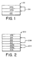
- the support layer 102 is an electrically insulating and optically transparent material such as glass or plastic.
- a bilayer 104 over the support layer 102 is formed of a conductive and transmissive layer 104a and a fluorocarbon overcoating layer 104b.
- the bilayer can be used as an anode for efficient hole injection in organic EL devices formed by polymer or small-molecule organic materials, as exemplified in FIG. 2.
- an organic electroluminescent device 200 is illustrative which uses a multilayer electrode in accordance with the present invention.
- An insulating and transparent support is layer 202.
- An anode 204 is formed of a conductive and transmissive layer 204a and a fluorocarbon overcoating layer 204b.
- the anode 204 is separated from a cathode 206 by an electroluminescent medium 208, which includes three superimposed layers.
- an organic hole transporting layer 210 Located on top of the anode layer 204 are, in sequence, an organic hole transporting layer 210, an organic luminescent layer 212, and an organic electron transporting layer 214.
- the electroluminescent medium can be a single layer or a bilayer comprising a hole transporting layer and an electron transporting layer. In such a configuration, the interface between the two layers provides an efficient site for the recombination of the injected hole-electron pair and resultant electroluminescence. It will also be understood that the electroluminescent medium can include more than three layers.
- the substrate 102 for electrode structure 100 shown in FIG. 1 and the substrate 202 for organic electroluminescent device 200 shown in FIG. 2 are electrically insulated and can either be light transmissive or opaque.
- the light transmissive property is desirable for viewing the EL emission through the substrate.
- the transmissive characteristic of the support is immaterial, and therefore any appropriate substrate such as opaque semiconductor and ceramic wafers can be used. Of course, it is necessary to provide in these device configurations a light transparent top electrode.
- the multilayer electrode 104 (see FIG. 1) and 204 (see FIG. 2), respectively, are formed of a conductive and transmissive layer 104a and 204a and a fluorocarbon overcoating layer 104b and 204b.
- the light transparent property of the layer 104a and 204a is desirable for viewing the EL emission through the substrate.
- the transmissive characteristic of the layer 104a and 204a is immaterial, and therefore any appropriate materials such as an opaque metal or metal compound having a work func ion greater than 4.1 eV can be used.
- the metals include gold, iridium, palladium, and platinum.
- the conductive and transmissive layer can be selected from the group of metal oxides, nitrides such as gallium nitride, selenides such as zinc selenide, and sulphides such as zinc sulphide.
- the suitable metal oxides include indium-tin oxide, aluminum- or indium-doped zinc oxide, tin oxide, magnesium-indium oxide, nickel-tungsten oxide, and cadmium-tin oxide.
- a layer mainly made of fluorocarbon 104b and 204b is formed on the conductive layer 104a and 204a, respectively.
- This fluorocarbon layer is an essential part in this invention. It has excellent durability for alkali or acid. It has a high work function, resulting in efficient hole injection and transport. It adheres well to the conductive layer and forms a buffer layer between the conductive layer and the hole transporting layer, thus significantly improving device operational stability.
- the surface of the aforementioned conductive layer my be processed beforehand to improve its adhesion to the fluorocarbon overcoating layer.
- the types of processing include sputtering processing, corona processing, UV irradiation, or oxygen plasma treatment.
- the thickness of the fluorocarbon is so selected that it would have a full coverage on the underlying conductive layer, and that its series resistance would not significantly affect device performance.
- a useful range of the thickness is from 1 to 200 nm, preferably 5-60 nm.
- This fluorocarbon layer can be deposited by many conventional means, s ich as spin-coating or dip-coating of Cyclized Perfluoro Polymer (CPFP), evaporation, and plasma polymerization using various gases containing carbon and fluorine such as decafluorobutane (C 4 F 10 ) and tetrafluoroethylene (CHF 3 ).
- composition of the EL medium is described as follows, with reference to device structure 200.
- the hole transporting layer of the organic EL device contains at least one hole transporting aromatic tertiary amine, where the latter is understood to be a compound containing at least one trivalent nitrogen atom that is bonded only to carbon atoms, at least one of which is a member of an aromatic ring.
- the aromatic tertiary amine can be an arylamine, such as a monarylamine, diarylamine, triarylamine, or a polymeric arylamine. Exemplary monomeric triarylamines are illustrated in US-A-3,180,730. Other suitable triarylamines substituted with vinyl or vinyl radicals and/or containing at least one active hydrogen containing group are disclosed in US-A-3,567,450 and US-A-3,658,520.
- the luminescent layer of the organic EL device comprises of a luminescent or fluorescent material where electroluminescence is produced as a result of electron-hole pair recombination in this region.
- the luminescent layer comprises of a single component, that is a pure material with a high fluorescent efficiency.
- a well known material is tris (8-quinolinato) aluminum, (Alq), which produces excellent green electroluminescence.
- a preferred embodiment of the luminescent layer comprises a multi-component material consisting of a host material doped with one or more components of fluorescent dyes. Using this method, highly efficient EL devices can be constructed. Simultaneously, the color of the EL devices can be tuned by using fluorescent dyes of different emission wavelengths in a common host material. This dopant scheme has been described in considerable details for EL devices using Alq as the host material in US-A-4,769,292.
- Preferred materials for use in forming the electron transporting layer of the organic EL devices of this invention are metal chelated oxinoid compounds, including chelates of oxine itself (also commonly referred to as 8-quinolinol or 8-hydroxyquinoline). Such compounds exhibit both high levels of performance and are readily fabricated in the form of thin layers.
- the organic EL devices of this invention can employ a cathode constructed of any metal having a work function lower than 4.0 eV, such as calcium and lithium.
- a cathode constructed of any metal having a work function lower than 4.0 eV, such as calcium and lithium.
- Unexpected fabrication, performance, and stability advantages have been realized by forming the cathode of a combination of a low work function metal and at least one other metal.
- U.S. Patent 4,885,211 by Tang and Van Slyke the disclosure of which is incorporated by reference herein.
- a bilayer structure of LiF/Al has been used to enhance electron injection, as disclosed in US-A-5,624,604.
- Fluorocarbon coating was carried out in a parallel plate RF reactor with CHF 3 at 500 mTorr and 100 W of power.
- a fluorocarbon layer with a thickness of about 20 nm was deposited on an indium-tin oxide coated glass substrate and analyzed with x- ray photoelectron spectroscopy (XPS). The peaks of CH, CF, CF 2 , and CF 3 were observed for the polymerized fluorocarbon layer.
- the ionization potential of the fluorocarbon layer was determined by ultraviolet photoelectron spectroscopy (UPS) to be greater than 9.0 eV.
- UPS ultraviolet photoelectron spectroscopy
- Contact angle measurement was performed t y observing the wettability of a water droplet on the layer surface. The layer was highly hydrophobic with a contact angle greater than 95°.
- the EL medium has three organic laye rs, namely, a CuPc layer, a hole transporting layer, and an electron transporting layer.
- the above sequence completed the deposition of the EL device.
- the device was then hermetically packaged in a dry glove box for protection against ambient environment.
- the drive voltage was 12 V at a current density of 100 mA/cm 2 .
- the luminescence output from this EL device was 0.45 mW/cm 2 when it was operated at 9 V.
- the device was then operated at 40 mA/cm 2 constant current with a 50% duty cycle, and both forward drive voltage and luminescence were measured. It was found that the drive voltage increased by one volt after operation for 2,000 hours. The luminescence progressively decreased and reached one half of its initial value after 2,000 hours.
- the EL medium has two organic layers, namely, a hole transporting layer and an electron transporting layer.
- the above sequence completed the deposition of the EL device.
- the device was then hermetically packaged in a dry glove box for protection against ambient environment.
- the drive voltage was 12.3 V at a current density of 100 mA/cm 2 .
- the luminescence output from this EL device was 0.40 mW/cm 2 when it was operated at 9 V. Stability tests at 40 mA/cm 2 constant current with a 50% duty cycle showed a rapid increase of applied voltages, indicating poor operational stability.
- the EL medium has two organic layers namely, a hole transporting layer and an electron transporting layer.
- the above sequence completed the deposition of the EL device.
- the device was then hermetically packaged in a dry glove box for protection against ambient environment.
- the drive voltage was 11 V at a current density of 100 mA/cm 2 .
- the luminescence output from this EL device was 1.36 mW/cm 2 when it was operated at 9 V.
- the operational stability of the device was found to be comparable with that disclosed in Example 1.
- the medium has two organic layers, namely, a hole transporting layer and an electron transporting layer.
- the above sequence completed the deposition of the EL device.
- the device was then hermetically packaged in a dry glove box for protection against ambient environment.
- the drive volta ge was 8.0 V at a current density of 100 mA/cm 2 .
- the luminescence output from this EL device was 4.5 mW/cm 2 when it was operated at 9 V.
- the device is extremely stable with a luminescence loss of less than 3% of its initial value after operation for 350 hours.
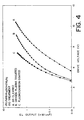
- FIG. 3. shows current density vs. drive voltage characteristics of the devices described in Examples 2, 3, and 4.
- FIG. 4 shows luminescence output of the three devices as a function of applied voltage.
- the results clearly indicate that an inventive device with a fluorocarbon-coated ITO anode can be operated at lower voltages and exhibits higher EL output at a fixed voltage, as compared to the prior art devices disclosed in Examples 1-3. This result was unexpected.
- FIG. 5 shows plots of operational stab ility for the devices shown in Examples 3 (prior art) and 4 (present invention). The drive voltage was found to remain constant in the both cases.
- the electroluminescence output from the device with an oxygen plasma-treated ITO anode decreased to approximately 75% of its initial value, while the loss of luminescence in the device with a fluorocarbon-coated ITO anode was about 3%.
- the medium has two organic layers, namely, a hole transporting layer and ar electron transporting layer.
- the above sequence completed the deposition of the EL device.
- the device was then hermetically packaged in a dry glove box for protection against ambient environment.
- the device wherein the organic medium includes an organic luminescent layer.
- the device wherein the organic medium includes an organic hole transporting layer and an organic electron transporting layer.
- the device wherein the organic medium includes an organic hole transporting layer, an organic luminescent layer, and an organic electron transporting layer.
- the device wherein the organic medium includes polymer materials and small-molecule organic materials.
Landscapes
- Physics & Mathematics (AREA)
- Optics & Photonics (AREA)
- Electroluminescent Light Sources (AREA)
- Laminated Bodies (AREA)
- Non-Insulated Conductors (AREA)
Applications Claiming Priority (2)
| Application Number | Priority Date | Filing Date | Title |
|---|---|---|---|
| US96143397A | 1997-10-30 | 1997-10-30 | |
| US961433 | 1997-10-30 |
Publications (2)
| Publication Number | Publication Date |
|---|---|
| EP0914025A1 EP0914025A1 (en) | 1999-05-06 |
| EP0914025B1 true EP0914025B1 (en) | 2002-04-10 |
Family
ID=25504464
Family Applications (1)
| Application Number | Title | Priority Date | Filing Date |
|---|---|---|---|
| EP98203511A Expired - Lifetime EP0914025B1 (en) | 1997-10-30 | 1998-10-19 | A multistructured electrode for use with electroluminescent devices |
Country Status (3)
| Country | Link |
|---|---|
| EP (1) | EP0914025B1 (enExample) |
| JP (1) | JP4372871B2 (enExample) |
| DE (1) | DE69804747T2 (enExample) |
Families Citing this family (11)
| Publication number | Priority date | Publication date | Assignee | Title |
|---|---|---|---|---|
| US6208075B1 (en) * | 1998-11-05 | 2001-03-27 | Eastman Kodak Company | Conductive fluorocarbon polymer and method of making same |
| US6208077B1 (en) * | 1998-11-05 | 2001-03-27 | Eastman Kodak Company | Organic electroluminescent device with a non-conductive fluorocarbon polymer layer |
| JP3591387B2 (ja) * | 1999-09-22 | 2004-11-17 | 富士電機ホールディングス株式会社 | 有機el素子 |
| CN100531500C (zh) * | 2001-12-21 | 2009-08-19 | 国际商业机器公司 | 电子器件和光电器件的电极结构 |
| WO2004068912A1 (ja) | 2003-01-30 | 2004-08-12 | Fujitsu Limited | 正孔注入層用材料、有機el素子及び有機elディスプレイ |
| JP5165193B2 (ja) * | 2004-08-27 | 2013-03-21 | 昭和電工株式会社 | 有機発光素子及びその製造方法 |
| CN100570919C (zh) * | 2004-08-27 | 2009-12-16 | 昭和电工株式会社 | 有机电致发光器件及其制造方法 |
| KR101156014B1 (ko) | 2004-08-27 | 2012-06-18 | 쇼와 덴코 가부시키가이샤 | 유기전계발광소자의 제조방법 |
| DE102007024152A1 (de) | 2007-04-18 | 2008-10-23 | Osram Opto Semiconductors Gmbh | Organisches optoelektronisches Bauelement |
| TWI481308B (zh) | 2007-09-27 | 2015-04-11 | Semiconductor Energy Lab | 發光元件,發光裝置,與電子設備 |
| CN103824969B (zh) * | 2014-03-10 | 2016-03-23 | 太原理工大学 | 具有多层金属复合电极的有机电致发光器件 |
Family Cites Families (2)
| Publication number | Priority date | Publication date | Assignee | Title |
|---|---|---|---|---|
| US5491377A (en) * | 1993-08-03 | 1996-02-13 | Janusauskas; Albert | Electroluminescent lamp and method |
| JPH09180882A (ja) * | 1995-12-27 | 1997-07-11 | Nec Kansai Ltd | 電界発光灯 |
-
1998
- 1998-10-19 DE DE69804747T patent/DE69804747T2/de not_active Expired - Lifetime
- 1998-10-19 EP EP98203511A patent/EP0914025B1/en not_active Expired - Lifetime
- 1998-10-29 JP JP30884298A patent/JP4372871B2/ja not_active Expired - Lifetime
Also Published As
| Publication number | Publication date |
|---|---|
| JPH11219790A (ja) | 1999-08-10 |
| JP4372871B2 (ja) | 2009-11-25 |
| EP0914025A1 (en) | 1999-05-06 |
| DE69804747T2 (de) | 2002-11-21 |
| DE69804747D1 (de) | 2002-05-16 |
Similar Documents
| Publication | Publication Date | Title |
|---|---|---|
| US6208077B1 (en) | Organic electroluminescent device with a non-conductive fluorocarbon polymer layer | |
| US6069442A (en) | Organic electroluminescent device with inorganic electron transporting layer | |
| US6351067B2 (en) | Organic electroluminescent device with improved hole injecting structure | |
| US6483236B1 (en) | Low-voltage organic light-emitting device | |
| JP5583345B2 (ja) | 有機層の層構造を備える電子デバイス | |
| EP0977286B1 (en) | Organic light emitting device | |
| EP1010359B1 (en) | Color variable bipolar/ac light-emitting devices | |
| EP0977287A2 (en) | Interfacial electron-injecting layer formed from a doped cathode for organic light-emitting structure | |
| EP1076368A2 (en) | A surface-emitting organic light-emitting diode | |
| JP4789209B2 (ja) | 正孔輸送領域内の金属副層 | |
| EP0977288A2 (en) | Electron-injecting layer formed from a dopant layer for organic light-emitting structure | |
| JP2007507107A (ja) | 非正孔阻止バッファ層を有するoled | |
| US7449832B2 (en) | Organic electroluminescence device and organic electroluminescence display | |
| KR20030027819A (ko) | 정공 수송층과 발광층 사이에 계면층을 갖는 유기 발광다이오드 | |
| US6995391B2 (en) | Electrode structure for electronic and opto-electronic devices | |
| JP2004127937A (ja) | 有機電場発光デバイス及びその製造方法 | |
| EP0914025B1 (en) | A multistructured electrode for use with electroluminescent devices | |
| US6917158B2 (en) | High-qualty aluminum-doped zinc oxide layer as transparent conductive electrode for organic light-emitting devices | |
| JPH11219790A5 (enExample) | ||
| US8102114B2 (en) | Method of manufacturing an inverted bottom-emitting OLED device | |
| KR100790672B1 (ko) | 유기 일렉트로루미네센스 소자 및 유기 일렉트로루미네센스디스플레이 | |
| US7402947B2 (en) | Anode for organic light emitting diode | |
| US20020182307A1 (en) | Organic electroluminescent devices with organic layers deposited at elevated substrate temperatures | |
| KR100280961B1 (ko) | 안정성이향상된저전압구동유기발광소자 | |
| Riel et al. | Influence of charge carrier injection on the device performance of blue organic light-emitting diodes |
Legal Events
| Date | Code | Title | Description |
|---|---|---|---|
| PUAI | Public reference made under article 153(3) epc to a published international application that has entered the european phase |
Free format text: ORIGINAL CODE: 0009012 |
|
| AK | Designated contracting states |
Kind code of ref document: A1 Designated state(s): DE FR GB |
|
| AX | Request for extension of the european patent |
Free format text: AL;LT;LV;MK;RO;SI |
|
| 17P | Request for examination filed |
Effective date: 19991016 |
|
| AKX | Designation fees paid |
Free format text: DE FR GB |
|
| 17Q | First examination report despatched |
Effective date: 20010124 |
|
| GRAG | Despatch of communication of intention to grant |
Free format text: ORIGINAL CODE: EPIDOS AGRA |
|
| GRAG | Despatch of communication of intention to grant |
Free format text: ORIGINAL CODE: EPIDOS AGRA |
|
| GRAH | Despatch of communication of intention to grant a patent |
Free format text: ORIGINAL CODE: EPIDOS IGRA |
|
| REG | Reference to a national code |
Ref country code: GB Ref legal event code: IF02 |
|
| GRAH | Despatch of communication of intention to grant a patent |
Free format text: ORIGINAL CODE: EPIDOS IGRA |
|
| GRAA | (expected) grant |
Free format text: ORIGINAL CODE: 0009210 |
|
| AK | Designated contracting states |
Kind code of ref document: B1 Designated state(s): DE FR GB |
|
| REF | Corresponds to: |
Ref document number: 69804747 Country of ref document: DE Date of ref document: 20020516 |
|
| ET | Fr: translation filed | ||
| PLBE | No opposition filed within time limit |
Free format text: ORIGINAL CODE: 0009261 |
|
| STAA | Information on the status of an ep patent application or granted ep patent |
Free format text: STATUS: NO OPPOSITION FILED WITHIN TIME LIMIT |
|
| 26N | No opposition filed |
Effective date: 20030113 |
|
| REG | Reference to a national code |
Ref country code: FR Ref legal event code: TP |
|
| REG | Reference to a national code |
Ref country code: GB Ref legal event code: 732E Free format text: REGISTERED BETWEEN 20110224 AND 20110302 |
|
| REG | Reference to a national code |
Ref country code: FR Ref legal event code: PLFP Year of fee payment: 19 |
|
| REG | Reference to a national code |
Ref country code: FR Ref legal event code: PLFP Year of fee payment: 20 |
|
| PGFP | Annual fee paid to national office [announced via postgrant information from national office to epo] |
Ref country code: FR Payment date: 20170918 Year of fee payment: 20 |
|
| PGFP | Annual fee paid to national office [announced via postgrant information from national office to epo] |
Ref country code: DE Payment date: 20171011 Year of fee payment: 20 |
|
| PGFP | Annual fee paid to national office [announced via postgrant information from national office to epo] |
Ref country code: GB Payment date: 20171018 Year of fee payment: 20 |
|
| REG | Reference to a national code |
Ref country code: DE Ref legal event code: R071 Ref document number: 69804747 Country of ref document: DE |
|
| REG | Reference to a national code |
Ref country code: GB Ref legal event code: PE20 Expiry date: 20181018 |
|
| PG25 | Lapsed in a contracting state [announced via postgrant information from national office to epo] |
Ref country code: GB Free format text: LAPSE BECAUSE OF EXPIRATION OF PROTECTION Effective date: 20181018 |