EP0913836B1 - Schaltungsanordnung zur Erzeugung einer Spannung zum Programmieren oder Löschen von Halbleiter-Speicherzellen mit schwebendem Gate - Google Patents
Schaltungsanordnung zur Erzeugung einer Spannung zum Programmieren oder Löschen von Halbleiter-Speicherzellen mit schwebendem Gate Download PDFInfo
- Publication number
- EP0913836B1 EP0913836B1 EP98470024A EP98470024A EP0913836B1 EP 0913836 B1 EP0913836 B1 EP 0913836B1 EP 98470024 A EP98470024 A EP 98470024A EP 98470024 A EP98470024 A EP 98470024A EP 0913836 B1 EP0913836 B1 EP 0913836B1
- Authority
- EP
- European Patent Office
- Prior art keywords
- voltage
- programming
- circuit
- pumped
- control signal
- Prior art date
- Legal status (The legal status is an assumption and is not a legal conclusion. Google has not performed a legal analysis and makes no representation as to the accuracy of the status listed.)
- Expired - Lifetime
Links
- 230000015654 memory Effects 0.000 title claims description 21
- 238000007493 shaping process Methods 0.000 claims description 21
- 238000005086 pumping Methods 0.000 claims description 10
- 238000001514 detection method Methods 0.000 claims description 8
- 238000000034 method Methods 0.000 claims description 7
- 230000007935 neutral effect Effects 0.000 claims description 4
- 230000000750 progressive effect Effects 0.000 claims description 4
- 230000000694 effects Effects 0.000 description 7
- 230000033228 biological regulation Effects 0.000 description 5
- 238000010586 diagram Methods 0.000 description 3
- 230000006870 function Effects 0.000 description 3
- 230000001105 regulatory effect Effects 0.000 description 3
- 230000000630 rising effect Effects 0.000 description 3
- 230000007423 decrease Effects 0.000 description 2
- 238000009877 rendering Methods 0.000 description 2
- 239000003990 capacitor Substances 0.000 description 1
- 230000015556 catabolic process Effects 0.000 description 1
- 238000012217 deletion Methods 0.000 description 1
- 230000037430 deletion Effects 0.000 description 1
- 238000009413 insulation Methods 0.000 description 1
- 238000004519 manufacturing process Methods 0.000 description 1
- 244000045947 parasite Species 0.000 description 1
- 230000010287 polarization Effects 0.000 description 1
- 230000005855 radiation Effects 0.000 description 1
- 239000007858 starting material Substances 0.000 description 1
Images


Classifications
-
- G—PHYSICS
- G11—INFORMATION STORAGE
- G11C—STATIC STORES
- G11C16/00—Erasable programmable read-only memories
- G11C16/02—Erasable programmable read-only memories electrically programmable
- G11C16/06—Auxiliary circuits, e.g. for writing into memory
- G11C16/30—Power supply circuits
-
- G—PHYSICS
- G11—INFORMATION STORAGE
- G11C—STATIC STORES
- G11C16/00—Erasable programmable read-only memories
- G11C16/02—Erasable programmable read-only memories electrically programmable
- G11C16/06—Auxiliary circuits, e.g. for writing into memory
- G11C16/10—Programming or data input circuits
- G11C16/12—Programming voltage switching circuits
-
- G—PHYSICS
- G11—INFORMATION STORAGE
- G11C—STATIC STORES
- G11C5/00—Details of stores covered by group G11C11/00
- G11C5/14—Power supply arrangements, e.g. power down, chip selection or deselection, layout of wirings or power grids, or multiple supply levels
- G11C5/145—Applications of charge pumps; Boosted voltage circuits; Clamp circuits therefor
Definitions
- the invention relates to a circuit for generating voltage to program or erase a memory which uses floating gate transistors.
- the invention relates more particularly to the generator which provides memory cells with slots for voltage in order to erase or program them.
- Programming and erasing information contained in floating gate transistors is by applying high voltages between grid and drain to load or unload the floating grid by tunnel effect.
- the voltage to apply to the transistor must be progressive in order to avoid a breakdown of the insulation.
- Many voltage ramp generators are known. A ramp generator system is described for example in applications EP-A-0 762 428 and EP-A-O 811 987.
- FIG. 1 there is shown the circuits implemented during the programming of a floating gate memory.
- a charge pump 1 supplies a so-called pumped voltage V HT .
- This charge pump 1 is controlled by a programming signal SP of the binary type.
- the programming signal SP authorizes the operation of the charge pump during programming.
- a shaping circuit 2 receives the pumped voltage V HT and produces a programming voltage Vpp whose growth is gradually regulated so as not to damage the storage transistors.
- the programming voltage Vpp is used to supply buffer registers 3 into which the data to be programmed has been previously loaded.
- One or more of the buffer registers 3 is connected to a memory plane 4.
- the increase in the programming voltage V PP causes the progressive increase in the voltage at the output of the buffer registers 3 which has the effect of writing the content of at least one of the buffer registers 3 in the memory plane.
- deletion is carried out according to a similar principle with some differences, however.
- the ideal operation, for a voltage slot, of the charge pump 1 and of the shaping circuit 2 is shown in FIG. 2a.
- the programming signal is activated, which causes the rapid growth of the pumped voltage V HT which will increase to a maximum pumped voltage V HTMAX , the pumped voltage V HT being regulated to be maintained at V HTMAX .
- the programming signal is deactivated which ends the programming, the charge pump 1 stops and the pumped voltage V HT decreases to 0 V.
- the voltage V PP is a constant voltage equal to the supply voltage V CC of the integrated circuit when the programming signal SP is deactivated.
- the programming voltage Vpp becomes equal to the pumped voltage V HT .
- the shaping circuit limits the growth of the programming voltage Vpp so as not to damage the storage transistors.
- Figure 2a corresponds to normal operation with a charge pump which can supply sufficient current.
- the charge pump must supply a current to the circuits supplied by the programming voltage V PP , that is to say the buffer registers 3 loaded by the storage plane storage transistors to which they are connected. .
- the current supplied by the charge pump is all the more important as the growth of the programming voltage Vpp is significant.
- FIG. 2b represents an extreme case where the charge pump 1 does not make it possible to reach the voltage V HTMAX necessary for ensuring programming.
- a person skilled in the art must size the charge pump 1 according to the maximum current which it will have to supply while being able to rapidly increase the pumped voltage V HT .
- the maximum output current of the charge pump is proportional to C * F / n, C being the capacity of the capacitors used in the output stages of the pump, F being the pumping frequency, and n the number of pump output stages.
- the number of output stages is fixed according to the desired voltage and the supply voltage of the integrated circuit.
- the increase in the pumping frequency leads to an increase in consumption, problems with the emission of parasites (radiation), and the risks of stalling (switching of the output stages too fast).
- the increase in capacity leads to an increase in the size of the pump.
- the invention proposes to solve the problems of oversizing of the pump under load.
- a switching circuit is added to switch the pumped voltage after a certain time to the pumped voltage reaches a sufficient level before to have to draw a strong current.
- the charge pump according to the invention should be calculated only for maintain the pumped voltage at its maximum value in charge which allows to have a charge pump of smaller size.
- the subject of the invention is a grid memory floating according to claim 1 and a method according to claim 5.
- the means either have a detection circuit voltage to detect that the pumped voltage has reached a reference voltage and make the signal active control as soon as the pumped voltage has reached the voltage reference, i.e. a timing circuit for activate the control signal after a period predetermined has elapsed from the implementation charge pump route, or either a circuit of voltage detection and a timing circuit for activate the control signal as soon as the voltage pumped has reached a reference voltage or as soon as the charge pump has been activated for a period of time predetermined.
- the switching circuit provides equal switched voltage at the voltage pumped to the shaping circuit when the control signal is active.
- the control signal becomes active either as soon as the pumped voltage has reached a reference voltage, either as soon as a duration predetermined time has elapsed after the pumping of the pumped voltage, or either as soon as the pumped voltage has reaches a reference voltage or as soon as a duration predetermined time has elapsed after the pumping of the pumped voltage.
- the circuit shown includes the charge pump 1, the shaping circuit 2, a timer circuit 5, a logic circuit 6 and a switching circuit 7.
- the charge pump 1 has been detailed and comprises output stages connected in series, a circuit phase generator 102, an oscillator 103, and a regulation circuit 104.
- the output stages 101 each receive at least one or two phase signals (depending on the type of output stages), an input voltage and each supply an output voltage equal to the input voltage increased by the amplitude of the phase signal in steady state.
- the first of the output stages 101 receives the supply voltage of the circuit V CC and the last output stage 101 supplies the pumped voltage VHT.
- the phase generator 102 receives a signal clock and produces two or four phase signals to the output stages alternately.
- Oscillator 103 is of the controlled type and has first and second command inputs and provides on an output the clock signal.
- the oscillator works when the first and second entries are both in a first state and stops as soon as one of the inputs is in the second state.
- the first input of oscillator 103 receives the SP programming signal which indicates that the programming is in progress when it is in the first state.
- the regulation circuit 104 receives the pumped voltage V HT and produces a binary indicator IB on an output.
- the output of the regulation circuit 104 is connected to the second input of the oscillator 103.
- the binary indicator IB is in the first state.
- the binary indicator IB is in the second state.
- Timing circuit 5 having an input and an output, receives on its input the signal of programming and produces an end of FT time delay on its output.
- the end of indicator FT time delay is a binary type signal which positions in the first state after a duration predetermined has elapsed from a rising edge of the programming signal SP. When the signal from SP programming is in the second state, the signal end of delay is positioned in the second state.
- the timer circuit 5 can for example be realized using a monostable circuit or using a counter.
- Logic circuit 6 has first to third binary inputs and a logic output.
- the first binary input is connected to the output of the regulator circuit 104 for receiving the binary indicator IB.
- the second binary input receives the signal from SP programming.
- the third binary input receives the FT timeout indicator.
- the exit logic provides a control signal SC which is inactive when the programming signal is in the second state and which becomes active as soon as the signal SP programming is in the first state and that the binary indicator IB has a rising edge or from that the programming signal SP is in the first state and that the FT timeout signal is present a rising front.
- the switching circuit 7 has a control input, a voltage input and a voltage output.
- the voltage input receives the pumped voltage V HT .
- the control input receives the control signal SC.
- the voltage output provides a switched voltage V HT 'which is zero when the control signal is inactive and which is equal to the pumped voltage V HT when the control signal is active.
- the shaping circuit 2 receives the switched voltage V HT 'and supplies the programming voltage Vpp.
- the programming voltage Vpp is equal to the supply voltage V CC when the switched voltage V HT 'is zero. As soon as the switched voltage V HT 'is greater than the supply voltage V CC , the programming voltage Vpp will increase gradually until reaching a maximum value of programming voltage.
- the shaping circuit can for example be that described in application EP-A-0 762 428.
- the switching circuit 7 supplies a neutral voltage to the shaping circuit 2.
- neutral voltage By neutral voltage, one must understand a voltage which makes the shaping circuit inactive, for example, the neutral voltage can be between 0 V and the supply voltage V DC , or even correspond to a high impedance type output whose voltage is fixed by the shaping circuit 2.
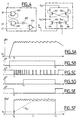
- FIG. 4 represents an embodiment preferred of logic circuit 6 and switching circuit 7.
- Logic circuit 6 includes first and second doors AND-NO 601 and 602 with two inputs, one inverting door 603, and an ON-OFF door 604 with two starters.
- the first and second doors ET-NON 601 and 602 are connected to form a / R / S type flip-flop, an entrance to the first door AND-NO 601 receiving the binary indicator IB, and an entry for the second AND-NO gate 602 receiving the programming signal SP.
- the input of the reversing door 603 is connected to the exit of the second door ET-NON 602.
- the first door input YES-NO 604 is connected to the output of the reversing door 603.
- the second entry of the door YES-NO 604 receives the end of delay signal FT.
- the output of the door NO-NO 604 provides the signal for SC command.
- the switching circuit 7 comprises first and second P-type transistors 701 and 702, third and fourth N-type transistors 703 and 704, and an inverter 705.
- the sources of the first and second transistors 701 and 702 are connected together and receive the pumped voltage V HT .
- the drain of the first transistor 701 is connected to the gate of the second transistor 702 and to the drain of the third transistor 703.
- the drain of the second transistor 702 is connected to the gate of the first transistor 701 and to the drain of the fourth transistor 704.
- the sources of the third and fourth transistors 703 and 704 are connected to ground.
- the gate of the third transistor 703 and the input of the inverter 705 are connected together to the output of the logic circuit 6 and receive the control signal SC.
- the gate of the fourth transistor 704 is connected to the output of the inverter 705.
- the switched voltage V HT ' is supplied by the node formed by the drains of the first and third transistors 701 and 703.
- the invention can be summarized as a delay in the supply of the pumped voltage V HT to the shaping circuit 2.
- the delay is induced in the preferred example by a control circuit which comprises a voltage detection circuit which is the control circuit 104 of the charge pump 1, the timing circuit 5 and the logic circuit 6.
- FIGS. 5A to 5F represent the operating timing diagrams of the invention in the case where the charge pump is "fast".
- V DC supply voltage
- V RE reference voltage
- V TC maximum programming voltage
- FIG. 5A represents the pumped voltage V HT of the charge pump output.
- the saw teeth correspond to the pumping of the charge pump and are relatively accentuated compared to reality.
- FIGS. 5B to 5D respectively represent the programming signal SP, the binary indicator IB and the FT timeout signal.
- the first state corresponds to a logic state "1" and the second state corresponds to a logical state "0".
- FIG. 5E represents the control signal SC, here active at logic level "0".
- FIG. 5F represents the switched voltage V HT 'in solid line and the programming voltage Vpp in dotted line.
- the programming voltage V PP presents a simple growth in order to simplify the drawing.
- the programming signal becomes active, which triggers the pumping of the charge pump 1.
- the pumped voltage reaches the maximum value which positions the binary indicator IB in the second state, the control signal becomes active, making the switched voltage V HT 'equal to the pumped voltage V HT and therefore the programming voltage Vpp will increase.
- the time-out ends, the end-of-time-out signal goes into the first state without affecting the rest of the circuit.
- the programming voltage V PP reaches its maximum value.
- the programming signal SP goes into the second state, indicating the end of the programming, which has the effect of rendering the control signal SC inactive and making the switched voltage V HT 'zero, the programming voltage V PP then becomes equal to the supply voltage V CC .
- FIGS. 6A to 6F represent the operating timing diagrams of the invention in the case where the charge pump is "slow".
- V DC supply voltage
- V RE reference voltage
- FIG. 6A represents the pumped voltage V HT of the charge pump output.
- the saw teeth correspond to the pumping of the charge pump and are relatively accentuated compared to reality.
- FIGS. 6B to 6D respectively represent the programming signal SP, the binary indicator IB and the FT timeout signal.
- the first state corresponds to a logic state "1" and the second state corresponds to a logical state "0".
- FIG. 6E represents the control signal SC, here active at logic level "0".
- FIG. 6F represents the switched voltage V HT 'in solid line and the programming voltage Vpp in dotted line.
- the programming voltage Vpp presents a simple growth in order to simplify the drawing.
- the programming signal becomes active, which triggers the pumping of the charge pump 1.
- the timeout ends, the end of timeout signal goes into the first state, the control signal becomes active, making the switched voltage V HT 'equal to the pumped voltage V HT and therefore the programming voltage Vpp will increase.
- the pumped voltage reaches the maximum value which positions the binary indicator IB in the second state, without affecting the rest of the circuit.
- the programming voltage Vpp reaches its maximum value.
- the programming signal SP goes into the second state, indicating the end of the programming, which has the effect of rendering the control signal SC inactive and making the switched voltage V HT 'zero, the programming voltage V PP then becomes equal to the supply voltage V CC .
- the increase in the programming voltage calls for a greater current than between instants t 9 and t 10 , which results in greater demand on the charge pump, which influences the value of the pumped voltage VHT.
- the pumped voltage V HT has not yet reached the reference voltage, the growth of the pumped voltage is slowed down.
- the time delay allowed the pumped voltage V HT to reach a sufficient level for a sufficient duration, which makes it possible to have correct operation of the shaping circuit 2.
- control circuit uses the combination of two conditions, one on the pumped voltage and the other time, via of an OR function. It is possible to be satisfied with a control circuit using a single condition and using either a voltage detection circuit or a timing circuit.
- the predetermined time must be calculated so that after this time , it is certain that the pumped voltage V HT has reached a sufficient level.
- the tolerances on the actual values of the capacities and resistances of an integrated circuit tend to calculate the predetermined duration as a function of the worst case that may arise when the pumped voltage V HT rises .
- the duration thus calculated is relatively high for all circuits which function better than the worst case (ie 99% of the circuits produced).
- the use of the predetermined duration alone has the effect of making the duration of application of the maximum programming voltage fixed by reproducing the worst case, which has the effect of increasing the programming time.
Landscapes
- Engineering & Computer Science (AREA)
- Power Engineering (AREA)
- Read Only Memory (AREA)
- Dc-Dc Converters (AREA)
- Dram (AREA)
Claims (8)
- Speicher mit schwimmendem Gate, mit einer Schaltung zum Erzeugen einer Spannung zum Programmieren oder Löschen, wobei die Schaltung zum Erzeugen einer hohen Spannung eine Ladungspumpe (1) zum Liefern einer so genannten Pumpspannung (VHT) und einen Pulsformer (2) zum Liefern einer so genannten Programmier- oder Löschspannung (VPP) ausgehend von der Pumpspannung (VHT) aufweist, wobei der Anstieg der Programmier-oder Löschspannung (VPP) progressiv ist,
dadurch gekennzeichnet, dass die Schaltung Steuerungsmittel (5, 6, 104) zum Liefern eines Steuersignals (SC) und einen zwischen der Ladungspumpe und dem Pulsformer angeschlossenen Umschalter (7) aufweist, wobei der Umschalter eine Schaltspannung (VHT') an den Pulsformer (2) liefert, die abhängig vom Steuersignal (SC) entweder gleich der Pumpspannung (VHT) oder gleich einer neutralen Spannung (0V) ist, wobei das Steuersignal (SC) aktiv ist, wenn die Pumpspannung ein ausreichendes Spannungsniveau erreicht hat. - Speicher nach Anspruch 1, dadurch gekennzeichnet, dass die Steuermittel eine Spannungsdetektorschaltung (104) aufweisen, um zu ermitteln, ob die Pumpspannung (VHT) eine Referenzspannung erreicht hat, und das Steuersignal (SC) aktiv zu setzen, sobald die Pumpspannung (VHT) die Referenzspannung erreicht hat, und dadurch, dass der Umschalter (7) die der Pumpspannung (VHT) gleiche Schaltspannung (VHT') an den Pulsformer (2) liefert, wenn das Steuersignal (SC) aktiv ist.
- Speicher nach Anspruch 1, dadurch gekennzeichnet, dass die Steuermittel einen Verzögerungskreis (5) aufweisen, um das Steuersignal (SC) aktiv zu setzen, nachdem eine vorher festgelegte Zeitspanne ab Ingangsetzen der Ladungspumpe (1) verstrichen ist, und dadurch, dass der Umschalter (7) die der Pumpspannung (VHT') gleiche Schaltspannung (VHT') an den Pulsformer (2) liefert, wenn das Steuersignal (SC) aktiv ist.
- Speicher nach Anspruch 1, dadurch gekennzeichnet, dass die Steuermittel eine Spannungsdetektorschaltung (104) und einen Verzögerungskreis (5) aufweisen, um das Steuersignal (SC) aktiv zu setzen, sobald die Pumpspannung (VHT) eine Referenzspannung erreicht hat oder sobald die Ladungspumpe (1) eine vorher festgelegte Zeitspanne lang aktiviert ist, und dadurch dass der Umschalter (7) die der Pumpspannung (VHT) gleiche Schaltspannung (VHT') an den Pulsformer (2) liefert, wenn das Steuersignal (SC) aktiv ist.
- Verfahren zum Erzeugen einer Programmier- oder Löschspannung für einen Speicher mit schwimmendem Gate, bei dem eine Pumpspannung (VHT) von einer Ladungspumpe (1) erzeugt wird und eine Programmier- oder Löschspannung (VPP) ausgehend von der Pumpspannung (VHT) in einem Pulsformer (2) erzeugt wird, wobei die Programmier- oder Löschspannung (VPP) progressiv ansteigt,
dadurch gekennzeichnet, dass die Pumpspannung (VHT) an den Pulsformer (2) geliefert wird, wenn ein aktives Steuersignal (SC) erhalten wird, wobei das Steuersignal (SC) aktiv ist, wenn die Pumpspannung (VHT) ein ausreichendes Spannungsniveau erreicht hat. - Verfahren nach Anspruch 5, dadurch gekennzeichnet, dass das Steuersignal (SC) aktiv wird, sobald die Pumpspannung (VHT) die Referenzspannung erreicht hat.
- Verfahren nach Anspruch 5, dadurch gekennzeichnet, dass das Steuersignal (SC) aktiv wird, nachdem eine vorher festgelegte Zeitspanne nach Beginn des Pumpens der Pumpspannung (VHT) verstrichen ist.
- Verfahren nach Anspruch 5, dadurch gekennzeichnet, dass das Steuersignal (SC) aktiv wird, sobald die Pumpspannung (VHT) eine Referenzspannung erreicht hat oder sobald eine vorher festgelegte Zeitspanne nach Beginn des Pumpens der Pumpspannung (VHT) verstrichen ist.
Applications Claiming Priority (2)
| Application Number | Priority Date | Filing Date | Title |
|---|---|---|---|
| FR9713751 | 1997-10-29 | ||
| FR9713751A FR2770325B1 (fr) | 1997-10-29 | 1997-10-29 | Circuit generateur de tension pour programmer ou effacer une memoire qui utilise des transistors a grille flottante |
Publications (2)
| Publication Number | Publication Date |
|---|---|
| EP0913836A1 EP0913836A1 (de) | 1999-05-06 |
| EP0913836B1 true EP0913836B1 (de) | 2001-07-18 |
Family
ID=9512933
Family Applications (1)
| Application Number | Title | Priority Date | Filing Date |
|---|---|---|---|
| EP98470024A Expired - Lifetime EP0913836B1 (de) | 1997-10-29 | 1998-10-12 | Schaltungsanordnung zur Erzeugung einer Spannung zum Programmieren oder Löschen von Halbleiter-Speicherzellen mit schwebendem Gate |
Country Status (4)
| Country | Link |
|---|---|
| US (1) | US5978268A (de) |
| EP (1) | EP0913836B1 (de) |
| DE (1) | DE69801143T2 (de) |
| FR (1) | FR2770325B1 (de) |
Families Citing this family (5)
| Publication number | Priority date | Publication date | Assignee | Title |
|---|---|---|---|---|
| FR2782421B1 (fr) * | 1998-08-11 | 2000-09-15 | St Microelectronics Sa | Dispositif de generation d'une haute tension |
| FR2821974B1 (fr) * | 2001-03-12 | 2003-05-23 | St Microelectronics Sa | Circuit et procede associe d'effacement ou de programmation d'une cellule memoire |
| US6965263B2 (en) * | 2002-10-10 | 2005-11-15 | Micron Technology, Inc. | Bulk node biasing method and apparatus |
| JP2008112507A (ja) * | 2006-10-30 | 2008-05-15 | Toshiba Corp | 半導体記憶装置 |
| US8116140B2 (en) | 2010-04-09 | 2012-02-14 | Sandisk Technologies Inc. | Saw-shaped multi-pulse programming for program noise reduction in memory |
Family Cites Families (7)
| Publication number | Priority date | Publication date | Assignee | Title |
|---|---|---|---|---|
| US5101381A (en) * | 1987-08-31 | 1992-03-31 | Oki Electric Industry Co., Ltd. | Control circuit for EEPROM |
| GB2288678B (en) * | 1991-11-07 | 1996-04-03 | Samsung Electronics Co Ltd | Voltage pumping circuits |
| KR960000837B1 (ko) * | 1992-12-02 | 1996-01-13 | 삼성전자주식회사 | 반도체 메모리장치 |
| US5408133A (en) * | 1993-05-03 | 1995-04-18 | Delco Electronics Corporation | Ramp control circuit |
| JPH0721790A (ja) * | 1993-07-05 | 1995-01-24 | Mitsubishi Electric Corp | 半導体集積回路 |
| FR2748616B1 (fr) * | 1996-05-07 | 1998-06-12 | Sgs Thomson Microelectronics | Circuit de production d'une haute tension de programmation |
| FR2749698B1 (fr) * | 1996-06-07 | 1998-09-04 | Inside Technologies | Memoire remanente effacable et programmable electriquement, protegee contre les coupures d'alimentation |
-
1997
- 1997-10-29 FR FR9713751A patent/FR2770325B1/fr not_active Expired - Fee Related
-
1998
- 1998-10-12 DE DE69801143T patent/DE69801143T2/de not_active Expired - Fee Related
- 1998-10-12 EP EP98470024A patent/EP0913836B1/de not_active Expired - Lifetime
- 1998-10-27 US US09/179,635 patent/US5978268A/en not_active Expired - Lifetime
Also Published As
| Publication number | Publication date |
|---|---|
| DE69801143D1 (de) | 2001-08-23 |
| FR2770325B1 (fr) | 2001-10-05 |
| US5978268A (en) | 1999-11-02 |
| DE69801143T2 (de) | 2001-11-08 |
| FR2770325A1 (fr) | 1999-04-30 |
| EP0913836A1 (de) | 1999-05-06 |
Similar Documents
| Publication | Publication Date | Title |
|---|---|---|
| EP0313431B1 (de) | Verfahren zur Programmierung von Speicherzellen und Schaltkreis für die Durchführung dieses Verfahrens | |
| FR2689294A1 (fr) | Circuit de pompage de tension à utiliser dans des dispositifs de mémoire à semi-conducteur. | |
| FR2761214A1 (fr) | Circuit elevateur de tension du type pompe de charge a nombre d'etages controle | |
| FR2466834A1 (fr) | Procede de programmation pour une memoire non volatile a semi-conducteur modifiable electriquement | |
| FR2778012A1 (fr) | Dispositif et procede de lecture de cellules de memoire eeprom | |
| FR2627315A1 (fr) | Procede de preconditionnement, effacement et/ou programmation d'un composant de memoire eeprom | |
| EP1094604B1 (de) | Spannungserhöhungsschaltung des Ladungspumpen-Typs | |
| FR2665973A1 (fr) | Circuit d'optimisation d'effacement automatique pour une memoire a semiconducteur programmable et effacable electriquement et procede s'y rapportant. | |
| FR2749698A1 (fr) | Memoire remanente effacable et programmable electriquement, protegee contre les coupures d'alimentation | |
| EP0750244B1 (de) | Ladungspumpe-Generator-Schaltkreis für negative Spannung | |
| EP0913836A1 (de) | Schaltungsanordnung zur Erzeugung einer Spannung zum Programmieren oder Löschen von Halbleiter-Speicherzellen mit schwebendem Gate | |
| CA2262995C (fr) | Circuit integre a fonctionnement sans contact, comportant une pompe de charges | |
| EP3147909B1 (de) | Verfahren zur kontrolle eines schreibzyklus eines speichers vom typ eeprom, und entsprechende vorrichtung | |
| FR2801419A1 (fr) | Procede et dispositif de lecture pour memoire en circuit integre | |
| EP0703584B1 (de) | Adressen-Dekodierverfahren für einen integrierten Speicher und Speicherschaltung zur Anwendung eines solchen Verfahrens | |
| FR2762457A1 (fr) | Circuit generateur de tension du type pompe de charge | |
| EP1365418B1 (de) | Elektrisch lösch- und programmierbare Speicher mit interner Versorgungsspannungsregelungsvorrichtung | |
| EP0902437A1 (de) | Hochspannungsgeneratorschaltung zum Programmieren oder Löschen eines Speichers | |
| FR2838840A1 (fr) | Comparateur de tension d'alimentation | |
| EP0606796B1 (de) | Verfahren zur uniformen Programmierung eines elektrisch programmierbaren Speichers und Speicher zur Durchführung des Verfahrens | |
| EP0862182A1 (de) | Löschverfahren für statischen RAM-Speicher und zugehörige Speicherschaltung | |
| EP0954865B1 (de) | Verfahren zum programmieren eines flash-eprom-speichers | |
| EP1246197B1 (de) | Schaltung und Verfahren zum Löschen oder Programmieren einer Speicherzelle | |
| FR2759507A1 (fr) | Pompe de charge dans une technologie a double caisson | |
| FR3047136A1 (de) |
Legal Events
| Date | Code | Title | Description |
|---|---|---|---|
| PUAI | Public reference made under article 153(3) epc to a published international application that has entered the european phase |
Free format text: ORIGINAL CODE: 0009012 |
|
| AK | Designated contracting states |
Kind code of ref document: A1 Designated state(s): DE FR GB IT |
|
| AX | Request for extension of the european patent |
Free format text: AL;LT;LV;MK;RO;SI |
|
| 17P | Request for examination filed |
Effective date: 19990503 |
|
| 17Q | First examination report despatched |
Effective date: 19990802 |
|
| AKX | Designation fees paid |
Free format text: DE FR GB IT |
|
| GRAG | Despatch of communication of intention to grant |
Free format text: ORIGINAL CODE: EPIDOS AGRA |
|
| GRAG | Despatch of communication of intention to grant |
Free format text: ORIGINAL CODE: EPIDOS AGRA |
|
| GRAH | Despatch of communication of intention to grant a patent |
Free format text: ORIGINAL CODE: EPIDOS IGRA |
|
| GRAH | Despatch of communication of intention to grant a patent |
Free format text: ORIGINAL CODE: EPIDOS IGRA |
|
| GRAA | (expected) grant |
Free format text: ORIGINAL CODE: 0009210 |
|
| AK | Designated contracting states |
Kind code of ref document: B1 Designated state(s): DE FR GB IT |
|
| PG25 | Lapsed in a contracting state [announced via postgrant information from national office to epo] |
Ref country code: IT Free format text: LAPSE BECAUSE OF FAILURE TO SUBMIT A TRANSLATION OF THE DESCRIPTION OR TO PAY THE FEE WITHIN THE PRESCRIBED TIME-LIMIT;WARNING: LAPSES OF ITALIAN PATENTS WITH EFFECTIVE DATE BEFORE 2007 MAY HAVE OCCURRED AT ANY TIME BEFORE 2007. THE CORRECT EFFECTIVE DATE MAY BE DIFFERENT FROM THE ONE RECORDED. Effective date: 20010718 |
|
| GBT | Gb: translation of ep patent filed (gb section 77(6)(a)/1977) |
Effective date: 20010718 |
|
| REF | Corresponds to: |
Ref document number: 69801143 Country of ref document: DE Date of ref document: 20010823 |
|
| RAP2 | Party data changed (patent owner data changed or rights of a patent transferred) |
Owner name: STMICROELECTRONICS S.A. |
|
| REG | Reference to a national code |
Ref country code: GB Ref legal event code: IF02 |
|
| PLBE | No opposition filed within time limit |
Free format text: ORIGINAL CODE: 0009261 |
|
| STAA | Information on the status of an ep patent application or granted ep patent |
Free format text: STATUS: NO OPPOSITION FILED WITHIN TIME LIMIT |
|
| PG25 | Lapsed in a contracting state [announced via postgrant information from national office to epo] |
Ref country code: DE Free format text: LAPSE BECAUSE OF NON-PAYMENT OF DUE FEES Effective date: 20020702 |
|
| 26N | No opposition filed | ||
| PGFP | Annual fee paid to national office [announced via postgrant information from national office to epo] |
Ref country code: GB Payment date: 20070925 Year of fee payment: 10 |
|
| PGFP | Annual fee paid to national office [announced via postgrant information from national office to epo] |
Ref country code: FR Payment date: 20071030 Year of fee payment: 10 |
|
| GBPC | Gb: european patent ceased through non-payment of renewal fee |
Effective date: 20081012 |
|
| REG | Reference to a national code |
Ref country code: FR Ref legal event code: ST Effective date: 20090630 |
|
| PG25 | Lapsed in a contracting state [announced via postgrant information from national office to epo] |
Ref country code: FR Free format text: LAPSE BECAUSE OF NON-PAYMENT OF DUE FEES Effective date: 20081031 |
|
| PG25 | Lapsed in a contracting state [announced via postgrant information from national office to epo] |
Ref country code: GB Free format text: LAPSE BECAUSE OF NON-PAYMENT OF DUE FEES Effective date: 20081012 |