EP0910120A2 - Method of producing a ferroelectric thin film containing bismuth - Google Patents
Method of producing a ferroelectric thin film containing bismuth Download PDFInfo
- Publication number
- EP0910120A2 EP0910120A2 EP98119403A EP98119403A EP0910120A2 EP 0910120 A2 EP0910120 A2 EP 0910120A2 EP 98119403 A EP98119403 A EP 98119403A EP 98119403 A EP98119403 A EP 98119403A EP 0910120 A2 EP0910120 A2 EP 0910120A2
- Authority
- EP
- European Patent Office
- Prior art keywords
- thin film
- layer
- structured ferroelectric
- buffer layer
- layer structured
- Prior art date
- Legal status (The legal status is an assumption and is not a legal conclusion. Google has not performed a legal analysis and makes no representation as to the accuracy of the status listed.)
- Withdrawn
Links
- 239000010409 thin film Substances 0.000 title claims abstract description 165
- 238000000034 method Methods 0.000 title claims description 55
- 229910052797 bismuth Inorganic materials 0.000 title claims description 14
- JCXGWMGPZLAOME-UHFFFAOYSA-N bismuth atom Chemical compound [Bi] JCXGWMGPZLAOME-UHFFFAOYSA-N 0.000 title claims description 9
- 239000000126 substance Substances 0.000 claims abstract description 63
- 239000000758 substrate Substances 0.000 claims abstract description 48
- 239000011248 coating agent Substances 0.000 claims abstract description 15
- 238000000576 coating method Methods 0.000 claims abstract description 15
- 239000000470 constituent Substances 0.000 claims description 25
- 238000000137 annealing Methods 0.000 claims description 16
- 238000002360 preparation method Methods 0.000 claims description 15
- 229910052712 strontium Inorganic materials 0.000 claims description 11
- 239000010955 niobium Substances 0.000 claims description 10
- 229910052715 tantalum Inorganic materials 0.000 claims description 9
- GUVRBAGPIYLISA-UHFFFAOYSA-N tantalum atom Chemical compound [Ta] GUVRBAGPIYLISA-UHFFFAOYSA-N 0.000 claims description 5
- 229910052788 barium Inorganic materials 0.000 claims description 4
- DSAJWYNOEDNPEQ-UHFFFAOYSA-N barium atom Chemical compound [Ba] DSAJWYNOEDNPEQ-UHFFFAOYSA-N 0.000 claims description 4
- 229910052745 lead Inorganic materials 0.000 claims description 4
- 229910052758 niobium Inorganic materials 0.000 claims description 4
- GUCVJGMIXFAOAE-UHFFFAOYSA-N niobium atom Chemical compound [Nb] GUCVJGMIXFAOAE-UHFFFAOYSA-N 0.000 claims description 4
- CIOAGBVUUVVLOB-UHFFFAOYSA-N strontium atom Chemical compound [Sr] CIOAGBVUUVVLOB-UHFFFAOYSA-N 0.000 claims description 4
- 238000002425 crystallisation Methods 0.000 abstract description 29
- 230000008025 crystallization Effects 0.000 abstract description 29
- 239000000203 mixture Substances 0.000 abstract description 21
- 229910021420 polycrystalline silicon Inorganic materials 0.000 abstract description 11
- 238000004519 manufacturing process Methods 0.000 abstract description 10
- 239000003990 capacitor Substances 0.000 abstract description 8
- 239000010970 precious metal Substances 0.000 abstract description 6
- 238000006243 chemical reaction Methods 0.000 abstract description 5
- 230000008021 deposition Effects 0.000 abstract description 3
- 239000010410 layer Substances 0.000 description 255
- BASFCYQUMIYNBI-UHFFFAOYSA-N platinum Substances [Pt] BASFCYQUMIYNBI-UHFFFAOYSA-N 0.000 description 19
- 238000010438 heat treatment Methods 0.000 description 17
- QVGXLLKOCUKJST-UHFFFAOYSA-N atomic oxygen Chemical compound [O] QVGXLLKOCUKJST-UHFFFAOYSA-N 0.000 description 12
- 229910052751 metal Inorganic materials 0.000 description 12
- 239000002184 metal Substances 0.000 description 12
- 239000001301 oxygen Substances 0.000 description 12
- 229910052760 oxygen Inorganic materials 0.000 description 12
- 230000015556 catabolic process Effects 0.000 description 11
- 238000006731 degradation reaction Methods 0.000 description 11
- 230000010287 polarization Effects 0.000 description 11
- 230000008569 process Effects 0.000 description 11
- WOCIAKWEIIZHES-UHFFFAOYSA-N ruthenium(iv) oxide Chemical compound O=[Ru]=O WOCIAKWEIIZHES-UHFFFAOYSA-N 0.000 description 11
- 238000004544 sputter deposition Methods 0.000 description 11
- VYPSYNLAJGMNEJ-UHFFFAOYSA-N Silicium dioxide Chemical compound O=[Si]=O VYPSYNLAJGMNEJ-UHFFFAOYSA-N 0.000 description 10
- 238000009792 diffusion process Methods 0.000 description 10
- 239000000463 material Substances 0.000 description 10
- 239000012790 adhesive layer Substances 0.000 description 9
- 239000002904 solvent Substances 0.000 description 9
- 239000010936 titanium Substances 0.000 description 9
- 230000000694 effects Effects 0.000 description 8
- 239000007769 metal material Substances 0.000 description 8
- 238000002441 X-ray diffraction Methods 0.000 description 7
- 239000012298 atmosphere Substances 0.000 description 7
- ARXJGSRGQADJSQ-UHFFFAOYSA-N 1-methoxypropan-2-ol Chemical compound COCC(C)O ARXJGSRGQADJSQ-UHFFFAOYSA-N 0.000 description 6
- CTQNGGLPUBDAKN-UHFFFAOYSA-N O-Xylene Chemical compound CC1=CC=CC=C1C CTQNGGLPUBDAKN-UHFFFAOYSA-N 0.000 description 6
- NRTOMJZYCJJWKI-UHFFFAOYSA-N Titanium nitride Chemical compound [Ti]#N NRTOMJZYCJJWKI-UHFFFAOYSA-N 0.000 description 6
- 239000008096 xylene Substances 0.000 description 6
- 230000015572 biosynthetic process Effects 0.000 description 5
- 238000005229 chemical vapour deposition Methods 0.000 description 5
- 238000007796 conventional method Methods 0.000 description 5
- 239000013078 crystal Substances 0.000 description 5
- 238000000354 decomposition reaction Methods 0.000 description 5
- 230000005621 ferroelectricity Effects 0.000 description 5
- 230000004888 barrier function Effects 0.000 description 4
- 238000000151 deposition Methods 0.000 description 4
- 239000010408 film Substances 0.000 description 4
- 239000007789 gas Substances 0.000 description 4
- 229910052814 silicon oxide Inorganic materials 0.000 description 4
- OBETXYAYXDNJHR-SSDOTTSWSA-M (2r)-2-ethylhexanoate Chemical compound CCCC[C@@H](CC)C([O-])=O OBETXYAYXDNJHR-SSDOTTSWSA-M 0.000 description 3
- UFHFLCQGNIYNRP-UHFFFAOYSA-N Hydrogen Chemical compound [H][H] UFHFLCQGNIYNRP-UHFFFAOYSA-N 0.000 description 3
- 150000004703 alkoxides Chemical class 0.000 description 3
- OBETXYAYXDNJHR-UHFFFAOYSA-N alpha-ethylcaproic acid Natural products CCCCC(CC)C(O)=O OBETXYAYXDNJHR-UHFFFAOYSA-N 0.000 description 3
- NUMHJBONQMZPBW-UHFFFAOYSA-K bis(2-ethylhexanoyloxy)bismuthanyl 2-ethylhexanoate Chemical compound [Bi+3].CCCCC(CC)C([O-])=O.CCCCC(CC)C([O-])=O.CCCCC(CC)C([O-])=O NUMHJBONQMZPBW-UHFFFAOYSA-K 0.000 description 3
- 229910052681 coesite Inorganic materials 0.000 description 3
- 229910052906 cristobalite Inorganic materials 0.000 description 3
- 238000001035 drying Methods 0.000 description 3
- 239000001257 hydrogen Substances 0.000 description 3
- 229910052739 hydrogen Inorganic materials 0.000 description 3
- 239000012299 nitrogen atmosphere Substances 0.000 description 3
- 230000006911 nucleation Effects 0.000 description 3
- 238000010899 nucleation Methods 0.000 description 3
- 150000007524 organic acids Chemical class 0.000 description 3
- 230000001590 oxidative effect Effects 0.000 description 3
- 229910052707 ruthenium Inorganic materials 0.000 description 3
- 150000003839 salts Chemical class 0.000 description 3
- 239000000377 silicon dioxide Substances 0.000 description 3
- 229910052682 stishovite Inorganic materials 0.000 description 3
- 229910052719 titanium Inorganic materials 0.000 description 3
- 229910052905 tridymite Inorganic materials 0.000 description 3
- KJTLSVCANCCWHF-UHFFFAOYSA-N Ruthenium Chemical compound [Ru] KJTLSVCANCCWHF-UHFFFAOYSA-N 0.000 description 2
- 238000004458 analytical method Methods 0.000 description 2
- 150000001875 compounds Chemical class 0.000 description 2
- 238000000608 laser ablation Methods 0.000 description 2
- 238000001755 magnetron sputter deposition Methods 0.000 description 2
- 238000005259 measurement Methods 0.000 description 2
- 239000003960 organic solvent Substances 0.000 description 2
- 238000007254 oxidation reaction Methods 0.000 description 2
- OHULXNKDWPTSBI-UHFFFAOYSA-N strontium;propan-2-olate Chemical compound [Sr+2].CC(C)[O-].CC(C)[O-] OHULXNKDWPTSBI-UHFFFAOYSA-N 0.000 description 2
- 229910016318 BiTaO4 Inorganic materials 0.000 description 1
- AFCARXCZXQIEQB-UHFFFAOYSA-N N-[3-oxo-3-(2,4,6,7-tetrahydrotriazolo[4,5-c]pyridin-5-yl)propyl]-2-[[3-(trifluoromethoxy)phenyl]methylamino]pyrimidine-5-carboxamide Chemical compound O=C(CCNC(=O)C=1C=NC(=NC=1)NCC1=CC(=CC=C1)OC(F)(F)F)N1CC2=C(CC1)NN=N2 AFCARXCZXQIEQB-UHFFFAOYSA-N 0.000 description 1
- RTAQQCXQSZGOHL-UHFFFAOYSA-N Titanium Chemical compound [Ti] RTAQQCXQSZGOHL-UHFFFAOYSA-N 0.000 description 1
- WUKWITHWXAAZEY-UHFFFAOYSA-L calcium difluoride Chemical compound [F-].[F-].[Ca+2] WUKWITHWXAAZEY-UHFFFAOYSA-L 0.000 description 1
- 229910052799 carbon Inorganic materials 0.000 description 1
- 239000000919 ceramic Substances 0.000 description 1
- 230000003247 decreasing effect Effects 0.000 description 1
- 238000005137 deposition process Methods 0.000 description 1
- 230000001627 detrimental effect Effects 0.000 description 1
- 239000010436 fluorite Substances 0.000 description 1
- 238000003780 insertion Methods 0.000 description 1
- 230000037431 insertion Effects 0.000 description 1
- 238000009413 insulation Methods 0.000 description 1
- 229910052741 iridium Inorganic materials 0.000 description 1
- GKOZUEZYRPOHIO-UHFFFAOYSA-N iridium atom Chemical compound [Ir] GKOZUEZYRPOHIO-UHFFFAOYSA-N 0.000 description 1
- HTXDPTMKBJXEOW-UHFFFAOYSA-N iridium(IV) oxide Inorganic materials O=[Ir]=O HTXDPTMKBJXEOW-UHFFFAOYSA-N 0.000 description 1
- 229910044991 metal oxide Inorganic materials 0.000 description 1
- 150000004706 metal oxides Chemical class 0.000 description 1
- 238000002488 metal-organic chemical vapour deposition Methods 0.000 description 1
- 238000012986 modification Methods 0.000 description 1
- 230000004048 modification Effects 0.000 description 1
- 230000000704 physical effect Effects 0.000 description 1
- 229910052697 platinum Inorganic materials 0.000 description 1
- 239000011148 porous material Substances 0.000 description 1
- 238000005546 reactive sputtering Methods 0.000 description 1
- 230000009467 reduction Effects 0.000 description 1
- 229910001925 ruthenium oxide Inorganic materials 0.000 description 1
- 229910052710 silicon Inorganic materials 0.000 description 1
- 239000010703 silicon Substances 0.000 description 1
- VXUYXOFXAQZZMF-UHFFFAOYSA-N titanium(IV) isopropoxide Chemical compound CC(C)O[Ti](OC(C)C)(OC(C)C)OC(C)C VXUYXOFXAQZZMF-UHFFFAOYSA-N 0.000 description 1
Images


Classifications
-
- H—ELECTRICITY
- H01—ELECTRIC ELEMENTS
- H01L—SEMICONDUCTOR DEVICES NOT COVERED BY CLASS H10
- H01L21/00—Processes or apparatus adapted for the manufacture or treatment of semiconductor or solid state devices or of parts thereof
- H01L21/02—Manufacture or treatment of semiconductor devices or of parts thereof
- H01L21/02104—Forming layers
- H01L21/02107—Forming insulating materials on a substrate
- H01L21/02109—Forming insulating materials on a substrate characterised by the type of layer, e.g. type of material, porous/non-porous, pre-cursors, mixtures or laminates
- H01L21/02112—Forming insulating materials on a substrate characterised by the type of layer, e.g. type of material, porous/non-porous, pre-cursors, mixtures or laminates characterised by the material of the layer
- H01L21/02172—Forming insulating materials on a substrate characterised by the type of layer, e.g. type of material, porous/non-porous, pre-cursors, mixtures or laminates characterised by the material of the layer the material containing at least one metal element, e.g. metal oxides, metal nitrides, metal oxynitrides or metal carbides
- H01L21/02197—Forming insulating materials on a substrate characterised by the type of layer, e.g. type of material, porous/non-porous, pre-cursors, mixtures or laminates characterised by the material of the layer the material containing at least one metal element, e.g. metal oxides, metal nitrides, metal oxynitrides or metal carbides the material having a perovskite structure, e.g. BaTiO3
-
- H—ELECTRICITY
- H01—ELECTRIC ELEMENTS
- H01L—SEMICONDUCTOR DEVICES NOT COVERED BY CLASS H10
- H01L21/00—Processes or apparatus adapted for the manufacture or treatment of semiconductor or solid state devices or of parts thereof
- H01L21/02—Manufacture or treatment of semiconductor devices or of parts thereof
- H01L21/02104—Forming layers
- H01L21/02107—Forming insulating materials on a substrate
- H01L21/02225—Forming insulating materials on a substrate characterised by the process for the formation of the insulating layer
- H01L21/0226—Forming insulating materials on a substrate characterised by the process for the formation of the insulating layer formation by a deposition process
- H01L21/02263—Forming insulating materials on a substrate characterised by the process for the formation of the insulating layer formation by a deposition process deposition from the gas or vapour phase
- H01L21/02271—Forming insulating materials on a substrate characterised by the process for the formation of the insulating layer formation by a deposition process deposition from the gas or vapour phase deposition by decomposition or reaction of gaseous or vapour phase compounds, i.e. chemical vapour deposition
-
- H—ELECTRICITY
- H01—ELECTRIC ELEMENTS
- H01L—SEMICONDUCTOR DEVICES NOT COVERED BY CLASS H10
- H01L21/00—Processes or apparatus adapted for the manufacture or treatment of semiconductor or solid state devices or of parts thereof
- H01L21/02—Manufacture or treatment of semiconductor devices or of parts thereof
- H01L21/02104—Forming layers
- H01L21/02107—Forming insulating materials on a substrate
- H01L21/02225—Forming insulating materials on a substrate characterised by the process for the formation of the insulating layer
- H01L21/0226—Forming insulating materials on a substrate characterised by the process for the formation of the insulating layer formation by a deposition process
- H01L21/02282—Forming insulating materials on a substrate characterised by the process for the formation of the insulating layer formation by a deposition process liquid deposition, e.g. spin-coating, sol-gel techniques, spray coating
-
- H—ELECTRICITY
- H01—ELECTRIC ELEMENTS
- H01L—SEMICONDUCTOR DEVICES NOT COVERED BY CLASS H10
- H01L21/00—Processes or apparatus adapted for the manufacture or treatment of semiconductor or solid state devices or of parts thereof
- H01L21/02—Manufacture or treatment of semiconductor devices or of parts thereof
- H01L21/02104—Forming layers
- H01L21/02107—Forming insulating materials on a substrate
- H01L21/02296—Forming insulating materials on a substrate characterised by the treatment performed before or after the formation of the layer
- H01L21/02299—Forming insulating materials on a substrate characterised by the treatment performed before or after the formation of the layer pre-treatment
- H01L21/02304—Forming insulating materials on a substrate characterised by the treatment performed before or after the formation of the layer pre-treatment formation of intermediate layers, e.g. buffer layers, layers to improve adhesion, lattice match or diffusion barriers
-
- H—ELECTRICITY
- H01—ELECTRIC ELEMENTS
- H01L—SEMICONDUCTOR DEVICES NOT COVERED BY CLASS H10
- H01L21/00—Processes or apparatus adapted for the manufacture or treatment of semiconductor or solid state devices or of parts thereof
- H01L21/02—Manufacture or treatment of semiconductor devices or of parts thereof
- H01L21/04—Manufacture or treatment of semiconductor devices or of parts thereof the devices having at least one potential-jump barrier or surface barrier, e.g. PN junction, depletion layer or carrier concentration layer
- H01L21/18—Manufacture or treatment of semiconductor devices or of parts thereof the devices having at least one potential-jump barrier or surface barrier, e.g. PN junction, depletion layer or carrier concentration layer the devices having semiconductor bodies comprising elements of Group IV of the Periodic System or AIIIBV compounds with or without impurities, e.g. doping materials
- H01L21/30—Treatment of semiconductor bodies using processes or apparatus not provided for in groups H01L21/20 - H01L21/26
- H01L21/31—Treatment of semiconductor bodies using processes or apparatus not provided for in groups H01L21/20 - H01L21/26 to form insulating layers thereon, e.g. for masking or by using photolithographic techniques; After treatment of these layers; Selection of materials for these layers
- H01L21/314—Inorganic layers
- H01L21/316—Inorganic layers composed of oxides or glassy oxides or oxide based glass
- H01L21/31691—Inorganic layers composed of oxides or glassy oxides or oxide based glass with perovskite structure
-
- H—ELECTRICITY
- H01—ELECTRIC ELEMENTS
- H01L—SEMICONDUCTOR DEVICES NOT COVERED BY CLASS H10
- H01L28/00—Passive two-terminal components without a potential-jump or surface barrier for integrated circuits; Details thereof; Multistep manufacturing processes therefor
- H01L28/40—Capacitors
- H01L28/55—Capacitors with a dielectric comprising a perovskite structure material
- H01L28/56—Capacitors with a dielectric comprising a perovskite structure material the dielectric comprising two or more layers, e.g. comprising buffer layers, seed layers, gradient layers
Definitions
- the present invention relates to a method of producing, on a substrate, a ferroelectric thin film of a bismuth layer structure, namely, a bismuth (hereinafter "Bi") layer structured ferroelectric thin film represented by (Bi 2 O 2 ) 2+ (A m B n O l ) 2- and, in particular, to a method of producing a Bi layer structured ferroelectric thin film which is capable of compensating and suppressing deviation in composition of the Bi layer structured ferroelectric thin film and which is capable of suppressing degradation in electrical characteristics.
- a bismuth layer structure namely, a bismuth (hereinafter "Bi") layer structured ferroelectric thin film represented by (Bi 2 O 2 ) 2+ (A m B n O l ) 2-
- Bi bismuth
- Si silicon
- Ir iridium
- a conventional method of producing a Bi layer structured ferroelectric thin film directly forms a Bi layer structured ferroelectric thin film 6 on the upper surface of a lower electrode 4 of Pt which overlies an adhesive layer 3 of Ti (titanium) deposited on a Si oxide layer 2.
- a typical method for obtaining excellent ferroelectric characteristics in the above-mentioned process is to heat the substrate at a temperature not lower than 750°C during or after growth of the thin film.
- MOD metal-organic decomposition
- thin films are deposited on a substrate by CVD and thereafter post-annealed in an oxygen atmosphere at a temperature of 800°C in a manner similar to that described above.
- the thin films deposited are often subjected to heat treatment to be crystallized.
- the resultant Bi layer structured ferroelectric thin film is composed of granular grains and often undesirably includes voids or pores within the thin film. This brings about a problem that the insulation characteristic of the thin film is degraded as compared with other types of ferroelectric thin films.
- the annealing temperature of the Bi layer structured ferroelectric thin film is not lower than 750°C. This results in problems, such as an interdiffusion between Bi used as a constituent element of the ferroelectric thin film and the precious metal used as the lower electrode, an adhesive layer, or the oxidized Si layer, and it spoils the flatness of the substrate. If device elements are formed in the Si substrate, their characteristics may be degraded due to the interdiffusion.
- a capacitor is formed by the use of a Bi layer structured ferroelectric thin film and is electrically connected to the device element formed in the Si substrate by a polycrystalline Si plug.
- the surface of the polycrystalline Si is oxidized by the heat treatment in the oxygen atmosphere at the temperature not lower than 750°C. Such oxidization of the surface of the polycrystalline Si makes an electrical connection impossible.
- a feature of the invention is a method of producing a Bi layer structured ferroelectric thin film comprising steps of: providing a substrate; forming a buffer layer of an oxide thin film containing Bi (bismuth) on the substrate; and forming a thin film of a Bi layer structured ferroelectric substance, where the Bi layer structured ferroelectric substance is represented by a chemical formula (Bi 2 O 2 ) 2+ (A m B n O l ) 2- .
- Another feature of the invention is applying a coating of a solution for forming the Bi layer structured ferroelectric substance onto the buffer layer, and then annealing the coating to form the Bi layer structured ferroelectric thin film.
- Another feature of the invention is a buffer layer having a thickness not greater than about five percent of a total combined thickness of a layer structure containing the Bi layer structured ferroelectric thin film and the buffer layer.
- a preparation temperature of the buffer layer that is lower than a preparation temperature of the Bi layer structured ferroelectric thin film.
- a preparation temperature of the Bi layer structured ferroelectric thin film is not higher than about 650°C.
- Another feature of the inventions is a Bi layer structured ferroelectric substance containing constituent elements A and B as represented in the chemical formula (Bi 2 O 2 ) 2+ (A m B n O l ) 2- , wherein the buffer layer is represented by a chemical formula selected from the group consisting of "A x Bi y O z " or "B x Bi y O z " and the buffer layer contains only the constituent elements of the Bi layer structured ferroelectric substance.
- Another feature of the invention is a thin film of a Bi layer structured ferroelectric substance containing constituent elements A and B as represented in the chemical formula (Bi 2 O 2 ) 2+ (A m B n O l ) 2- , whereby the constituent element A is selected from a group consisting of a combination of Sr(strontium) and Ba (barium) and a combination of Sr and Pb (lead), and the constituent element B is at least one selected from the group consisting of Ta (tantalum) and Nb (niobium), and whereby the buffer layer of an oxide thin film comprises a Bi layer structured ferroelectric substance containing both of said constituent elements A and B.
- FIGS. 1, 8-10 depicting ferroelectric integrated circuit sections are not meant to be actual cross-sectional views of any particular portion of an actual integrated circuit device.
- the layers will not be as regular and their thicknesses may have different proportions.
- the various layers in actual devices often are curved and possess overlapping edges.
- the figures instead show idealized representations which are employed to depict more clearly and fully the method of the invention than would otherwise be possible.
- other integrated circuits fabricated using the method of the invention could include other elements and compositions of material.
- a method of producing a Bi layer structured ferroelectric thin film which is represented by (Bi 2 O 2 ) 2+ (A m B n O l ) 2- comprises the step of forming, on a substrate, a buffer layer composed of an oxide thin film containing Bi (bismuth).
- the method comprises the steps of repeatedly applying a Bi layer structured ferroelectric substance onto the substrate by solution coating and annealing the substance to form the Bi layer structured ferroelectric thin film
- an additional step may be included to form the buffer layer composed of an oxide thin film containing Bi (bismuth) on the substrate prior to at least one of the solution-applying steps.
- crystallization of the thin film progresses from nucleation sites on the surface of a buffer layer composed of an oxide thin film formed in an inner portion adjacent to the substrate. This eliminates occurrence of the voids arising from formation of grains that crystallize from random positions.
- Bi included in the buffer layer serves to compensate a reduction of an amount of Bi that is caused to occur as a result of reaction with an underlying electrode, with an interior adhesive layer, or with the Si oxidized layer during crystallization of the Bi layer structured ferroelectric substance.
- a total thickness of the buffer layer comprising at least one layer is not greater than about five percent of a total thickness of the Bi layer structured ferroelectric thin film and the buffer layer.
- a preparation temperature of the buffer layer is lower than that of the Bi layer structured ferroelectric thin film.
- a preparation temperature of the Bi layer structured ferroelectric thin film is not higher than about 650°C.
- the preparation temperature is not higher than 650°C, it is possible to avoid failure of electrical connection resulting from oxidization of polycrystalline Si by depositing titanium nitride (TiN) on the polycrystalline Si as a diffusion barrier layer against oxygen.
- the buffer layer be represented by "A x Bi y O z " or "B x Bi y O z ", which only contain constituent elements included in the Bi layer structured ferroelectrics that are essential components of the Bi layer structured ferroelectric thin film, whereby constituent element A of the Bi layer structured ferroelectric substance is either at least one of Sr (strontium) and Ba (barium) or at least one of Sr and Pb (lead), while the element B is at least one of Ta (tantalum) and Nb (niobium).
- the constituent elements of the buffer layer include some of the constituent elements of the Bi layer structured ferroelectric substance.
- similarity in composition and crystalline structure between the buffer layer and the Bi layer structured ferroelectric thin film is increased and crystallization energy is lowered.
- most of the buffer layer can be crystallized into the Bi layer structured ferroelectric thin film after the role of the buffer layer is finished. In this event, degradation in electric characteristics of a capacitor can be avoided.
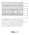
- FIG. 1 is a sectional view for use in describing production of a Bi layer structured ferroelectric thin film according to one embodiment of the present invention.
- a substrate to be used comprises a Si substrate 1, a silicon oxide 2 layer of SiO 2 formed by thermally oxidizing its surface, a lower electrode adhesive layer 3 of Ti on the silicon oxide layer, and a lower electrode 4 of Pt deposited by DC sputtering.
- an underlying base of the Bi layer structured ferroelectric thin film is formed on the surface.
- an oxide buffer layer 5 containing Bi is at first formed. Then, a Bi layer structured ferroelectric substance 6 is stacked on the surface of the buffer layer 5 to form the Bi layer structured ferroelectric thin film.
- a two-layered structure of the Bi layer structured ferroelectric thin film is formed by an additional step of stacking the Bi layer structured ferroelectric substance 6 on the surface of the buffer layer 5.
- a necessary heat treatment is carried out at a temperature not higher than 600°C or 700°C. Such a heat treatment serves to avoid degradation of characteristics in a device element in the Si substrate 1 due to a high temperature.
- the Bi layer structured ferroelectric layer 6 is processed in contact with the surface of the oxide buffer layer 5 containing Bi. As a result, deviation in Bi composition can be avoided within the Bi layer structured ferroelectric thin film thus produced.
- a substrate to be used comprises the Si substrate 1, the silicon oxide 2 layer of "SiO 2 " formed by thermally oxidizing its surface, the lower electrode adhesive layer 3 of Ti on the silicon oxide layer, and the lower electrode 4 of Pt deposited by DC sputtering.
- Sr and Bi as organic metal materials are mixed together at a stoichiometric ratio of SBO.
- the mixed materials are dissolved by an appropriate organic solvent to form the solution.
- organic metal materials containing Sr and Bi alkoxide and organic salt can be used, for example.
- the solvent use may be made of, for instance, 1-methoxy-2-propanol, organic acid, and xylene.
- diisopropoxystrontium and bismuth 2-ethylhexanoate were used as the organic metal materials.
- 2-ethylhexanoic acid and xylene were used. After each of the above-mentioned materials was weighed, these materials were circulated in a dry nitrogen atmosphere at 120°C for one hour. Thus, a coating solution having a concentration of 0.13 mol/kg was obtained.
- this solution was applied on the above-mentioned substrate by a spin coater of 1500 rpm, followed by necessary heat treatments. All of these heat treatments were carried out in an oxygen atmosphere. Specifically, drying of the solvent at 250°C for ten minutes, decomposition and removal of organic components at 400°C for ten minutes, and then crystallization annealing at 600°C or 700°C for one hour were successively carried out.
- FIG. 2 shows X-ray diffraction patterns of the SBO buffer layer after completion of the above-mentioned crystallization annealing.
- the indexed peaks illustrated in the figure may be considered from their positions as occurrence of crystallization of SBO. It is understood that SBO is crystallized by the heat treatment at 600°C or 700°C.
- a subsequent step is to form a thin film by the Bi layer structured ferroelectric substance 6.
- a coating solution to form an SBT thin film is prepared by the use of, for example, alkoxide or organic salt as the organic metal materials of Sr, Bi, and Ta along with the solvent, such as 1-methoxy-2-propanol, organic acid, and xylene.
- Diisopropoxy strontium, pentaethyoxy tantalum, and bismuth 2-ethylhexanoate were used as the organic metal materials.
- 2-ethylhexanoic acid and xylene were used as the solvent. After each of the above-mentioned materials was weighed, these materials were circulated in a dry nitrogen atmosphere at 120°C for one hour. Thus, a coating solution having a concentration of 0.13 mol/kg was obtained.
- this solution was applied on the above-mentioned substrate by a spin coater of 1500 rpm, followed by necessary heat treatments. All of these heat treatments were carried out in oxygen. Specifically, drying of the solvent at 250°C for ten minutes, decomposition and removal of organic components at 650°C for one hour, and then crystallization annealing at 650°C for one hour were successively carried out.
- the application and annealing processes of the SBO thin film as the buffer layer 5, and the application and annealing processes of the SBT thin film of the Bi layer structured ferroelectric substance 6 may be repeated a plurality of times until a desired thickness is achieved. In this manner, each time when the SBT thin film layer is formed, the SBO buffer layer 5 is formed prior to formation of the SBT thin film layer. Thus, an effective influence of each SBO buffer layer 5 is given to each SBT thin film layer.
- FIG. 3 shows an X-ray diffraction pattern of the SBT thin film obtained by the above-mentioned steps and that of the SBT thin film produced without the SBO buffer layer.
- a peak which may specify a fluorite phase is observed when the SBO buffer is absent.
- this phase is a paraelectric phase and does not exhibit ferroelectric characteristics.
- No peak is observed at the position corresponding to SBT of a Bi layer structured perovskite structure which has ferroelectricity. Therefore, a ferroelectric thin film is not obtained as desired.
- the SBO buffer layer is inserted, a peak is observed at the position corresponding to SBT of the Bi layer structured perovskite structure, which is a ferroelectric phase. It is, therefore, understood that the goal of a ferroelectric thin film can be obtained.
- the SBO buffer layer enhances the production of the Bi layer structured perovskite phase as the ferroelectric phase of the SBT.
- the structure of the crystal grain of the SBT thin film thus produced can be described as follows.
- columnar grains (crystalline state) having a grain size of about 0.1-0.2 ⁇ m were uniformly produced throughout the film surface.
- voids within the thin film are decreased.
- a second example will be described here with reference to FIG. 1.
- the concentration of the coating solution for the SBO buffer layer 5 was changed from 0.13 mol/kg of Example 1 to 0.02 mol/kg, and annealing for crystallization was carried out at 700°C. As a result, a SBO thin film having a thickness of about two nm was obtained as the buffer layer 5.
- FIG. 4 shows an X-ray diffraction pattern when the SBT thin film was produced on the SBO buffer layer 5 in a manner similar to that described in Example 1.
- the SBT thin film of the Bi layer structured perovskite structure is crystallized like in the above-mentioned first example.
- the crystallization of the Bi layer structured perovskite phase of the SBT thin film is enhanced.
- FIG. 5 shows a typical P-E hysteresis curve obtained when electrodes are formed on the surface of the thin film thus obtained and a sine wave of ⁇ 5 volts is applied therebetween.
- the crystal grain structure of the SBT thin film was not different from that of Example 1, in which the thickness of the SBO buffer layer was about 60 nm. It is noted that the leakage current density was reduced in comparison with that of the SBT thin film without the SBO buffer layer, listed under "Ref" in Table 1.
- a third example is described here with reference to FIG. 1.
- Annealing for crystallization was carried out at 600°C, instead of 700°C as in Example 2, and the concentration of the coating solution for the SBO buffer layer 5 was equal to 0.02 mol/kg.
- the SBO thin film obtained as the buffer layer 5 had a thickness of about two nm, as in Example 2.
- the SBT thin film was formed on the SBO buffer layer in the manner similar to that described in Example 1, the SBT thin film of the Bi layer structured perovskite structure was crystallized as in Example 2. It is, therefore, obvious that the crystallization of the BI layer structured perovskite phase of the SBT thin film was enhanced.
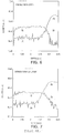
- FIGS. 6 and 7 show analysis results of the composition in depth direction in the SBT thin film structure with the SBO buffer layer produced in this example and in the SBT thin film structure formed on a Pt substrate at 800°C by a conventional method, respectively.
- the sample had a residual polarization of 4.0 ⁇ C/cm 2 measured at five volts.
- the residual polarization value is lower as compared with the case where the crystallization annealing of the SBO buffer layer was carried out at a temperature of 700°C, it is obvious that the SBT thin film produced by the method of this example exhibits ferroelectricity.
- the crystal grain structure of the SBT thin film is substantially identical with that of Example 1, in which the SBO buffer layer had a thickness of 60 nm.
- the Bi layer structured ferroelectric substance 6 is formed by RF ("radio frequency") magnetron sputtering on the substrate, after formation of the SBO buffer layer 5 thereon by the MOD method, as described in Example 3.
- RF radio frequency
- the entire thin film can be crystallized at once, unlike the production by the MOD method. Therefore, as shown in FIG. 8, the SBO buffer layer 5 was able to be applied and baked only once on Pt formed on the substrate as the lower electrode 4. Therefore, the total thickness of the SBO buffer layer 5 was about two nm.
- the thin film obtained in this example had a residual polarization value of 5.1 ⁇ C/cm 2 .
- the ferroelectricity is clearly improved in comparison with the residual polarization value of 0.5 ⁇ C/cm 2 entered in Table 1 under "Ref" for the SBT thin film formed by MOD without the SBO buffer layer.
- BIT Bi 4 Ti 3 O 12
- the Bi layer structured ferroelectric thin film was formed by MOD using BIT and SBT as the buffer layer 5 and the Bi layer structured ferroelectric substance 6, respectively.
- Ti and Bi as organic metal materials mixed in a stoichiometric composition of BIT were dissolved by an appropriate organic solvent to form the BIT solution.
- organic metal materials for example, alkoxide and organic salt can be used.
- solvent use may be made of, for instance, 1-methoxy-2-propanol, organic acid and xylene.
- tetraisopropoxy titanium and bismuth 2-ethylhexanoate were used as organic metal materials, while 2-ethylhexanoic acid and xylene were used as solvents.
- This solution was applied as the buffer layer 5 on Pt formed as the lower electrode 4 of the substrate in FIG. 1 by a spin coater rotated at 1500 rpm, followed by necessary heat treatments. All of these heat treatments were carried out in an oxygen atmosphere. Specifically, drying of the solvent at 250°C for ten minutes, decomposition and removal of organic components at 400°C for ten minutes, and then crystallization annealing at 600°C for one hour were successively carried out. The resulting BIT buffer layer 5 was about seven nm thick.
- the SBT thin film was formed in a manner similar to that described in Example 1. This process was repeated twice together with the BIT deposition process. As a result, the BIT buffer layer had a total thickness of about 14 nm and the layer structure had a total thickness of about 210 nm.
- the capacitor had a residual polarization value of 4.5 ⁇ C/cm 2 . Therefore, it is obvious that the BIT buffer layer functions to enhance the crystallization of the Bi layer structured perovskite phase of the SBT, like the SBO buffer layer. Because the BIT buffer layer has a crystalline Bi layer structured perovskite structure as in SBT, the crystalline structure of the BIT is similar to that of the SBT and is also helpful to enhance the crystallization of SBT.
- the relative dielectric constant (120-140) is greater than that of the SBO buffer layer. Therefore, the ferroelectricity of the layer structure is not degraded, even if the thickness of the buffer layer becomes thick.
- the SBT thin film is composed of uniform and fine columnar grains having a diameter of about 0.1-0.2 ⁇ m.
- the BIT buffer layer 5 is formed by RF magnetron sputtering on Pt formed as the lower electrode 4 of the substrate of FIG. 1, as described in Example 5.
- the Bi layer structured ferroelectric thin film was formed by depositing the Bi layer structured ferroelectric substance 6 on the BIT buffer layer 5 of FIG. 1 using the MOD method.
- the production conditions are the same as in Example 1.
- the process of producing the BIT buffer layer arid the process of producing the Bi layer structured ferroelectric thin film using the MOD method with heat treatment for SBT crystallization were carried out twice.
- the BIT buffer layer measured had a total thickness of about ten nm, while the layer structure measured a total thickness of about 210 nm.
- the capacitor had a residual polarization value of 4.0 ⁇ C/cm 2 . Therefore, it is obvious that the BIT buffer layer formed by sputtering functions to enhance the crystallization of the Bi layer structured perovskite phase in the SBT thin film, similar to the BIT buffer layer formed by MOD.
- the crystal grain structure of the SBT thin film is similar to that of the SBT thin film on the BIT buffer layer formed by MOD, except that the crystal grain size is slightly smaller.
- This seventh example is described with reference to FIG. 9.
- a layer 9 of conductive-oxide forming metal is formed on the uppermost surface of the substrate on which the Bi layer structured ferroelectric thin film is to be formed on the surface of the oxide buffer layer 5 containing Bi.
- Ru ruthenium
- the conductive oxide forming metal 9 which can be used may be Ir or the like.
- the following steps were carried out in order to electrically connect the uppermost surface of the substrate to the Si substrate 1.
- the Si oxide layer 2 of SiO 2 was formed on the Si substrate 1.
- a contact hole was formed in the Si oxide film 2, a diffusion layer was formed.
- the contact hole was filled with polycrystalline Si 7.
- this polycrystalline Si 7 was etched by an etch back technique.
- Ti as the lower electrode adhesive layer 3, TiN layer 8, and Ru formed as the conductive oxide forming metal 9 were successively deposited by sputtering to 20 nm, 50 nm, and 50 nm thickness, respectively.
- the highest temperature of the heat treatment in oxygen atmosphere was 650°C.
- diffusion of oxygen from the surface inwards is prevented in the TiN layer 8 and the Ru layer as the conductive oxide forming metal 9. Therefore, the surface of the polycrystalline Si 7 or the TiN layer 8 is not oxidized. It is consequently possible to electrically connect the diffusion layer of the Si substrate 1 to the conductive oxide forming metal 9 of Ru formed on the uppermost surface of the substrate.
- the diffusion of Ru towards the inside of the Bi layer structured ferroelectric thin film 6 often becomes a problem when the thin film of the Bi layer structured ferroelectric substance 6 is formed on the surface of the conductive oxide forming metal 9 of Ru.
- such diffusion causes no problem at the temperature of 600°C at which the SBO buffer layer 5 is crystallized.
- the SBO buffer layer 5 serves as a barrier layer against the conductive oxide forming metal 9 of Ru, and thus prevents Ru from diffusing into SBT formed as the Bi layer structured ferroelectric substance 6. Accordingly, the characteristics of the Bi layer structured ferroelectric thin film are not degraded.
- the structure in this seventh example had a residual polarization value of 3.8 ⁇ C/cm 2 , which approximates that obtained in Example 3.
- a metal oxide layer 10 is formed on the uppermost surface of the substrate on which the Bi layer structured ferroelectric thin film is to be formed on the surface of the oxide buffer layer 5 containing Bi.
- ruthenium oxide, "RuO 2 " served as conductive oxide 10.
- RuO 2 served as conductive oxide 10.
- IrO 2 or the like may be used as the conductive oxide 10.
- sputtering was conducted to form Ru, as the conductive oxide forming metal 9, on the uppermost surface of the substrate, as in Example 7. Then a subsequent step was conducted by the use of reactive sputtering to further form "RuO 2 ", as the conductive oxide 10, on the above-mentioned surface.
- the SBO buffer layer 5 serves as a barrier layer against Ru and thus prevents Ru from diffusing into SBT formed as the Bi layer structured ferroelectric substance 6. Accordingly, the characteristics of the Bi layer structured ferroelectric thin film are not degraded.
- the structure in this example had a residual polarization value of 3.7 ⁇ C/cm 2 , which approximates that obtained in Example 3.
- Example 1 2 3 4 5 6 7 8 Ref Substrate Pt/Ti Pt/Ti Pt/Ti Pt/Ti Pt/Ti Pt/Ti Pt/Ti Ru RuO 2 Pt/Ti Buffer layer SBO SBO SBO SBO BIT BIT SBO SBO - Buffer layer producing method MOD MOD MOD MOD MOD SP MOD MOD MOD - Buffer layer preparation temperature (°C) 600/ 700 700 600 600 600 600 600 600 - Thickness of buffer layer (nm) 60 4 4 2 14 10 4 4 - Bi layer structured ferroelectric substance SBT SBT SBT SBT SBT SBT SBT SBT SBT SBT SBT SBT SBT SBT SBT SBT SBT SBT SBT SBT SBT SBT SBT SBT Producing method of Bi layer structured ferroelectric substance MOD MOD MOD SP MOD MOD MOD MOD MOD MOD MOD MOD MOD MOD Residual polarization ( ⁇ C/cm 2 )@5V 0 4.2 4.0 5.1 4.5 4.0 3.8 3.7
- SBO or BIT and SBT are used as the buffer layer and the Bi layer structured ferroelectric substance, respectively. It will be noted that a similar effect can be achieved by using BiTaO 4 as the buffer layer, and SrBi 2 Nb 2 O 9 , SrBi 2 (Nb 1 Ta 1 )O 9 , (Sr 0.9 Pb 0.1 )Bi 2 Ta 2 O 9 , or (Sr 0.9 Ba 0.1 )Bi 2 Ta 2 O 9 as the Bi layer structured ferroelectric substance.
- the buffer layer and the Bi layer structured ferroelectric layer use may be made of CVD (chemical vapor deposition), or laser ablation, instead of the MOD method and sputtering.
- CVD chemical vapor deposition
- laser ablation instead of the MOD method and sputtering.
- the crystallization temperature of the buffer layer is 600°C or 700°C in the examples described above, it has been confirmed that a similar effect can be achieved by steps of thermally decomposing the organic components after applying the buffer layer, thereafter forming the Bi layer structured ferroelectric thin film, and crystallizing the buffer layer when the Bi layer structured ferroelectric substance is subjected to the crystallization heat treatment.
- the buffer layer formed by the oxide thin film containing Bi is placed on the surface of the substrate and the Bi layer structured ferroelectric substance is deposited on the upper surface of the buffer layer, then to be crystallized.
- Bi contained in the above-mentioned buffer layer serves as a supply source compensating a lack of Bi within the Bi layer structured ferroelectric thin film arising from reaction of Bi with the precious metal of the lower electrode, which is located at a surface part during crystallization, or with the adhesive layer, or with the thermally oxidized Si underneath.
- the buffer layer is crystallized at a temperature not higher than 700°C.
- the reaction of Pt with Bi can be suppressed because the above-mentioned temperature is lower than about 730°C, at which a Bi-Pt compound is formed.
- the buffer layer and the Bi layer structured ferroelectric substance used for the Bi layer structured ferroelectric thin film are similar to each other in composition and structure. Therefore, the buffer layer acts as nucleation sites for crystallization of the Bi layer structured ferroelectric substance. This is effective to enhance the crystallization of the Bi layer structured ferroelectric thin film at a lower temperature and to form the fine grain structure.
- the buffer layer has a thickness not greater than five percent of that of the Bi layer structured ferroelectric thin film and can be used in a capacitor. Furthermore, the constituent elements of the buffer layer are partially similar to the constituent elements of the Bi layer structured ferroelectric substance. Therefore, during the formation of the Bi layer structured ferroelectric thin film, the buffer layer can be crystallized into the Bi layer structured ferroelectric thin film after the buffer layer finishes its role.
- the conductive oxide forming metal or a combination of the conductive oxide and "TiN" can be deposited on polycrystalline Si and serves as a barrier layer against diffusion of oxygen.
- the method of the invention may be used alone or in combination with other methods, devices and compositions intended to inhibit or reverse the detrimental effects of hydrogen degradation.
- the method of the invention is useful to prevent hydrogen degradation regardless of how it is caused. Reducing and other damaging conditions can arise in many circumstances during integrated circuit fabrication; even routine handling of the wafer can result in degradation of electronic properties.
Landscapes
- Engineering & Computer Science (AREA)
- Power Engineering (AREA)
- Computer Hardware Design (AREA)
- Microelectronics & Electronic Packaging (AREA)
- Condensed Matter Physics & Semiconductors (AREA)
- General Physics & Mathematics (AREA)
- Manufacturing & Machinery (AREA)
- Physics & Mathematics (AREA)
- Chemical & Material Sciences (AREA)
- Materials Engineering (AREA)
- Chemical Kinetics & Catalysis (AREA)
- Semiconductor Memories (AREA)
- Inorganic Insulating Materials (AREA)
- Non-Volatile Memory (AREA)
- Inorganic Compounds Of Heavy Metals (AREA)
- Formation Of Insulating Films (AREA)
- Laminated Bodies (AREA)
- Crystals, And After-Treatments Of Crystals (AREA)
Abstract
Description
- The present invention relates to a method of producing, on a substrate, a ferroelectric thin film of a bismuth layer structure, namely, a bismuth (hereinafter "Bi") layer structured ferroelectric thin film represented by (Bi2O2)2+(AmBnOl)2- and, in particular, to a method of producing a Bi layer structured ferroelectric thin film which is capable of compensating and suppressing deviation in composition of the Bi layer structured ferroelectric thin film and which is capable of suppressing degradation in electrical characteristics.
- Generally, various growing methods, such as organic metal solution coating, chemical vapor deposition (hereinafter CVD), and laser ablation, are known as methods of producing a Bi layer structured ferroelectric thin film. Substrates used therein are typically Si (silicon) substrates having an oxidized surface and a thin layer of high-melting-point precious metal, such as Pt (platinum) or Ir (iridium) deposited on the oxidized Si wafer, or having an oxidized Si layer, a thin film of high-melting-point precious metal, and an appropriate adhesive layer interposed therebetween.
- As exemplified in FIG. 11, a conventional method of producing a Bi layer structured ferroelectric thin film directly forms a Bi layer structured ferroelectric
thin film 6 on the upper surface of alower electrode 4 of Pt which overlies anadhesive layer 3 of Ti (titanium) deposited on aSi oxide layer 2. - A typical method for obtaining excellent ferroelectric characteristics in the above-mentioned process is to heat the substrate at a temperature not lower than 750°C during or after growth of the thin film.
- For instance, as described by Watanabe, et. al., in an article entitled "Preparation of Ferroelectric Thin Films of Bismuth Layer Structured Compounds" (Journal of Applied Physics, Volume 34 (1995),
Part 1, No. 9B, pp. 5240-5244), organic metal solution is coated and thereafter fired in an oxygen atmosphere at a temperature of 800°C in a metal-organic decomposition (hereinafter "MOD") method. - Besides, as described by Hironaka, et. al., in an article entitled "Formation of SrBi2Ta2O9 Thin Films by Flash-MOCVD" (Applied Electronics, Technical Meeting on Physical Properties, Nov. 22, 1995, pp. 15-20), thin films are deposited on a substrate by CVD and thereafter post-annealed in an oxygen atmosphere at a temperature of 800°C in a manner similar to that described above.
- In some of the above-mentioned conventional methods of producing a Bi layer structured ferroelectric thin film, the thin films deposited are often subjected to heat treatment to be crystallized. In this case, the resultant Bi layer structured ferroelectric thin film is composed of granular grains and often undesirably includes voids or pores within the thin film. This brings about a problem that the insulation characteristic of the thin film is degraded as compared with other types of ferroelectric thin films.
- In addition, the annealing temperature of the Bi layer structured ferroelectric thin film is not lower than 750°C. This results in problems, such as an interdiffusion between Bi used as a constituent element of the ferroelectric thin film and the precious metal used as the lower electrode, an adhesive layer, or the oxidized Si layer, and it spoils the flatness of the substrate. If device elements are formed in the Si substrate, their characteristics may be degraded due to the interdiffusion.
- Consideration will be given to the case where a capacitor is formed by the use of a Bi layer structured ferroelectric thin film and is electrically connected to the device element formed in the Si substrate by a polycrystalline Si plug. In this case, the surface of the polycrystalline Si is oxidized by the heat treatment in the oxygen atmosphere at the temperature not lower than 750°C. Such oxidization of the surface of the polycrystalline Si makes an electrical connection impossible.
- In order to solve the above-mentioned problems, it is an object of the present invention to provide a method of producing a Bi layer structured ferroelectric thin film which is capable of compensating and suppressing deviation in composition of the Bi layer structured ferroelectric thin film, suppressing degradation in electrical characteristics, and achieving a good electrical connection.
- A feature of the invention is a method of producing a Bi layer structured ferroelectric thin film comprising steps of: providing a substrate; forming a buffer layer of an oxide thin film containing Bi (bismuth) on the substrate; and forming a thin film of a Bi layer structured ferroelectric substance, where the Bi layer structured ferroelectric substance is represented by a chemical formula (Bi2O2)2+(AmBnOl)2-.
- Another feature of the invention is applying a coating of a solution for forming the Bi layer structured ferroelectric substance onto the buffer layer, and then annealing the coating to form the Bi layer structured ferroelectric thin film.
- Another feature of the invention is a buffer layer having a thickness not greater than about five percent of a total combined thickness of a layer structure containing the Bi layer structured ferroelectric thin film and the buffer layer.
- Another feature of the invention is a preparation temperature of the buffer layer that is lower than a preparation temperature of the Bi layer structured ferroelectric thin film. Preferably, a preparation temperature of the Bi layer structured ferroelectric thin film is not higher than about 650°C.
- Another feature of the inventions is a Bi layer structured ferroelectric substance containing constituent elements A and B as represented in the chemical formula (Bi2O2)2+(AmBnOl)2-, wherein the buffer layer is represented by a chemical formula selected from the group consisting of "AxBiyOz" or "BxBiyOz" and the buffer layer contains only the constituent elements of the Bi layer structured ferroelectric substance.
- Another feature of the invention is a thin film of a Bi layer structured ferroelectric substance containing constituent elements A and B as represented in the chemical formula (Bi2O2)2+(AmBnOl)2-, whereby the constituent element A is selected from a group consisting of a combination of Sr(strontium) and Ba (barium) and a combination of Sr and Pb (lead), and the constituent element B is at least one selected from the group consisting of Ta (tantalum) and Nb (niobium), and whereby the buffer layer of an oxide thin film comprises a Bi layer structured ferroelectric substance containing both of said constituent elements A and B.
- Numerous other features; objects and advantages of the invention will become apparent from the following description when read in conjunction with the accompanying drawings.
-
- FIG. 1 is a sectional view for describing preparation of a thin film according to one embodiment of the present invention.
- FIG. 2 is a graph showing X-ray diffraction patterns of the SBO buffer layer according to one embodiment of the present invention.
- FIG. 3 is a graph comparing one example of X-ray diffraction patterns of the SBT thin film according to the present invention with one example of X-ray diffraction patterns of the SBT thin film produced without the SBO buffer layer.
- FIG. 4 is a graph showing one example of an X-ray diffraction pattern of the SBT thin film according to the present invention.
- FIG. 5 is a P-E hysteresis curve of the thin film layer by the thin film process according to the present invention.
- FIG. 6 is a graph showing the depth profile of the composition of an SBT thin film structure produced by the thin film process of the present invention.
- FIG. 7 is a graph showing the depth profile of the composition of an SBT thin film structure formed on a Pt substrate at 800°C by a conventional method.
- FIG. 8 is a sectional view for describing production of the SBT thin film of FIG. 1 by sputtering according to one embodiment of the present invention.
- FIG. 9 is a sectional view for describing another embodiment of the present invention with a substrate structure different from FIG. 1 and FIG. 8.
- FIG. 10 is a sectional view for describing still another embodiment of the present invention with a substrate structure different from FIG. 1, FIG. 8, and FIG. 9.
- FIG. 11 is a sectional view of a conventional example.
-
- It should be understood that the FIGS. 1, 8-10 depicting ferroelectric integrated circuit sections are not meant to be actual cross-sectional views of any particular portion of an actual integrated circuit device. In the actual devices, the layers will not be as regular and their thicknesses may have different proportions. The various layers in actual devices often are curved and possess overlapping edges. The figures instead show idealized representations which are employed to depict more clearly and fully the method of the invention than would otherwise be possible. Likewise, other integrated circuits fabricated using the method of the invention could include other elements and compositions of material.
- According to the present invention, a method of producing a Bi layer structured ferroelectric thin film which is represented by (Bi2O2)2+(AmBnOl)2-comprises the step of forming, on a substrate, a buffer layer composed of an oxide thin film containing Bi (bismuth). In cases where the method comprises the steps of repeatedly applying a Bi layer structured ferroelectric substance onto the substrate by solution coating and annealing the substance to form the Bi layer structured ferroelectric thin film, an additional step may be included to form the buffer layer composed of an oxide thin film containing Bi (bismuth) on the substrate prior to at least one of the solution-applying steps.
- With the above-mentioned structure, crystallization of the thin film progresses from nucleation sites on the surface of a buffer layer composed of an oxide thin film formed in an inner portion adjacent to the substrate. This eliminates occurrence of the voids arising from formation of grains that crystallize from random positions. In addition, Bi included in the buffer layer serves to compensate a reduction of an amount of Bi that is caused to occur as a result of reaction with an underlying electrode, with an interior adhesive layer, or with the Si oxidized layer during crystallization of the Bi layer structured ferroelectric substance.
- It is preferable that a total thickness of the buffer layer comprising at least one layer is not greater than about five percent of a total thickness of the Bi layer structured ferroelectric thin film and the buffer layer. When the thin film of the above-mentioned structure is used as a capacitor, degradation in electrical characteristics caused by insertion of the buffer layer can be suppressed to a minimum.
- Furthermore, it is preferred that a preparation temperature of the buffer layer is lower than that of the Bi layer structured ferroelectric thin film. By crystallizing the buffer layer at a temperature lower than that of the Bi layer structured ferroelectric thin film as described above, it is possible to prevent Bi from diffusing outside of the buffer layer. In addition, the crystallized buffer layer inhibits Bi from diffusing outside during subsequent heat treatment at a higher temperature. Therefore, crystallization of the Bi layer structured ferroelectric substance can be achieved without degradation of flatness and characteristics of the lower electrode, the adhesive layer, and the Si oxidized film due to reaction with Bi. In this case also, the buffer layer serves to provide nucleation sites of crystallization and, therefore, to lower crystallization temperature and to suppress deviation in composition of the Bi layer structured ferroelectrics.
- It is preferable that a preparation temperature of the Bi layer structured ferroelectric thin film is not higher than about 650°C. When the preparation temperature is not higher than 650°C, it is possible to avoid failure of electrical connection resulting from oxidization of polycrystalline Si by depositing titanium nitride (TiN) on the polycrystalline Si as a diffusion barrier layer against oxygen.
- It is preferable that the buffer layer be represented by "AxBiyOz" or "BxBiyOz", which only contain constituent elements included in the Bi layer structured ferroelectrics that are essential components of the Bi layer structured ferroelectric thin film, whereby constituent element A of the Bi layer structured ferroelectric substance is either at least one of Sr (strontium) and Ba (barium) or at least one of Sr and Pb (lead), while the element B is at least one of Ta (tantalum) and Nb (niobium).
- As described above, the constituent elements of the buffer layer include some of the constituent elements of the Bi layer structured ferroelectric substance. With this structure, similarity in composition and crystalline structure between the buffer layer and the Bi layer structured ferroelectric thin film is increased and crystallization energy is lowered. In addition, when the buffer layer is extremely thin in comparison with the Bi layer structured ferroelectric thin film and an appropriate composition of the Bi layer structured ferroelectric thin film is slightly excessive, most of the buffer layer can be crystallized into the Bi layer structured ferroelectric thin film after the role of the buffer layer is finished. In this event, degradation in electric characteristics of a capacitor can be avoided.
- Next, description will be made in detail as regards embodiments of the present invention by reference to the figures.
- FIG. 1 is a sectional view for use in describing production of a Bi layer structured ferroelectric thin film according to one embodiment of the present invention. As shown in FIG. 1, a substrate to be used comprises a
Si substrate 1, asilicon oxide 2 layer of SiO2 formed by thermally oxidizing its surface, a lowerelectrode adhesive layer 3 of Ti on the silicon oxide layer, and alower electrode 4 of Pt deposited by DC sputtering. Thus, an underlying base of the Bi layer structured ferroelectric thin film is formed on the surface. - In order to form the Bi layer structured ferroelectric thin film on the above-mentioned surface, an
oxide buffer layer 5 containing Bi is at first formed. Then, a Bi layer structuredferroelectric substance 6 is stacked on the surface of thebuffer layer 5 to form the Bi layer structured ferroelectric thin film. In case of FIG. 1, a two-layered structure of the Bi layer structured ferroelectric thin film is formed by an additional step of stacking the Bi layer structuredferroelectric substance 6 on the surface of thebuffer layer 5. In this production process, a necessary heat treatment is carried out at a temperature not higher than 600°C or 700°C. Such a heat treatment serves to avoid degradation of characteristics in a device element in theSi substrate 1 due to a high temperature. In addition, the Bi layer structuredferroelectric layer 6 is processed in contact with the surface of theoxide buffer layer 5 containing Bi. As a result, deviation in Bi composition can be avoided within the Bi layer structured ferroelectric thin film thus produced. - Now, a first embodiment of the present invention will be described in detail with reference to FIG. 1.
- As mentioned above, a substrate to be used comprises the
Si substrate 1, thesilicon oxide 2 layer of "SiO2" formed by thermally oxidizing its surface, the lowerelectrode adhesive layer 3 of Ti on the silicon oxide layer, and thelower electrode 4 of Pt deposited by DC sputtering. - The following description will be directed to the case of forming the Bi layer structured ferroelectric thin film. In order to form the Bi layer structured ferroelectric thin film on the above-mentioned surface, "Sr3Bi2O6" (hereinafter "SBO") is first formed by a MOD ("Metal-Organic Decomposition") method as the
oxide buffer layer 5 containing Bi. Then, "SrBi2Ta2O9" (hereinafter "SBT") is formed by the MOD method as the Bi layer structuredferroelectric substance 6 on the surface of thebuffer layer 5. - At a first step, in order to form the
buffer layer 5 of SBO, Sr and Bi as organic metal materials are mixed together at a stoichiometric ratio of SBO. The mixed materials are dissolved by an appropriate organic solvent to form the solution. As the organic metal materials containing Sr and Bi, alkoxide and organic salt can be used, for example. As the solvent, use may be made of, for instance, 1-methoxy-2-propanol, organic acid, and xylene. - In this example, diisopropoxystrontium and bismuth 2-ethylhexanoate were used as the organic metal materials. As the solvent, 2-ethylhexanoic acid and xylene were used. After each of the above-mentioned materials was weighed, these materials were circulated in a dry nitrogen atmosphere at 120°C for one hour. Thus, a coating solution having a concentration of 0.13 mol/kg was obtained.
- At a next step, this solution was applied on the above-mentioned substrate by a spin coater of 1500 rpm, followed by necessary heat treatments. All of these heat treatments were carried out in an oxygen atmosphere. Specifically, drying of the solvent at 250°C for ten minutes, decomposition and removal of organic components at 400°C for ten minutes, and then crystallization annealing at 600°C or 700°C for one hour were successively carried out.
- FIG. 2 shows X-ray diffraction patterns of the SBO buffer layer after completion of the above-mentioned crystallization annealing. The indexed peaks illustrated in the figure may be considered from their positions as occurrence of crystallization of SBO. It is understood that SBO is crystallized by the heat treatment at 600°C or 700°C.
- A subsequent step is to form a thin film by the Bi layer structured
ferroelectric substance 6. A coating solution to form an SBT thin film is prepared by the use of, for example, alkoxide or organic salt as the organic metal materials of Sr, Bi, and Ta along with the solvent, such as 1-methoxy-2-propanol, organic acid, and xylene. - Diisopropoxy strontium, pentaethyoxy tantalum, and bismuth 2-ethylhexanoate were used as the organic metal materials. As the solvent, 2-ethylhexanoic acid and xylene were used. After each of the above-mentioned materials was weighed, these materials were circulated in a dry nitrogen atmosphere at 120°C for one hour. Thus, a coating solution having a concentration of 0.13 mol/kg was obtained.
- At a next step, this solution was applied on the above-mentioned substrate by a spin coater of 1500 rpm, followed by necessary heat treatments. All of these heat treatments were carried out in oxygen. Specifically, drying of the solvent at 250°C for ten minutes, decomposition and removal of organic components at 650°C for one hour, and then crystallization annealing at 650°C for one hour were successively carried out.
- In the above-mentioned sequence of steps, it is possible to form the SBT thin film with a thickness of 90-100 nm. In order to increase the thickness, the above-mentioned sequence of steps were again repeated in a manner depicted in FIG. 1 to accomplish the final thickness of about 250 nm.
- In order to further increase the thickness, the application and annealing processes of the SBO thin film as the
buffer layer 5, and the application and annealing processes of the SBT thin film of the Bi layer structuredferroelectric substance 6 may be repeated a plurality of times until a desired thickness is achieved. In this manner, each time when the SBT thin film layer is formed, theSBO buffer layer 5 is formed prior to formation of the SBT thin film layer. Thus, an effective influence of eachSBO buffer layer 5 is given to each SBT thin film layer. - FIG. 3 shows an X-ray diffraction pattern of the SBT thin film obtained by the above-mentioned steps and that of the SBT thin film produced without the SBO buffer layer. As shown in this figure, a peak which may specify a fluorite phase is observed when the SBO buffer is absent. However, this phase is a paraelectric phase and does not exhibit ferroelectric characteristics. No peak is observed at the position corresponding to SBT of a Bi layer structured perovskite structure which has ferroelectricity. Therefore, a ferroelectric thin film is not obtained as desired. On the other hand, when the SBO buffer layer is inserted, a peak is observed at the position corresponding to SBT of the Bi layer structured perovskite structure, which is a ferroelectric phase. It is, therefore, understood that the goal of a ferroelectric thin film can be obtained.
- From the above-mentioned experimental results, it is obvious that the SBO buffer layer enhances the production of the Bi layer structured perovskite phase as the ferroelectric phase of the SBT. However, because a thickness ratio of the SBO buffer layer and the SBT thin film is as large as 60 nm/200 nm (= 0.3), and a relative dielectric constant (about 15) of SBO as a paraelectric material is small as compared with SBT, residual polarization representative of ferroelectricity was not observed when an electrode was formed on the SBT.
- The structure of the crystal grain of the SBT thin film thus produced can be described as follows. In the SBT thin film on the SRO buffer layer, columnar grains (crystalline state) having a grain size of about 0.1-0.2 µm were uniformly produced throughout the film surface. In comparison with the SBT thin film having no buffer layer and produced at a temperature not lower than 750°C, it is confirmed that voids within the thin film are decreased.
- A second example will be described here with reference to FIG. 1. The concentration of the coating solution for the
SBO buffer layer 5 was changed from 0.13 mol/kg of Example 1 to 0.02 mol/kg, and annealing for crystallization was carried out at 700°C. As a result, a SBO thin film having a thickness of about two nm was obtained as thebuffer layer 5. - FIG. 4 shows an X-ray diffraction pattern when the SBT thin film was produced on the
SBO buffer layer 5 in a manner similar to that described in Example 1. - As illustrated in the figure, even though the total thickness of the SBO buffer layer of this example is as small as about 4 nm, the SBT thin film of the Bi layer structured perovskite structure is crystallized like in the above-mentioned first example. Thus, it is obvious that the crystallization of the Bi layer structured perovskite phase of the SBT thin film is enhanced.
- FIG. 5 shows a typical P-E hysteresis curve obtained when electrodes are formed on the surface of the thin film thus obtained and a sine wave of ± 5 volts is applied therebetween. As shown in Table 1 below, a thickness ratio of the SBO buffer layer and the SBT thin film is as small as 4 nm/200 nm (= 0.02). Therefore, only a slight influence is given to the electrical characteristics by the SBO buffer layer having a small relative dielectric constant. Thus, a hysteresis showing ferroelectric characteristics can be clearly observed. From the result of the measurement, a residual polarization value of this sample is obtained as 4.2 µC/cm2.
- The crystal grain structure of the SBT thin film was not different from that of Example 1, in which the thickness of the SBO buffer layer was about 60 nm. It is noted that the leakage current density was reduced in comparison with that of the SBT thin film without the SBO buffer layer, listed under "Ref" in Table 1.
- A third example is described here with reference to FIG. 1. Annealing for crystallization was carried out at 600°C, instead of 700°C as in Example 2, and the concentration of the coating solution for the
SBO buffer layer 5 was equal to 0.02 mol/kg. As a result, the SBO thin film obtained as thebuffer layer 5 had a thickness of about two nm, as in Example 2. - When the SBT thin film was formed on the SBO buffer layer in the manner similar to that described in Example 1, the SBT thin film of the Bi layer structured perovskite structure was crystallized as in Example 2. It is, therefore, obvious that the crystallization of the BI layer structured perovskite phase of the SBT thin film was enhanced.
- FIGS. 6 and 7 show analysis results of the composition in depth direction in the SBT thin film structure with the SBO buffer layer produced in this example and in the SBT thin film structure formed on a Pt substrate at 800°C by a conventional method, respectively.
- In the structure produced by the method based on this example shown in FIG. 6, a boundary surface between the Pt surface of the substrate and the SBT thin film composed of the ferroelectric substance and the buffer layer is sharp, and no substantial diffusion of Bi into Pt is observed. On the other hand, in the conventional method without the buffer layer, shown in FIG. 7, diffusion of Bi into the Pt layer is observed. From the results of the composition analysis, the SBO buffer layer did not remain as a distinct layer.
- As shown in Table 1 below, the sample had a residual polarization of 4.0 µC/cm2 measured at five volts. Although the residual polarization value is lower as compared with the case where the crystallization annealing of the SBO buffer layer was carried out at a temperature of 700°C, it is obvious that the SBT thin film produced by the method of this example exhibits ferroelectricity. Besides, the crystal grain structure of the SBT thin film is substantially identical with that of Example 1, in which the SBO buffer layer had a thickness of 60 nm.
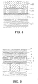
- A fourth example will be described here with reference to FIG. 8. In this example, the Bi layer structured
ferroelectric substance 6 is formed by RF ("radio frequency") magnetron sputtering on the substrate, after formation of theSBO buffer layer 5 thereon by the MOD method, as described in Example 3. - A target comprised ceramics having a composition of "Sr/Bi/Ta = 1/2.5/2" in mole ratio. Typical sputtering conditions were: RF power of 500 W, gas pressure of 40 mTorr, gas composition ratio of"Ar/O2 = 9/1", and no heating of the substrate. Under these conditions, an SBT thin film of about 200 nm was formed. After deposition of the film, post-annealing was carried out at 650°C for one hour in an oxygen atmosphere.
- In the SBT thin film produced by sputtering, the entire thin film can be crystallized at once, unlike the production by the MOD method. Therefore, as shown in FIG. 8, the
SBO buffer layer 5 was able to be applied and baked only once on Pt formed on the substrate as thelower electrode 4. Therefore, the total thickness of theSBO buffer layer 5 was about two nm. - The thin film obtained in this example had a residual polarization value of 5.1 µC/cm2. Thus, the ferroelectricity is clearly improved in comparison with the residual polarization value of 0.5 µC/cm2 entered in Table 1 under "Ref" for the SBT thin film formed by MOD without the SBO buffer layer.
- In this fifth example, "Bi4Ti3O12" (hereinafter"BIT") is used as the
oxide buffer layer 5 containing Bi shown in FIG. 1. BIT is a type of Bi layer structured ferroelectrics. - The Bi layer structured ferroelectric thin film was formed by MOD using BIT and SBT as the
buffer layer 5 and the Bi layer structuredferroelectric substance 6, respectively. - First, Ti and Bi as organic metal materials mixed in a stoichiometric composition of BIT were dissolved by an appropriate organic solvent to form the BIT solution. As the organic metal materials comprising Ti and Bi, for example, alkoxide and organic salt can be used. As the solvent, use may be made of, for instance, 1-methoxy-2-propanol, organic acid and xylene.
- In the BIT solution of this example, tetraisopropoxy titanium and bismuth 2-ethylhexanoate were used as organic metal materials, while 2-ethylhexanoic acid and xylene were used as solvents.
- After each of the materials was weighed, these materials were circulated in a dry nitrogen atmosphere at 120°C for one hour. Thus, a coating solution having a concentration of 0.013 mol/kg was obtained.
- This solution was applied as the
buffer layer 5 on Pt formed as thelower electrode 4 of the substrate in FIG. 1 by a spin coater rotated at 1500 rpm, followed by necessary heat treatments. All of these heat treatments were carried out in an oxygen atmosphere. Specifically, drying of the solvent at 250°C for ten minutes, decomposition and removal of organic components at 400°C for ten minutes, and then crystallization annealing at 600°C for one hour were successively carried out. The resultingBIT buffer layer 5 was about seven nm thick. - The SBT thin film was formed in a manner similar to that described in Example 1. This process was repeated twice together with the BIT deposition process. As a result, the BIT buffer layer had a total thickness of about 14 nm and the layer structure had a total thickness of about 210 nm.
- As listed in Table 1, the capacitor had a residual polarization value of 4.5 µC/cm2. Therefore, it is obvious that the BIT buffer layer functions to enhance the crystallization of the Bi layer structured perovskite phase of the SBT, like the SBO buffer layer. Because the BIT buffer layer has a crystalline Bi layer structured perovskite structure as in SBT, the crystalline structure of the BIT is similar to that of the SBT and is also helpful to enhance the crystallization of SBT.
- In case of the BIT buffer layer, the relative dielectric constant (120-140) is greater than that of the SBO buffer layer. Therefore, the ferroelectricity of the layer structure is not degraded, even if the thickness of the buffer layer becomes thick. Moreover, the SBT thin film is composed of uniform and fine columnar grains having a diameter of about 0.1-0.2 µm.
- In this sixth example, the
BIT buffer layer 5 is formed by RF magnetron sputtering on Pt formed as thelower electrode 4 of the substrate of FIG. 1, as described in Example 5. - With respect to the BIT buffer layer, typical sputtering conditions are: a sputter target composition ratio of "Bi/Ti = 1/1"; RF power of 250 W; gas pressure of 40 mTorr; gas composition ratio of"Ar/O2 = 9/1"; and no heating of the substrate. Under these conditions, by carrying out the crystallization annealing at 600°C for one hour after sputtering, a BIT buffer layer with a thickness of five nm was formed.
- The Bi layer structured ferroelectric thin film was formed by depositing the Bi layer structured
ferroelectric substance 6 on theBIT buffer layer 5 of FIG. 1 using the MOD method. The production conditions are the same as in Example 1. - In this case, the process of producing the BIT buffer layer arid the process of producing the Bi layer structured ferroelectric thin film using the MOD method with heat treatment for SBT crystallization were carried out twice. The BIT buffer layer measured had a total thickness of about ten nm, while the layer structure measured a total thickness of about 210 nm.
- As shown in Table 1, under Example 6, the capacitor had a residual polarization value of 4.0 µC/cm2. Therefore, it is obvious that the BIT buffer layer formed by sputtering functions to enhance the crystallization of the Bi layer structured perovskite phase in the SBT thin film, similar to the BIT buffer layer formed by MOD. The crystal grain structure of the SBT thin film is similar to that of the SBT thin film on the BIT buffer layer formed by MOD, except that the crystal grain size is slightly smaller.
- This seventh example is described with reference to FIG. 9. As depicted in FIG. 9, a
layer 9 of conductive-oxide forming metal is formed on the uppermost surface of the substrate on which the Bi layer structured ferroelectric thin film is to be formed on the surface of theoxide buffer layer 5 containing Bi. In this example, Ru (ruthenium) served as a conductive-oxide forming metal 9. Besides ruthenium, the conductiveoxide forming metal 9 which can be used may be Ir or the like. - In this seventh example, the following steps were carried out in order to electrically connect the uppermost surface of the substrate to the
Si substrate 1. First, theSi oxide layer 2 of SiO2 was formed on theSi substrate 1. After a contact hole was formed in theSi oxide film 2, a diffusion layer was formed. The contact hole was filled withpolycrystalline Si 7. - Then, this
polycrystalline Si 7 was etched by an etch back technique. On an exposed surface, Ti as the lowerelectrode adhesive layer 3,TiN layer 8, and Ru formed as the conductiveoxide forming metal 9 were successively deposited by sputtering to 20 nm, 50 nm, and 50 nm thickness, respectively. - In this example, the highest temperature of the heat treatment in oxygen atmosphere was 650°C. Thus, diffusion of oxygen from the surface inwards is prevented in the
TiN layer 8 and the Ru layer as the conductiveoxide forming metal 9. Therefore, the surface of thepolycrystalline Si 7 or theTiN layer 8 is not oxidized. It is consequently possible to electrically connect the diffusion layer of theSi substrate 1 to the conductiveoxide forming metal 9 of Ru formed on the uppermost surface of the substrate. - The diffusion of Ru towards the inside of the Bi layer structured ferroelectric
thin film 6 often becomes a problem when the thin film of the Bi layer structuredferroelectric substance 6 is formed on the surface of the conductiveoxide forming metal 9 of Ru. However, such diffusion causes no problem at the temperature of 600°C at which theSBO buffer layer 5 is crystallized. As a result, theSBO buffer layer 5 serves as a barrier layer against the conductiveoxide forming metal 9 of Ru, and thus prevents Ru from diffusing into SBT formed as the Bi layer structuredferroelectric substance 6. Accordingly, the characteristics of the Bi layer structured ferroelectric thin film are not degraded. - The structure in this seventh example had a residual polarization value of 3.8 µC/cm2, which approximates that obtained in Example 3.
- This eighth example is described with reference to FIG. 10. In FIG. 10, a
metal oxide layer 10 is formed on the uppermost surface of the substrate on which the Bi layer structured ferroelectric thin film is to be formed on the surface of theoxide buffer layer 5 containing Bi. In this example, ruthenium oxide, "RuO2", served asconductive oxide 10. Besides RuO2, "IrO2" or the like may be used as theconductive oxide 10. - In this example, sputtering was conducted to form Ru, as the conductive
oxide forming metal 9, on the uppermost surface of the substrate, as in Example 7. Then a subsequent step was conducted by the use of reactive sputtering to further form "RuO2", as theconductive oxide 10, on the above-mentioned surface. - In this example, diffusion of oxygen is prevented in the
TiN layer 8 and the RuO2 layer, as in Example 7. Further, theSBO buffer layer 5 serves as a barrier layer against Ru and thus prevents Ru from diffusing into SBT formed as the Bi layer structuredferroelectric substance 6. Accordingly, the characteristics of the Bi layer structured ferroelectric thin film are not degraded. - The structure in this example had a residual polarization value of 3.7 µC/cm2, which approximates that obtained in Example 3.
- In Table 1, values of experimental measurements of Examples 1-8 are listed for comparison with the conventional example ("Ref") with respect to materials, production methods, and characteristics.
Example 1 2 3 4 5 6 7 8 Ref Substrate Pt/Ti Pt/Ti Pt/Ti Pt/Ti Pt/Ti Pt/Ti Ru RuO2 Pt/Ti Buffer layer SBO SBO SBO SBO BIT BIT SBO SBO - Buffer layer producing method MOD MOD MOD MOD MOD SP MOD MOD - Buffer layer preparation temperature (°C) 600/ 700 700 600 600 600 600 600 600 - Thickness of buffer layer (nm) 60 4 4 2 14 10 4 4 - Bi layer structured ferroelectric substance SBT SBT SBT SBT SBT SBT SBT SBT SBT Producing method of Bi layer structured ferroelectric substance MOD MOD MOD SP MOD MOD MOD MOD MOD Residual polarization (µC/cm2)@ 5V 0 4.2 4.0 5.1 4.5 4.0 3.8 3.7 0.5 Leak current density (A/cm2)@5V - 1E 1E 4E 3E 2E 4E 4E 3E -7 -7 -7 -7 -7 -7 -7 -7 - In the foregoing description, SBO or BIT and SBT are used as the buffer layer and the Bi layer structured ferroelectric substance, respectively. It will be noted that a similar effect can be achieved by using BiTaO4 as the buffer layer, and SrBi2Nb2O9, SrBi2(Nb1Ta1)O9, (Sr0.9Pb0.1)Bi2Ta2O9, or (Sr0.9Ba0.1)Bi2Ta2O9 as the Bi layer structured ferroelectric substance.
- As a method of forming thin films of the buffer layer and the Bi layer structured ferroelectric layer, use may be made of CVD (chemical vapor deposition), or laser ablation, instead of the MOD method and sputtering. Further, although the crystallization temperature of the buffer layer is 600°C or 700°C in the examples described above, it has been confirmed that a similar effect can be achieved by steps of thermally decomposing the organic components after applying the buffer layer, thereafter forming the Bi layer structured ferroelectric thin film, and crystallizing the buffer layer when the Bi layer structured ferroelectric substance is subjected to the crystallization heat treatment.
- As described above, the following effects can be achieved according to the present invention.
- As a first effect, it is possible to suppress deviation in composition of the Bi layer structured ferroelectric thin film and to avoid degradation in characteristics.
- Specifically, the buffer layer formed by the oxide thin film containing Bi is placed on the surface of the substrate and the Bi layer structured ferroelectric substance is deposited on the upper surface of the buffer layer, then to be crystallized. With this structure, Bi contained in the above-mentioned buffer layer serves as a supply source compensating a lack of Bi within the Bi layer structured ferroelectric thin film arising from reaction of Bi with the precious metal of the lower electrode, which is located at a surface part during crystallization, or with the adhesive layer, or with the thermally oxidized Si underneath. Thus, crystallization of the Bi layer structured ferroelectric substance is promoted while deviation in composition is suppressed. Moreover, the buffer layer is crystallized at a temperature not higher than 700°C. Therefore, in a case where the Pt layer is directly contacted with the buffer layer containing Bi, the reaction of Pt with Bi can be suppressed because the above-mentioned temperature is lower than about 730°C, at which a Bi-Pt compound is formed.
- As a second effect, the crystallization of the Bi layer structured ferroelectric thin film progresses at a lower temperature, which brings about the first effect.
- Specifically, the buffer layer and the Bi layer structured ferroelectric substance used for the Bi layer structured ferroelectric thin film are similar to each other in composition and structure. Therefore, the buffer layer acts as nucleation sites for crystallization of the Bi layer structured ferroelectric substance. This is effective to enhance the crystallization of the Bi layer structured ferroelectric thin film at a lower temperature and to form the fine grain structure.
- As a third effect, it is possible to minimize or avoid degradation of electrical characteristics required in a capacitor. The reason is because the buffer layer has a thickness not greater than five percent of that of the Bi layer structured ferroelectric thin film and can be used in a capacitor. Furthermore, the constituent elements of the buffer layer are partially similar to the constituent elements of the Bi layer structured ferroelectric substance. Therefore, during the formation of the Bi layer structured ferroelectric thin film, the buffer layer can be crystallized into the Bi layer structured ferroelectric thin film after the buffer layer finishes its role.
- As a fourth effect, it is possible to prevent failure of electrical connection caused by oxidizing polycrystalline Si. When the deposition temperature is not higher than 650°C, the conductive oxide forming metal or a combination of the conductive oxide and "TiN" can be deposited on polycrystalline Si and serves as a barrier layer against diffusion of oxygen.
- The method of the invention may be used alone or in combination with other methods, devices and compositions intended to inhibit or reverse the detrimental effects of hydrogen degradation. The method of the invention is useful to prevent hydrogen degradation regardless of how it is caused. Reducing and other damaging conditions can arise in many circumstances during integrated circuit fabrication; even routine handling of the wafer can result in degradation of electronic properties.
- There has been described a method for fabricating ferroelectric integrated circuits that permits exposure to hydrogen and still results in ferroelectric devices with good electrical properties. It should be understood that the particular embodiments shown in the drawings and described within this specification are for purposes of example and should not be construed to limit the invention which will be described in the claims below. Further, it is evident that those skilled in the art may now make numerous uses and modifications of the specific embodiments described, without departing from the inventive concepts. It is also evident that the steps recited may in some instances be performed in a different order; or equivalent structures and processes may be substituted for the various structures and processes described. Consequently, the invention is to be construed as embracing each and every novel feature and novel combination of features present in and/or possessed by the fabrication processes and electronic structures described.
Claims (14)
- A method of producing a Bi layer structured ferroelectric thin film, comprising steps of:providing a substrate;forming a buffer layer of an oxide thin film containing Bi (bismuth) on said substrate; andthereafter forming a thin film of a Bi layer structured ferroelectric substance on said buffer layer, said Bi layer structured ferroelectric substance represented by a chemical formula (Bi2O2)2+(AmBnOl)2-.
- A method of producing a Bi layer structured ferroelectric thin film as in claim 1, wherein said steps of forming a buffer layer and of thereafter forming a thin film of a Bi layer structured ferroelectric substance on said buffer layer are conducted more than one time.
- A method of producing a Bi layer structured ferroelectric thin film as in claim 1, wherein said buffer layer has a thickness not greater than about five percent of a total combined thickness of a layer structure containing said Bi layer structured ferroelectric thin film and said buffer layer.
- A method of producing a Bi layer structured ferroelectric thin film as in claim 1, wherein a preparation temperature of said buffer layer is lower than a preparation temperature of said Bi layer structured ferroelectric thin film.
- A method of producing a Bi layer structured ferroelectric thin film as in claim 1, wherein a preparation temperature of said Bi layer structured ferroelectric thin film is not higher than about 650°C.
- A method of producing a Bi layer structured ferroelectric thin film as in claim 1,
wherein said Bi layer structured ferroelectric substance contains constituent elements A and B as represented in said chemical formula (Bi2O2)2+(AmBnOl)2-; and
wherein said buffer layer is represented by a chemical formula selected from the group consisting of "AxBiyOz" or "BxBiyOz" and said buffer layer contains only said constituent elements of said Bi layer structured ferroelectric substance. - A method of producing a Bi layer structured ferroelectric thin film as in claim 1,
wherein said thin film of a Bi layer structured ferroelectric substance contains constituent elements A and B as represented in said chemical formula (Bi2O2)2+(AmBnOl)2-;
whereby said constituent element A is selected from a group consisting of a combination of Sr (strontium) and Ba (barium) and a combination of Sr and Pb (lead);
whereby said constituent element B is at least one selected from the group consisting of Ta (tantalum) and Nb (niobium); and
whereby said buffer layer of an oxide thin film comprises a Bi layer structured ferroelectric substance containing both of said constituent elements A and B. - A method of producing a Bi layer structured ferroelectric thin film, comprising steps of:providing a substrate;forming a buffer layer of an oxide thin film containing Bi (bismuth) on said substrate;applying onto said buffer layer a coating of a solution for forming a Bi layer structured ferroelectric substance; andannealing said coating to form said Bi layer structured ferroelectric thin film containing said Bi layer structured ferroelectric substance, said Bi layer structured ferroelectric substance represented by a chemical formula (Bi2O2)2+(AmBnOl)2-.
- A method of producing a Bi layer structured ferroelectric thin film as in claim 8, wherein said buffer layer has a thickness not greater than about five percent of a total combined thickness of a layer structure containing said Bi layer structured ferroelectric thin film and said buffer layer.
- A method of producing a Bi layer structured ferroelectric thin film as in claim 8, wherein a preparation temperature of said buffer layer is lower than a preparation temperature of said Bi layer structured ferroelectric thin film.
- A method of producing a Bi layer structured ferroelectric thin film as in claim 8, wherein a preparation temperature of said Bi layer structured ferroelectric thin film is not higher than about 650°C.
- A method of producing a Bi layer structured ferroelectric thin film as in claim 8,
wherein said Bi layer structured ferroelectric substance contains constituent elements A and B as represented in said chemical formula (Bi2O2)2+(AmBnOl)2-; and
wherein said buffer layer is represented by a chemical formula selected from the group consisting of "AxBiyOz" or "BxBiyOz" and said buffer layer contains only said constituent elements of said Bi layer structured ferroelectric substance. - A method of producing a Bi layer structured ferroelectric thin film as in claim 8,
wherein said thin film of a Bi layer structured ferroelectric substance contains constituent elements A and B as represented in said chemical formula (Bi2O2)2+(AmBnOl)2-;
whereby said constituent element A is selected from a group consisting of a combination of Sr (strontium) and Ba (barium) and a combination of Sr and Pb (lead);
whereby said constituent element B is at least one selected from the group consisting of Ta (tantalum) and Nb (niobium); and
whereby said buffer layer of an oxide thin film comprises a Bi layer structured ferroelectric substance containing both of said constituent elements A and B. - A method of producing a Bi layer structured ferroelectric thin film as in claim 8, wherein said steps of forming a buffer layer, of applying onto said buffer layer a coating and of annealing said coating are repeated.
Applications Claiming Priority (3)
| Application Number | Priority Date | Filing Date | Title |
|---|---|---|---|
| JP28153197A JP3549715B2 (en) | 1997-10-15 | 1997-10-15 | Method for producing Bi layered ferroelectric thin film |
| JP281531/97 | 1997-10-15 | ||
| JP28153197 | 1997-10-15 |
Publications (2)
| Publication Number | Publication Date |
|---|---|
| EP0910120A2 true EP0910120A2 (en) | 1999-04-21 |
| EP0910120A3 EP0910120A3 (en) | 2000-02-02 |
Family
ID=17640480
Family Applications (1)
| Application Number | Title | Priority Date | Filing Date |
|---|---|---|---|
| EP98119403A Withdrawn EP0910120A3 (en) | 1997-10-15 | 1998-10-14 | Method of producing a ferroelectric thin film containing bismuth |
Country Status (5)
| Country | Link |
|---|---|
| US (1) | US6194227B1 (en) |
| EP (1) | EP0910120A3 (en) |
| JP (1) | JP3549715B2 (en) |
| KR (1) | KR100478748B1 (en) |
| CN (1) | CN1114577C (en) |
Cited By (5)
| Publication number | Priority date | Publication date | Assignee | Title |
|---|---|---|---|---|
| WO2002017365A1 (en) * | 2000-08-24 | 2002-02-28 | Infineon Technologies Ag | Low temperature processing of ferroelectric strontium bismuth tantalate layers and the production of ferroelectric components thereof |
| US6495878B1 (en) | 1999-08-02 | 2002-12-17 | Symetrix Corporation | Interlayer oxide containing thin films for high dielectric constant application |
| WO2003005433A2 (en) * | 2001-07-03 | 2003-01-16 | Matsushita Electric Industrial Co., Ltd. | Integrated circuit device including a layered superlattice material with an interface buffer layer |
| WO2004075296A1 (en) * | 2003-02-19 | 2004-09-02 | Fujitsu Limited | Method for manufacturing ferroelectric capacitor |
| US7312514B2 (en) | 2003-02-27 | 2007-12-25 | Tdk Corporation | High-permittivity insulation film, thin film capacity element, thin film multilayer capacitor, and production method of thin film capacity element |
Families Citing this family (19)
| Publication number | Priority date | Publication date | Assignee | Title |
|---|---|---|---|---|
| JP3520403B2 (en) | 1998-01-23 | 2004-04-19 | セイコーエプソン株式会社 | Piezoelectric thin film element, actuator, ink jet recording head, and ink jet recording apparatus |
| JP3768357B2 (en) * | 1998-12-01 | 2006-04-19 | 富士通株式会社 | Manufacturing method of high dielectric capacitor |
| JP2001237384A (en) | 2000-02-22 | 2001-08-31 | Oki Electric Ind Co Ltd | Method of manufacturing semiconductor device |
| KR100612561B1 (en) * | 2000-06-19 | 2006-08-11 | 주식회사 하이닉스반도체 | Method of manufacturing a capacitor in a semiconductor device |
| CN100441543C (en) * | 2000-06-21 | 2008-12-10 | 精工爱普生株式会社 | Ceramic film and method of manufacturing the same, semiconductor device, and piezoelectric device |
| US7378719B2 (en) * | 2000-12-20 | 2008-05-27 | Micron Technology, Inc. | Low leakage MIM capacitor |
| KR20030039893A (en) * | 2001-11-16 | 2003-05-22 | 주식회사 하이닉스반도체 | Capacitor in semiconductor device and the method for fabricating thereof |
| US6876536B2 (en) * | 2002-12-27 | 2005-04-05 | Tdk Corporation | Thin film capacitor and method for fabricating the same |
| KR20040070564A (en) * | 2003-02-04 | 2004-08-11 | 삼성전자주식회사 | Ferroelectric capacitor and method of manufacturing the same |
| US6958900B2 (en) * | 2003-02-26 | 2005-10-25 | Tdk Corporation | Multi-layered unit including electrode and dielectric layer |
| US6885540B2 (en) * | 2003-02-26 | 2005-04-26 | Tdk Corporation | Multi-layered unit including electrode and dielectric layer |
| US6977806B1 (en) | 2003-02-26 | 2005-12-20 | Tdk Corporation | Multi-layered unit including electrode and dielectric layer |
| US7067458B2 (en) * | 2003-02-26 | 2006-06-27 | Tdk Corporation | Multi-layered unit including electrode and dielectric layer |
| US20040164416A1 (en) * | 2003-02-26 | 2004-08-26 | Tdk Corporation | Multi-layered unit |
| US6891714B2 (en) * | 2003-02-26 | 2005-05-10 | Tdk Corporation | Multi-layered unit including electrode and dielectric layer |
| WO2004077565A1 (en) * | 2003-02-27 | 2004-09-10 | Tdk Corporation | Thin-film capacitative element and electronic circuit or electronic equipment including the same |
| US6930875B2 (en) * | 2003-06-12 | 2005-08-16 | Tdk Corporation | Multi-layered unit |
| JP6308554B2 (en) * | 2014-08-26 | 2018-04-11 | 国立研究開発法人物質・材料研究機構 | Dielectric thin film |
| CN112331620A (en) * | 2020-11-04 | 2021-02-05 | 福建华佳彩有限公司 | Flexible thin film packaging structure and preparation method thereof |
Citations (3)
| Publication number | Priority date | Publication date | Assignee | Title |
|---|---|---|---|---|
| US5426075A (en) * | 1994-06-15 | 1995-06-20 | Ramtron International Corporation | Method of manufacturing ferroelectric bismuth layered oxides |
| EP0661754A2 (en) * | 1993-12-28 | 1995-07-05 | Sharp Kabushiki Kaisha | A substrate providing a ferroelectric crystal thin film, its production method and a device using said substrate |
| JPH09142845A (en) * | 1995-11-29 | 1997-06-03 | Mitsubishi Materials Corp | Bi-based ferroelectric thin film and its formation |
Family Cites Families (8)
| Publication number | Priority date | Publication date | Assignee | Title |
|---|---|---|---|---|
| US5519234A (en) | 1991-02-25 | 1996-05-21 | Symetrix Corporation | Ferroelectric dielectric memory cell can switch at least giga cycles and has low fatigue - has high dielectric constant and low leakage current |
| US5468679A (en) | 1991-02-25 | 1995-11-21 | Symetrix Corporation | Process for fabricating materials for ferroelectric, high dielectric constant, and integrated circuit applications |
| US5434102A (en) | 1991-02-25 | 1995-07-18 | Symetrix Corporation | Process for fabricating layered superlattice materials and making electronic devices including same |
| JP3363301B2 (en) * | 1995-03-08 | 2003-01-08 | シャープ株式会社 | Ferroelectric thin film-coated substrate, method of manufacturing the same, and nonvolatile memory constituted by ferroelectric thin-film-coated substrate |
| US5833745A (en) * | 1995-11-15 | 1998-11-10 | Mitsubishi Materials Corporation | Bi-based ferroelectric composition and thin film, method for forming the thin film, and non-volatile memory |
| US5824590A (en) * | 1996-07-23 | 1998-10-20 | Micron Technology, Inc. | Method for oxidation and crystallization of ferroelectric material |
| US5784310A (en) | 1997-03-03 | 1998-07-21 | Symetrix Corporation | Low imprint ferroelectric material for long retention memory and method of making the same |
| US5902639A (en) * | 1997-03-31 | 1999-05-11 | Advanced Technology Materials, Inc | Method of forming bismuth-containing films by using bismuth amide compounds |
-
1997
- 1997-10-15 JP JP28153197A patent/JP3549715B2/en not_active Expired - Fee Related
-
1998
- 1998-10-14 CN CN98120287A patent/CN1114577C/en not_active Expired - Fee Related
- 1998-10-14 US US09/174,393 patent/US6194227B1/en not_active Expired - Lifetime
- 1998-10-14 EP EP98119403A patent/EP0910120A3/en not_active Withdrawn
- 1998-10-15 KR KR10-1998-0043173A patent/KR100478748B1/en not_active IP Right Cessation
Patent Citations (3)
| Publication number | Priority date | Publication date | Assignee | Title |
|---|---|---|---|---|
| EP0661754A2 (en) * | 1993-12-28 | 1995-07-05 | Sharp Kabushiki Kaisha | A substrate providing a ferroelectric crystal thin film, its production method and a device using said substrate |
| US5426075A (en) * | 1994-06-15 | 1995-06-20 | Ramtron International Corporation | Method of manufacturing ferroelectric bismuth layered oxides |
| JPH09142845A (en) * | 1995-11-29 | 1997-06-03 | Mitsubishi Materials Corp | Bi-based ferroelectric thin film and its formation |
Non-Patent Citations (1)
| Title |
|---|
| PATENT ABSTRACTS OF JAPAN vol. 1997, no. 10, 31 October 1997 (1997-10-31) & JP 09 142845 A (MITSUBISHI MATERIALS CORP), 3 June 1997 (1997-06-03) -& US 5 833 745 A (MITSUBISHI MATERIALS CORPORATION) 10 November 1998 (1998-11-10) * |
Cited By (9)
| Publication number | Priority date | Publication date | Assignee | Title |
|---|---|---|---|---|
| US6495878B1 (en) | 1999-08-02 | 2002-12-17 | Symetrix Corporation | Interlayer oxide containing thin films for high dielectric constant application |
| US6541279B2 (en) | 1999-08-02 | 2003-04-01 | Symetrix Corporation | Method for forming an integrated circuit |
| US6867452B2 (en) | 1999-08-02 | 2005-03-15 | Symetrix Corporation | Interlayer oxide containing thin films for high dielectric constant application of the formula AB2O6 or AB2O7 |
| WO2002017365A1 (en) * | 2000-08-24 | 2002-02-28 | Infineon Technologies Ag | Low temperature processing of ferroelectric strontium bismuth tantalate layers and the production of ferroelectric components thereof |
| US6815224B2 (en) | 2000-08-24 | 2004-11-09 | Infineon Technologies Ag | Low-temperature processing of a ferroelectric strontium bismuth tantalate layer, and fabrication of ferroelectric components using the layer |
| WO2003005433A2 (en) * | 2001-07-03 | 2003-01-16 | Matsushita Electric Industrial Co., Ltd. | Integrated circuit device including a layered superlattice material with an interface buffer layer |
| WO2003005433A3 (en) * | 2001-07-03 | 2003-05-30 | Matsushita Electric Ind Co Ltd | Integrated circuit device including a layered superlattice material with an interface buffer layer |
| WO2004075296A1 (en) * | 2003-02-19 | 2004-09-02 | Fujitsu Limited | Method for manufacturing ferroelectric capacitor |
| US7312514B2 (en) | 2003-02-27 | 2007-12-25 | Tdk Corporation | High-permittivity insulation film, thin film capacity element, thin film multilayer capacitor, and production method of thin film capacity element |
Also Published As
| Publication number | Publication date |
|---|---|
| JPH11121703A (en) | 1999-04-30 |
| EP0910120A3 (en) | 2000-02-02 |
| KR19990037121A (en) | 1999-05-25 |
| JP3549715B2 (en) | 2004-08-04 |
| CN1216296A (en) | 1999-05-12 |
| KR100478748B1 (en) | 2005-09-12 |
| US6194227B1 (en) | 2001-02-27 |
| CN1114577C (en) | 2003-07-16 |
Similar Documents
| Publication | Publication Date | Title |
|---|---|---|
| US6194227B1 (en) | Method of producing a bismuth layer structured ferroelectric thin film | |
| JP3188179B2 (en) | Method of manufacturing ferroelectric thin film element and method of manufacturing ferroelectric memory element | |
| US5439845A (en) | Process for fabricating layered superlattice materials and making electronic devices including same | |
| US6194228B1 (en) | Electronic device having perovskite-type oxide film, production thereof, and ferroelectric capacitor | |
| EP0815588B1 (en) | Low temperature process for fabricating layered superlattice materials | |
| EP0665981B1 (en) | Process for fabricating layered superlattice materials and electronic devices including same | |
| US6440591B1 (en) | Ferroelectric thin film coated substrate, producing method thereof and capacitor structure element using thereof | |
| US7001778B2 (en) | Method of making layered superlattice material with improved microstructure | |
| KR20010031913A (en) | Dielectric element and manufacturing method therefor | |
| US20040101977A1 (en) | Low thermal budget fabrication of ferroelectric memory using RTP | |
| US6338970B1 (en) | Ferroelectric capacitor of semiconductor device and method for fabricating the same | |
| US7217576B2 (en) | Method for manufacturing ferroelectric capacitor, method for manufacturing ferroelectric memory, ferroelectric capacitor and ferroelectric memory | |
| US6127218A (en) | Methods for forming ferroelectric films using dual deposition steps | |
| US6437380B1 (en) | Ferroelectric device with bismuth tantalate capping layer and method of making same | |
| US6309896B1 (en) | Method of manufacturing a ferroelectric film | |
| US6812510B2 (en) | Ferroelectric capacitor, process for manufacturing thereof and ferroelectric memory | |
| JPH09129827A (en) | Ferroelectric capacitor | |
| JP2007081410A (en) | Ferroelectric film, ferroelectric capacitor forming method, and ferroelectric capacitor | |
| JP4416230B2 (en) | Manufacturing method of electronic device | |
| EP1077478B1 (en) | Method of making a ferroelectric thin film, a ferroelectric capacitor, and a ferroelectric memory | |
| US6884674B2 (en) | Method for fabricating a semiconductor device including a capacitance insulating film having a perovskite structure | |
| JPH11186510A (en) | Method for forming ferroelectric capacitor and method for manufacturing nonvolatile semiconductor storage device | |
| KR100438769B1 (en) | Method for forming metal oxide thin film of semiconductor device by cvd method and capacitor forming method using the same to embody high capacitance | |
| KR19980082338A (en) | Platinum thin film whose orientation is controlled and a method for manufacturing an electronic device having such a platinum thin film and an electronic device provided with a platinum thin film and a platinum thin film formed by the method | |
| WO2002073669A2 (en) | Method of making layered superlattice material with improved microstructure |
Legal Events
| Date | Code | Title | Description |
|---|---|---|---|
| PUAI | Public reference made under article 153(3) epc to a published international application that has entered the european phase |
Free format text: ORIGINAL CODE: 0009012 |
|
| AK | Designated contracting states |
Kind code of ref document: A2 Designated state(s): DE FR GB IT NL |
|
| AX | Request for extension of the european patent |
Free format text: AL;LT;LV;MK;RO;SI |
|
| PUAL | Search report despatched |
Free format text: ORIGINAL CODE: 0009013 |
|
| RIC1 | Information provided on ipc code assigned before grant |
Free format text: 7H 01L 21/316 A, 7H 01L 21/02 B |
|
| AK | Designated contracting states |
Kind code of ref document: A3 Designated state(s): AT BE CH CY DE DK ES FI FR GB GR IE IT LI LU MC NL PT SE |
|
| AX | Request for extension of the european patent |
Free format text: AL;LT;LV;MK;RO;SI |
|
| 17P | Request for examination filed |
Effective date: 20000105 |
|
| AKX | Designation fees paid |
Free format text: DE FR GB IT NL |
|
| 17Q | First examination report despatched |
Effective date: 20061002 |
|
| GRAP | Despatch of communication of intention to grant a patent |
Free format text: ORIGINAL CODE: EPIDOSNIGR1 |
|
| STAA | Information on the status of an ep patent application or granted ep patent |
Free format text: STATUS: THE APPLICATION HAS BEEN WITHDRAWN |
|
| 18W | Application withdrawn |
Effective date: 20090604 |