EP0909406B1 - Rohling für belichtungsmaske - Google Patents
Rohling für belichtungsmaske Download PDFInfo
- Publication number
- EP0909406B1 EP0909406B1 EP97933253A EP97933253A EP0909406B1 EP 0909406 B1 EP0909406 B1 EP 0909406B1 EP 97933253 A EP97933253 A EP 97933253A EP 97933253 A EP97933253 A EP 97933253A EP 0909406 B1 EP0909406 B1 EP 0909406B1
- Authority
- EP
- European Patent Office
- Prior art keywords
- aes
- range
- photomask blank
- photoblank
- wavelength
- Prior art date
- Legal status (The legal status is an assumption and is not a legal conclusion. Google has not performed a legal analysis and makes no representation as to the accuracy of the status listed.)
- Expired - Lifetime
Links
- 239000000463 material Substances 0.000 claims abstract description 62
- 229920002313 fluoropolymer Polymers 0.000 claims abstract description 26
- 239000004811 fluoropolymer Substances 0.000 claims abstract description 26
- 230000008033 biological extinction Effects 0.000 claims abstract description 19
- 229910052731 fluorine Inorganic materials 0.000 claims abstract description 8
- 239000011737 fluorine Substances 0.000 claims abstract description 8
- YCKRFDGAMUMZLT-UHFFFAOYSA-N Fluorine atom Chemical compound [F] YCKRFDGAMUMZLT-UHFFFAOYSA-N 0.000 claims abstract description 7
- 150000001282 organosilanes Chemical class 0.000 claims abstract description 6
- 230000002238 attenuated effect Effects 0.000 claims abstract description 5
- 229920006362 Teflon® Polymers 0.000 claims description 28
- -1 fluoroalkyl phenylsilane Chemical compound 0.000 claims description 25
- 125000003118 aryl group Chemical group 0.000 claims description 14
- 125000005561 phenanthryl group Chemical group 0.000 claims description 14
- 239000000203 mixture Substances 0.000 claims description 12
- 125000001997 phenyl group Chemical group [H]C1=C([H])C([H])=C(*)C([H])=C1[H] 0.000 claims description 12
- 150000004760 silicates Chemical class 0.000 claims description 6
- BLRPTPMANUNPDV-UHFFFAOYSA-N Silane Chemical compound [SiH4] BLRPTPMANUNPDV-UHFFFAOYSA-N 0.000 claims description 5
- 229910000077 silane Inorganic materials 0.000 claims description 5
- 229910052909 inorganic silicate Inorganic materials 0.000 claims description 4
- 125000005428 anthryl group Chemical group [H]C1=C([H])C([H])=C2C([H])=C3C(*)=C([H])C([H])=C([H])C3=C([H])C2=C1[H] 0.000 claims 1
- 125000001153 fluoro group Chemical group F* 0.000 claims 1
- 230000003287 optical effect Effects 0.000 description 60
- 230000005540 biological transmission Effects 0.000 description 41
- 230000010363 phase shift Effects 0.000 description 39
- 229920000642 polymer Polymers 0.000 description 32
- VYPSYNLAJGMNEJ-UHFFFAOYSA-N Silicium dioxide Chemical compound O=[Si]=O VYPSYNLAJGMNEJ-UHFFFAOYSA-N 0.000 description 17
- 230000003595 spectral effect Effects 0.000 description 13
- KFZMGEQAYNKOFK-UHFFFAOYSA-N Isopropanol Chemical compound CC(C)O KFZMGEQAYNKOFK-UHFFFAOYSA-N 0.000 description 12
- 238000010521 absorption reaction Methods 0.000 description 10
- YNPNZTXNASCQKK-UHFFFAOYSA-N phenanthrene Chemical compound C1=CC=C2C3=CC=CC=C3C=CC2=C1 YNPNZTXNASCQKK-UHFFFAOYSA-N 0.000 description 10
- 239000000758 substrate Substances 0.000 description 10
- UHOVQNZJYSORNB-UHFFFAOYSA-N Benzene Chemical compound C1=CC=CC=C1 UHOVQNZJYSORNB-UHFFFAOYSA-N 0.000 description 9
- SBZXBUIDTXKZTM-UHFFFAOYSA-N diglyme Chemical compound COCCOCCOC SBZXBUIDTXKZTM-UHFFFAOYSA-N 0.000 description 9
- 239000005350 fused silica glass Substances 0.000 description 9
- 239000007787 solid Substances 0.000 description 8
- 239000002904 solvent Substances 0.000 description 7
- VLKZOEOYAKHREP-UHFFFAOYSA-N n-Hexane Chemical compound CCCCCC VLKZOEOYAKHREP-UHFFFAOYSA-N 0.000 description 6
- VYZAMTAEIAYCRO-UHFFFAOYSA-N Chromium Chemical compound [Cr] VYZAMTAEIAYCRO-UHFFFAOYSA-N 0.000 description 5
- BPQQTUXANYXVAA-UHFFFAOYSA-N Orthosilicate Chemical compound [O-][Si]([O-])([O-])[O-] BPQQTUXANYXVAA-UHFFFAOYSA-N 0.000 description 5
- BOTDANWDWHJENH-UHFFFAOYSA-N Tetraethyl orthosilicate Chemical compound CCO[Si](OCC)(OCC)OCC BOTDANWDWHJENH-UHFFFAOYSA-N 0.000 description 5
- 239000011521 glass Substances 0.000 description 5
- 235000012239 silicon dioxide Nutrition 0.000 description 5
- 238000006243 chemical reaction Methods 0.000 description 4
- UUAGAQFQZIEFAH-UHFFFAOYSA-N chlorotrifluoroethylene Chemical group FC(F)=C(F)Cl UUAGAQFQZIEFAH-UHFFFAOYSA-N 0.000 description 4
- 239000011651 chromium Substances 0.000 description 4
- 238000000206 photolithography Methods 0.000 description 4
- 239000000377 silicon dioxide Substances 0.000 description 4
- 238000004528 spin coating Methods 0.000 description 4
- 238000000576 coating method Methods 0.000 description 3
- 229910010272 inorganic material Inorganic materials 0.000 description 3
- 239000011147 inorganic material Substances 0.000 description 3
- 239000007788 liquid Substances 0.000 description 3
- 238000004519 manufacturing process Methods 0.000 description 3
- 125000002496 methyl group Chemical group [H]C([H])([H])* 0.000 description 3
- 238000001314 profilometry Methods 0.000 description 3
- 239000000725 suspension Substances 0.000 description 3
- BFKJFAAPBSQJPD-UHFFFAOYSA-N tetrafluoroethene Chemical group FC(F)=C(F)F BFKJFAAPBSQJPD-UHFFFAOYSA-N 0.000 description 3
- LFQCEHFDDXELDD-UHFFFAOYSA-N tetramethyl orthosilicate Chemical compound CO[Si](OC)(OC)OC LFQCEHFDDXELDD-UHFFFAOYSA-N 0.000 description 3
- KIRWIETUDITSMO-UHFFFAOYSA-N trihydroxy(phenoxy)silane Chemical compound O[Si](O)(O)OC1=CC=CC=C1 KIRWIETUDITSMO-UHFFFAOYSA-N 0.000 description 3
- XLYOFNOQVPJJNP-UHFFFAOYSA-N water Substances O XLYOFNOQVPJJNP-UHFFFAOYSA-N 0.000 description 3
- ABADUMLIAZCWJD-UHFFFAOYSA-N 1,3-dioxole Chemical compound C1OC=CO1 ABADUMLIAZCWJD-UHFFFAOYSA-N 0.000 description 2
- XKTYXVDYIKIYJP-UHFFFAOYSA-N 3h-dioxole Chemical compound C1OOC=C1 XKTYXVDYIKIYJP-UHFFFAOYSA-N 0.000 description 2
- RSQXKVWKJVUZDG-UHFFFAOYSA-N 9-bromophenanthrene Chemical compound C1=CC=C2C(Br)=CC3=CC=CC=C3C2=C1 RSQXKVWKJVUZDG-UHFFFAOYSA-N 0.000 description 2
- IJGRMHOSHXDMSA-UHFFFAOYSA-N Atomic nitrogen Chemical compound N#N IJGRMHOSHXDMSA-UHFFFAOYSA-N 0.000 description 2
- UFWIBTONFRDIAS-UHFFFAOYSA-N Naphthalene Chemical compound C1=CC=CC2=CC=CC=C21 UFWIBTONFRDIAS-UHFFFAOYSA-N 0.000 description 2
- 229910007157 Si(OH)3 Inorganic materials 0.000 description 2
- 229910007156 Si(OH)4 Inorganic materials 0.000 description 2
- 229910052581 Si3N4 Inorganic materials 0.000 description 2
- 229910020381 SiO1.5 Inorganic materials 0.000 description 2
- RHQDFWAXVIIEBN-UHFFFAOYSA-N Trifluoroethanol Chemical compound OCC(F)(F)F RHQDFWAXVIIEBN-UHFFFAOYSA-N 0.000 description 2
- 239000006096 absorbing agent Substances 0.000 description 2
- 238000000862 absorption spectrum Methods 0.000 description 2
- 125000003545 alkoxy group Chemical group 0.000 description 2
- MWPLVEDNUUSJAV-UHFFFAOYSA-N anthracene Chemical compound C1=CC=CC2=CC3=CC=CC=C3C=C21 MWPLVEDNUUSJAV-UHFFFAOYSA-N 0.000 description 2
- 229910052804 chromium Inorganic materials 0.000 description 2
- 239000011248 coating agent Substances 0.000 description 2
- 229910052681 coesite Inorganic materials 0.000 description 2
- 150000001875 compounds Chemical class 0.000 description 2
- 229920001577 copolymer Polymers 0.000 description 2
- 229910052906 cristobalite Inorganic materials 0.000 description 2
- QUPDWYMUPZLYJZ-UHFFFAOYSA-N ethyl Chemical group C[CH2] QUPDWYMUPZLYJZ-UHFFFAOYSA-N 0.000 description 2
- NBVXSUQYWXRMNV-UHFFFAOYSA-N fluoromethane Chemical compound FC NBVXSUQYWXRMNV-UHFFFAOYSA-N 0.000 description 2
- 239000011777 magnesium Substances 0.000 description 2
- 238000000034 method Methods 0.000 description 2
- 238000005191 phase separation Methods 0.000 description 2
- 238000001020 plasma etching Methods 0.000 description 2
- 238000002360 preparation method Methods 0.000 description 2
- 150000004756 silanes Chemical class 0.000 description 2
- 238000003756 stirring Methods 0.000 description 2
- 229910052682 stishovite Inorganic materials 0.000 description 2
- 229920001897 terpolymer Polymers 0.000 description 2
- WYURNTSHIVDZCO-UHFFFAOYSA-N tetrahydrofuran Substances C1CCOC1 WYURNTSHIVDZCO-UHFFFAOYSA-N 0.000 description 2
- 229910052905 tridymite Inorganic materials 0.000 description 2
- ZNOCGWVLWPVKAO-UHFFFAOYSA-N trimethoxy(phenyl)silane Chemical compound CO[Si](OC)(OC)C1=CC=CC=C1 ZNOCGWVLWPVKAO-UHFFFAOYSA-N 0.000 description 2
- OKTJSMMVPCPJKN-UHFFFAOYSA-N Carbon Chemical compound [C] OKTJSMMVPCPJKN-UHFFFAOYSA-N 0.000 description 1
- 229910019590 Cr-N Inorganic materials 0.000 description 1
- 229910019588 Cr—N Inorganic materials 0.000 description 1
- LFQSCWFLJHTTHZ-UHFFFAOYSA-N Ethanol Chemical compound CCO LFQSCWFLJHTTHZ-UHFFFAOYSA-N 0.000 description 1
- FYYHWMGAXLPEAU-UHFFFAOYSA-N Magnesium Chemical compound [Mg] FYYHWMGAXLPEAU-UHFFFAOYSA-N 0.000 description 1
- 229910020968 MoSi2 Inorganic materials 0.000 description 1
- 238000005481 NMR spectroscopy Methods 0.000 description 1
- 229910008051 Si-OH Inorganic materials 0.000 description 1
- 229910006358 Si—OH Inorganic materials 0.000 description 1
- WGLPBDUCMAPZCE-UHFFFAOYSA-N Trioxochromium Chemical compound O=[Cr](=O)=O WGLPBDUCMAPZCE-UHFFFAOYSA-N 0.000 description 1
- 125000000217 alkyl group Chemical group 0.000 description 1
- 229910003481 amorphous carbon Inorganic materials 0.000 description 1
- 239000006117 anti-reflective coating Substances 0.000 description 1
- 238000000149 argon plasma sintering Methods 0.000 description 1
- QVGXLLKOCUKJST-UHFFFAOYSA-N atomic oxygen Chemical compound [O] QVGXLLKOCUKJST-UHFFFAOYSA-N 0.000 description 1
- CXOWYMLTGOFURZ-UHFFFAOYSA-N azanylidynechromium Chemical compound [Cr]#N CXOWYMLTGOFURZ-UHFFFAOYSA-N 0.000 description 1
- 230000015572 biosynthetic process Effects 0.000 description 1
- RDHPKYGYEGBMSE-UHFFFAOYSA-N bromoethane Chemical compound CCBr RDHPKYGYEGBMSE-UHFFFAOYSA-N 0.000 description 1
- 229910052799 carbon Inorganic materials 0.000 description 1
- 239000003153 chemical reaction reagent Substances 0.000 description 1
- 229910000423 chromium oxide Inorganic materials 0.000 description 1
- 239000012141 concentrate Substances 0.000 description 1
- 238000007334 copolymerization reaction Methods 0.000 description 1
- 239000002178 crystalline material Substances 0.000 description 1
- 239000008367 deionised water Substances 0.000 description 1
- 230000001419 dependent effect Effects 0.000 description 1
- 230000001066 destructive effect Effects 0.000 description 1
- 239000003085 diluting agent Substances 0.000 description 1
- 238000001035 drying Methods 0.000 description 1
- 230000000694 effects Effects 0.000 description 1
- 238000000572 ellipsometry Methods 0.000 description 1
- 238000005516 engineering process Methods 0.000 description 1
- 238000005530 etching Methods 0.000 description 1
- 125000000524 functional group Chemical group 0.000 description 1
- 150000002363 hafnium compounds Chemical class 0.000 description 1
- 230000007062 hydrolysis Effects 0.000 description 1
- 238000006460 hydrolysis reaction Methods 0.000 description 1
- 150000002500 ions Chemical class 0.000 description 1
- 238000001459 lithography Methods 0.000 description 1
- 229910052749 magnesium Inorganic materials 0.000 description 1
- 229910001623 magnesium bromide Inorganic materials 0.000 description 1
- 239000011159 matrix material Substances 0.000 description 1
- 229910052751 metal Inorganic materials 0.000 description 1
- 239000002184 metal Substances 0.000 description 1
- BFXIKLCIZHOAAZ-UHFFFAOYSA-N methyltrimethoxysilane Chemical compound CO[Si](C)(OC)OC BFXIKLCIZHOAAZ-UHFFFAOYSA-N 0.000 description 1
- 125000000449 nitro group Chemical group [O-][N+](*)=O 0.000 description 1
- 229910052757 nitrogen Inorganic materials 0.000 description 1
- 238000012634 optical imaging Methods 0.000 description 1
- 125000000962 organic group Chemical group 0.000 description 1
- 229910052760 oxygen Inorganic materials 0.000 description 1
- 239000001301 oxygen Substances 0.000 description 1
- 229920006254 polymer film Polymers 0.000 description 1
- 229920001343 polytetrafluoroethylene Polymers 0.000 description 1
- 239000004810 polytetrafluoroethylene Substances 0.000 description 1
- 239000002243 precursor Substances 0.000 description 1
- 230000001902 propagating effect Effects 0.000 description 1
- 230000005855 radiation Effects 0.000 description 1
- 150000003254 radicals Chemical class 0.000 description 1
- 238000002310 reflectometry Methods 0.000 description 1
- 239000013557 residual solvent Substances 0.000 description 1
- 239000004065 semiconductor Substances 0.000 description 1
- 239000002195 soluble material Substances 0.000 description 1
- 238000000391 spectroscopic ellipsometry Methods 0.000 description 1
- 239000000126 substance Substances 0.000 description 1
- 230000003746 surface roughness Effects 0.000 description 1
- 229910052715 tantalum Inorganic materials 0.000 description 1
- GUVRBAGPIYLISA-UHFFFAOYSA-N tantalum atom Chemical compound [Ta] GUVRBAGPIYLISA-UHFFFAOYSA-N 0.000 description 1
- WHRNULOCNSKMGB-UHFFFAOYSA-N tetrahydrofuran thf Chemical compound C1CCOC1.C1CCOC1 WHRNULOCNSKMGB-UHFFFAOYSA-N 0.000 description 1
- BHZKBFGLZZRETK-UHFFFAOYSA-N trimethoxy(phenanthren-9-yl)silane Chemical compound C1=CC=C2C([Si](OC)(OC)OC)=CC3=CC=CC=C3C2=C1 BHZKBFGLZZRETK-UHFFFAOYSA-N 0.000 description 1
- 238000007514 turning Methods 0.000 description 1
- 238000007740 vapor deposition Methods 0.000 description 1
Images


Classifications
-
- G—PHYSICS
- G03—PHOTOGRAPHY; CINEMATOGRAPHY; ANALOGOUS TECHNIQUES USING WAVES OTHER THAN OPTICAL WAVES; ELECTROGRAPHY; HOLOGRAPHY
- G03F—PHOTOMECHANICAL PRODUCTION OF TEXTURED OR PATTERNED SURFACES, e.g. FOR PRINTING, FOR PROCESSING OF SEMICONDUCTOR DEVICES; MATERIALS THEREFOR; ORIGINALS THEREFOR; APPARATUS SPECIALLY ADAPTED THEREFOR
- G03F1/00—Originals for photomechanical production of textured or patterned surfaces, e.g., masks, photo-masks, reticles; Mask blanks or pellicles therefor; Containers specially adapted therefor; Preparation thereof
- G03F1/26—Phase shift masks [PSM]; PSM blanks; Preparation thereof
- G03F1/32—Attenuating PSM [att-PSM], e.g. halftone PSM or PSM having semi-transparent phase shift portion; Preparation thereof
-
- Y—GENERAL TAGGING OF NEW TECHNOLOGICAL DEVELOPMENTS; GENERAL TAGGING OF CROSS-SECTIONAL TECHNOLOGIES SPANNING OVER SEVERAL SECTIONS OF THE IPC; TECHNICAL SUBJECTS COVERED BY FORMER USPC CROSS-REFERENCE ART COLLECTIONS [XRACs] AND DIGESTS
- Y10—TECHNICAL SUBJECTS COVERED BY FORMER USPC
- Y10T—TECHNICAL SUBJECTS COVERED BY FORMER US CLASSIFICATION
- Y10T428/00—Stock material or miscellaneous articles
- Y10T428/31504—Composite [nonstructural laminate]
- Y10T428/3154—Of fluorinated addition polymer from unsaturated monomers
-
- Y—GENERAL TAGGING OF NEW TECHNOLOGICAL DEVELOPMENTS; GENERAL TAGGING OF CROSS-SECTIONAL TECHNOLOGIES SPANNING OVER SEVERAL SECTIONS OF THE IPC; TECHNICAL SUBJECTS COVERED BY FORMER USPC CROSS-REFERENCE ART COLLECTIONS [XRACs] AND DIGESTS
- Y10—TECHNICAL SUBJECTS COVERED BY FORMER USPC
- Y10T—TECHNICAL SUBJECTS COVERED BY FORMER US CLASSIFICATION
- Y10T428/00—Stock material or miscellaneous articles
- Y10T428/31504—Composite [nonstructural laminate]
- Y10T428/31551—Of polyamidoester [polyurethane, polyisocyanate, polycarbamate, etc.]
- Y10T428/31609—Particulate metal or metal compound-containing
- Y10T428/31612—As silicone, silane or siloxane
Definitions
- This invention relates to phase shift photomask blanks for use in photolithography with short wavelength (i.e., ⁇ 400 nm) light. More specifically this invention relates to phase shift photomask blanks that attenuate and change the phase of transmitted light by 180° ⁇ 10°, and odd multiples thereof, relative to light propagating the same path length in air. Such photomask blanks are commonly known in the art as attenuating (embedded) phase shift photomask blanks or half-tone phase shift photomask blanks.
- Photomask blanks commonly consist of a substrate, e.g., fused silica plate, having an opaque chrome film. Photomasks are produced from these blanks by providing a desired pattern of open areas in the film. In use, light is optically projected through the open areas of the photomask onto the surface of a light sensitive substrate, such as a photopolymer-coated semiconductor wafer.
- a light sensitive substrate such as a photopolymer-coated semiconductor wafer.
- photomasks are illuminated with visible or ultraviolet light.
- a fundamental limitation of optical imaging is that line widths of the order of the wavelength of the illuminating light are diffraction limited. In other words, light having a wavelength of the same order of magnitude as the desired optical image will be diffracted, and the projected image will be wider than the desired image.
- lithographic photomask blanks will need to work with short wavelength , i.e. ⁇ 400 nm, light.
- Two wavelengths targeted for future optical lithography are 248 nm (KrF laser wavelength) and 193 nm (ArF laser wavelength).
- KrF laser wavelength 248 nm
- AlF laser wavelength 193 nm
- a phase shift photomask enhances the patterned contrast of small circuit features by destructive optical interference.
- phase-shifting photomasks In this effort to extend optical lithography, a variety of phase-shifting photomasks have been developed for ultraviolet and visible light ranges. See , e.g., B. J. Lin, The Attenuating Phase-Shifting Mask. Solid State Technology, pp. 43-47, January, 1992.
- Attenuated phase-shifting ("APS") photomasks employ an absorptive, partially transmitting, phase shifter in place of the conventional opaque chromium part of the patterned film. The absolute transmission of the absorptive phase shifter is adjusted to less than about 0.20 to prevent creation of ghost lines.
- phase shifters can both phase shift and absorb by the desired amount. Consequently, a multilayered structure consisting of materials of differing absorptive and phase shifting properties may be required in some cases.
- a commercially available APS mask commonly referred to as a "leaky chrome" type of APS, utilizes a chromium oxycarbonitride composition film having a variable, graded composition comprising a Cr-N rich composition at the substrate-film interface to a Cr-O rich composition at the film-air interface.
- the Cr-O rich composition also serves as an anti-reflective coating. While this APS masks provides a degree of phase shifting, a further procedure, such as reactive ion etching of the fused silica substrate, or the addition of a second material, such as spin-on-glass, as the phase shifter is necessary to achieve the desired 180° phase shift, or a odd integer multiple thereof, at the selected lithographic wavelength.
- phase shift photomask and photomask blank that attenuates light and changes its phase in a single film material so as to produce an attenuating embedded phase shift (“AES”) photomask or photomask blank , is disclosed in US Patent 4,890,309.
- AES photomask blanks fall mainly into two categories: (1) Cr-based photomask blanks containing Cr, Cr-oxide, Cr-carbide, Cr-nitride, Cr-fluoride or combinations thereof (see, e.g., US Patent 5,459,002 and US Patent 5,415,953); and (2) SiO 2 - or Si 3 N 4 -based photomask blanks, containing SiO 2 or Si 3 N 4 together with a predominantly opaque material, such as MoN or MoSi 2 . Commonly the latter materials are referred to generically as 'MoSiON'.
- AES photomask blanks comprising hydrogenated amorphous carbon layers, tantalum and its compounds with a layer of Cr metal, or one or more layers composed of a hafnium compound, are also known in the art.
- Polymeric materials are known to be useful as phase shift materials in APS masks.
- organic containing polymers deposited by spin coating are known to serve as the phase shift material in a leaky chrome type of APS mask discussed above.
- These attenuating phase shift photoblanks are not considered an attenuating embedded phase shifter photomask blank because the polymeric material, be it a silicate based spin on glass or an organic containing polymeric material, which provides the necessary degree phase shift of the transmitted light is a separate material from the material which predominantly determines the level of attenuation of the photoblank.
- the AES masks of choice for commercial use are those based on vapor deposited inorganic materials, such as those described, for example, in US. 5,459,002 and US. 5, 415,953 have found wide spread use.
- the present invention provides a polymeric transmissive attenuated embedded phase shifter photomask blank comprising at least one polymeric material having;
- Preferred polymeric materials include amorphous fluoropolymers, particularly terpolymers of tetrafluoroethylene, dioxole and chlorotrifluoroethylene, said amorphous fluoropolymers doped with a chromophore, such as a fluorine functionalized organosilane, and organosilicates, or combinations thereof.
- a chromophore such as a fluorine functionalized organosilane, and organosilicates, or combinations thereof.
- Figure 1 is a graph showing the index of refraction "n” (solid line) and extinction coefficient "k” (broken line) of phenanthrylsilicate as a function of energy (E).
- Figure 2 is a graph illustrating the spectral transmission (T) as a function of energy (E) for an AES photoblank of this invention for use at a lithographic wavelength of 193 nm.
- Figure 3 is a graph illustrating the spectral phase shift (PS) as a function of energy (E) for an AES photoblank of this invention for use at a lithographic wavelength of 193 nm.
- Figure 4 is a graph illustrating the spectral transmission (T) as a function of energy (E) for an AES photoblank of this invention for use at a lithographic wavelength of 248 nm.
- Figure 5 is a graph illustrating the spectral phase shift (PS) as a function of energy (E) for an AES photoblank of this invention for use at a lithographic wavelength of 248 nm.
- Figure 6 is a graph illustrating the relationship between index of refraction (n) and extinction coefficient (k) of the polymeric materials suitable for use in the AES photoblanks of this invention with a spectral transmission (T) in the range from 0.005 transmission to 0.25 transmission (on an absolute transmission basis) at a lithographic wavelength ( ⁇ L ) below 400 nm.
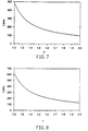
- Figure 7 is a graph illustrating the relationship between film thickness (t) and index of refraction (n) of an AES photoblank of the invention to achieve the target transmission and phase shift from at a lithographic wavelength of 193 nm.
- Figure 8 is a graph illustrating the relationship between film thickness (t) and index of refraction (n) of an AES photoblank of the invention to achieve the target transmission and phase shift from at a lithographic wavelength of 248 nm.
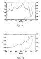
- Figure 9 is a graph showing the index of refraction "n” (solid line) and extinction coefficient "k” (broken line) of TEFLON® AF2130 / 4-perfluorooctylphenyl(trimethoxy) silane as a function of energy (E).
- Figure 10 is a graph showing the index of refraction "n" (solid line) and extinction coefficient "k” (broken line) of TEFLON® AF2130 / 4-perfluorooctylphenyl(trimethoxy) silane polysilicate interpenetrating polymers as a function of energy (E).
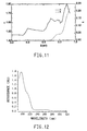
- Figure 11 is a graph illustrating the index of refraction "n" (solid line) and extinction coefficient "k” (broken line) of 5% phenylsilicate as a function of energy (E).
- Figure 12 is a UV absorption spectrum of a 1000 ⁇ phenylsilicate film before and after reactive ion etching.
- Figure 13 is a graph illustrating the spectral transmission (%T) as a function of % phenanthryl in AES photoblanks of this invention comprising phenanthrylsilicate polymer films at lithographic wavelengths of 193 nm and 248 nm.
- Figure 14 is a graph illustrating the index of refraction "n"(solid line) and extinction coefficient "k” (broken line) of phenanthrylphenylsilicate as a function of energy (E).
- Suitable AES photoblanks of this invention will have transmissions (at the selected lithographic wavelength below 400 nm) in the range from 0.005 transmission to 0.25 transmission (on an absolute transmission basis).
- the preferred transmission range is from 0.02 to 0.14 transmission at a selected lithographic wavelength below 400 nm.
- phase shift means a phase shift of 180° ⁇ 10° or odd multiples thereof.
- a particular advantage of this invention lies in enabling the production of optically tunable polymeric materials which have the correct optical constants to balance the attenuation of the material, represented by the materials extinction coefficient, and the phase shifting ability of the material represented by its index of refraction.
- the first step in practicing this invention involves demonstrating the optical performance of transmissive attenuating embedded phase shifter photoblanks for use at wavelengths below 400 nm, such as for example, 193 nm (approximately 6.45 eV) and 248 nm (approximately 5 eV), so as to define the polymeric materials target optical constants.
- This will produce a series of figures where the transmissive attenuating embedded phase shifter photoblank materials design criteria will be given. These will define, for a given index of refraction at the lithographic wavelength, what the polymeric material's extinction coefficient and the AES photoblanks film thickness must be. These AES photoblank designs and design criteria can then be developed.
- optical properties index of refraction, "n” and extinction coefficient, "k" are determined from variable angle spectroscopic ellipsometry at three incident angles from 186-800 nm, corresponding to an energy range of 1.5-6.65 eV, in combination with optical reflection and transmission data.
- Optical constants were fit to these data simultaneously, using an optical model of the film that allowed for less dense (50%) interfacial layers at the substrate and the top surface of the film. From knowledge of the spectral dependence of optical properties, the film thickness corresponding to 180° phase shift, optical transmissivity, and reflectivity can be calculated. See generally, O. S. Heavens, Optical Properties of Thin Solid Films, pp. 55-62, Dover, NY, 1991, incorporated herein by reference.
- phenanthrylsilicate (discussed in greater detail in Example 4 below) designed as a AES photoblank for use at in one case a lithographic wavelength of 193 nm and in the other case a lithographic wavelength of 248 nm.
- an AES photoblank for use at a 193 nm lithographic wavelength can be designed with a film thickness of 174.5 nm.
- This same polymeric material can be used to produce an AES photoblank for use at 248 nm by using a AES film thickness of 221.5 nm and it will have a transmission of 0.031 (shown in Figure 4) and a phase shift of 180° (shown in Figure 5) at the 243 nm lithographic wavelength.
- transmissive attenuated embedded phase shifter photomask blank having an absolute transmission in the range from 0.005 to 0.25 transmission or in the preferred transmission range of 0.02 to 0.14 transmission at the selected lithographic wavelength below 400 nm.
- the values of the index of refraction (n) and the ext-inction coefficient (k) are shown for attenuating embedded phase shifter photoblanks for various transmission levels. Within these ranges, a relationship between the polymers index of refraction at the selected lithographic wavelength and the necessary extinction coefficient of the polymer to achieve a desired AES photoblank transmission.
- the necessary thickness of the AES photoblank film can be calculated for the selected lithographic wavelength.
- the AES photoblank film thickness will vary with the selected lithographic wavelength, as shown in Figure 7 for a selected lithographic wavelength of 193 nm and in Figure 8 for a selected lithographic wavelength of 248 nm.
- the polymeric materials suitable for use in the present invention are distinguished functionally from the more common solid state inorganic shifters such as the chromium oxide/nitride family.
- optical behavior in the polymeric materials general arises from isolated molecular chromophores rather than the extended solid state bands in typical inorganic materials. Therefore, absorption in polymeric materials show rather narrow wavelength-dependent maxima rather than broad extensive absorption edges seen in typical inorganic materials. Because of the narrowness of these molecular absorption, a single chromophore is likely to exhibit very different values of the extinction coefficient at both 193 and 248 nm.
- the useful polymeric materials are amorphous fluoropolymers containing a chromophore and organically modified silicates, also known as organosilicates containing an aromatic group. It is particularly desirable that the amorphous fluoropolymers and/or organosilicates chosen be soluble in liquid and suitable for spin coating. Uniform films in the desired thickness range of about 100-400 nm can be generated rapidly and with substantially less capital investment by spin-coating than by vapor deposition.
- One class of polymeric materials useful in the practice of this invention are amorphous fluoropolymers having an index of refraction (at the selected lithographic wavelength) in a range from 1.2 to 2.0, preferably in the range from 1.26 to 1.8 and an extinction coefficient (at the selected lithographic wavelength) in a range from 0.04 to 0.8 , preferably in the range from 0.06 to 0.59.
- the amorphous fluoropolymer should contain a chromophore, such as fluorine functionalized organosilane.
- Specific amorphous fluoropolymers which can meet these criteria include terpolymers of tetrafluoroethylene. dioxole and chlorotrifluoroethylene.
- Such polymeric materials are commercially available and are commonly characterized by low dielectric constants and high resistance to a wide variety of chemical reagents.
- the prototypical fluoropolymer is polytetrafluoroethylene, sold by the DuPont Company under the trademark TEFLON® . It is a highly crystalline material with no known solvents. In the late 1980's a new class of soluble fluoropolymers was developed. For example. TEFLON® AF2130, a co-polymer of tetrafluoroethylene and perfluoro(2,3-dimethyl-1,3-dioxole) is amorphous and soluble in a variety of completely fluorinated solvents. See e.g., P. R.
- TEFLON® AF One of the remarkable characteristics of TEFLON® AF is its extraordinary transparency in the visible and UV. Although far too transparent for AES (by a factor of 500) as a pure material, TEFLON® AF could be used as a transparent matrix into which a suitable chromophore could be added. Such a material combination could exist as isolated molecules in a continuous fluoropolymer phase or, preferable as an interpenetrating system in which the chromophore itself is a polymeric material which also forms a continuous phase. Interpenetrating polymers (IPNs), in which each phase threads through the other, are well known in polymer science. See e.g. , "Interpenetrating Polymer Networks", American Chem. Soc.
- An IPN would have the potential advantages of improving the normally poor adhesion of the fluoropolymer to silica and of lessening the tendency of gross phase separation of the chromophore from the fluoropolymer. Phase separation in the AES would likely give rise to an unacceptable amount of light scattering.
- organosilicates having an index of refraction (at the selected lithographic wavelength) in a range from 1.2 to 2.0, preferably in the range from 1.26 to 1.8 and an extinction coefficient (at the selected lithographic wavelength) in a range from 0.04 to 0.8 , preferably in the range from 0.06 to 0.59. These organosilicates can be used alone or in combination with the amorphous fluoropolymers discussed above.
- silane precursors for glassy coatings are well known from the spin-on-glass and sol-gel types of materials.
- the silanes may contain four alkoxy groups which are removed by hydrolysis, leaving Si-OH groups available for network formation. Alternatively, they may contain three such alkoxy groups and one permanent (directly attached) organic group. Idealized chemical reactions for the two cases are shown below.
- the condensed network product for the organic silicate path with empirical formula R'SiO 1.5 is also known as a silsesquioxane. These are often soluble materials and can be spin coated to give transparent films. They have excellent thermal stability and adhesion to silica. Organosilicate materials and their preparation have been recently reviewed by R. Baney, M. Itoh, A. Sakakibara and T. Suzuki. Chem. Rev . 95, 1409 (1995).
- Suitable organosilicates contain aromatic groups (i.e., derived from benzene and phenanthrene) and have very strong UV absorption. Since these chromophores have higher than desired extinction coefficients, they must be diluted by either the purely inorganic silicates (e.g., from Si(OCH 3 ) 4 ) or by other organic silicates in which the R' group is non- or weakly absorbing at the selected lithographic wavelength. Methyl and other simple saturated alkyl groups are suitably non-absorbing.
- An optically suitable organosilicate diluent molecule would then be CH 3 Si(OCH 3 ) 3 Despite the strong absorption of the phenyl (C 6 H 5 ) group at 193, it is too weakly absorbing at 248 nm to be of use in an AES photoblank. However. an organosilicate based on the aromatic system phenanthrene absorbs strongly at both 193 and 248 nm.
- chromophores With respect to chromophores, it is well known that simple aromatic molecules such as benzene, or more complex aromatic molecules containing several aromatic rings linked or fused together, such as naphthalene, anthracene or phenanthrene, are all strong absorbers of ultraviolet radiation. These types of structures generally retain their optical properties when incorporated into other molecular systems such as aromatic silicates, which are useful in the practice of this invention. It is also possible to modify optical properties to some extent with certain functional groups such as nitro. especially when such groups are strongly electron donating or withdrawing or are conjugated with the aromatic ring. The effect of linking together several rings, as in phenanthrene, is to extend the UV absorption to longer wavelengths. With AES materials, the very strong absorption of benzene, i.e., the phenyl group, at 193 nm can be extended to 248 nm in phenanthrene.
- TEFLON® AF2130 An amorphous fluoropolymer, TEFLON® AF2130, was synthesized by free radical co-polymerization of chlorotrifluoroethylene and perfluoro(2,3-dimethyl) 1,3-dioxole in the approximate weight ratios of 85/15.
- the TEFLON® AF2130 polymer was dissolved in a fluorocarbon liquid solvent to give a 6.1% by wt. solution. 100 mg pure FAPS (synthesized as described in U. S. Patent 5,180,845) was then added to the fluoropolymer solution with stirring. The combined solution was then used to spin coat a film on a fused silica substrate at a spin rate of 2000 rpm, with a duration of two minutes. The film was then dried in air for 10 minutes at 100 °C to evaporate residual solvent. The film thickness was determined to be 986 nm by ellipsometry.
- this FAPS/ TEFLON® AF2130 polymer has optical constants which fall into the preferred range to produce AES photoblanks for use at 193 nm.
- Table 2 the values of the optical constants of the FAPS/TEFLON® AF2130 polymer are compared to the optical constants of a TEFLON® AF2130 polymer and it is seen that TEFLON® AF2130 does not fall into the range or the preferred range of optical constants to produce AES photoblanks for use at either 248 nm or 193 nm.
- the relative ratios of FAPS to TEFLON® AF2130 can be varied to tune the optical constants in the AES photoblanks ranges so as to produce AES photoblanks with varying transmissions and 180° phase shift.
- a fused silica slide was spin coated at the speed of 1000 rpm for two minutes with a solution of 1.7% FAPS polysilicate and 2.9% TEFLON® AF2130 in FC-40 (a fluorocarbon solvent sold by 3M). The film was heated in air to 280°C for 30 minutes to remove the solvent and densify the polysilicate network. The thickness of the coating was determined by surface profilometry to be 102 nm.
- the FAPS polysilicate was prepared by dissolving 109 mg of FAPS in 650 gm trifluoroethanol (FEH). Then 100 mg of a 10% by weight solution of de-ionized water in FEH was added. An opaque suspension resulted. 695 mg FC-40 was then added and the suspension vigorously shaken.
- this FAPS polysilicate/TEFLON® AF2130 polymer has optical constants which fall into the preferred range to produce AES photoblanks for use at 193 nm.
- Table 3 the values of the optical constants of this FAPS polysilicate/ TEFLON® AF2130 combination are compared to the optical constants of a TEFLON® AF2130 polymer.
- the relative ratios of FAPS polysilicate to TEFLON® AF2130 can be varied to tune the optical constants in the AES photoblanks ranges so as to produce AES photoblanks with varying transmissions and 180° phase shift.
- organosilicates can be used to produce AES photoblanks.
- this 5% phenyl silicate polymer has optical constants which fall into the preferred range to produce AES photoblanks for use at 193 nm.
- Table 4 the values of the optical constants for 100% phenyl silicate polymer and 5% phenyl silicate polymer are compared to the optical constants of a pure silica. It is seen from that data that pure silica does not fall into the range of optical constants to produce AES photoblanks for use at either 248 nm or 193 nm.
- pure phenyl silicate is too strongly absorbing and also does not fall into the acceptable range.
- the phenyl content of the organosilicate can be varied to tune the optical constants in the AES photoblanks ranges so as to produce AES photoblanks with varying transmissions and 180° phase shift.
- RIE reactive ion etched
- Example 4 The compound PhenanSi was synthesized from the reaction of magnesium with 9-bromophenanthrene followed by reaction of the resultant phenanthryl magnesium bromide with tetramethoxysilane as follows.
- the relative concentration of phenanthryl silicate can be varied to tune the optical constants in the AES photoblanks ranges so as to produce AES photoblanks with varying transmissions and 180° phase shift.
- the AES photoblank transmissions is shown in Figure 13 for a series of polymers with varying phenanthryl concentration.
- Optical properties of the resulting film were then determined.
- the absorption of phenyl containing polymers is much stronger at 193 nm than at 248 nm, while phenanthryl is a good absorber at both 248 and 193 nm. Therefore it becomes possible, using the flexibility inherent in the chemistry of these polymeric materials, to produce a phenanthryl phenyl silicate for which one polymeric material can be used to produce AES photoblanks with the same transmission at different lithographic wavelengths.
- This polymer has the advantage that one composition can be used to produce a family of embedded shifters for multiple lithographic wavelengths where only the AES photoblank film thickness need to be varied for application at each lithographic wavelength.
- compositional tuning of phenanthryl phenyl silicates allowed the AES photoblank designer the ability to independently tune the optical constants at for examples 248 nm and 193 nm so as to arrive at identical values of n+ik at each wavelength. Then only the AES photoblank film thickness is required to determine the selected lithographic wavelength. This can be seen from the spectral optical constants in Figure 14 of the 8% phenanthryl 3% phenyl silicate polymer. Table 6, reports the optical constants of this 8% phenanthryl 3% phenyl silicate polymer and, for comparison, the optical constants of 8% phenanthryl silicate, where the optical constants at 193 nm and 248 nm are different.
- the relative concentration of phenanthryl and phenyl in the silicate can be varied to tune the optical constants in the AES photoblanks ranges so as to produce AES photoblanks with varying transmissions and 180° phase shift while still producing comparable optical properties and AES photoblank transmissions at both 193 nm and 248 nm lithographic wavelengths.
- Optical Constants Material n + ik (193 nm) n + ik (248 nm) 8 % Phenanthryl 3 % Phenylsilicate 1.705 + i 0.171 1.687 + i 0.175 8 % Phenanthrylsilicate 1.611 + i 0.124 1.604 + i 0.229
Landscapes
- Physics & Mathematics (AREA)
- General Physics & Mathematics (AREA)
- Silicon Polymers (AREA)
- Preparing Plates And Mask In Photomechanical Process (AREA)
- Electron Beam Exposure (AREA)
- Exposure And Positioning Against Photoresist Photosensitive Materials (AREA)
- Addition Polymer Or Copolymer, Post-Treatments, Or Chemical Modifications (AREA)
- Packages (AREA)
- Compositions Of Macromolecular Compounds (AREA)
Claims (10)
- Polymer-Rohling für eine lichtdurchlässige, lichtschwächende, eingebettete Phasenschieber-Photomaske mit mindestens einem Polymerwerkstoff, der aufweist:wobei der Polymerwerkstoff unter den folgenden Materialien ausgewählt wird:(a) einen Brechungsindex (n) im Bereich von 1,2 bis 2,0 bei einer ausgewählten lithographischen Wellenlänge unter 400 nm; und(b) einen Exfinktionskoeffizienten (k) im Bereich von 0,04 bis 0,8 bei der ausgewählten lithographischen Wellenlänge unter 400 nm;vorausgesetzt, daß die gewählte Wellenlänge 193 nm beträgt, wenn die in dem Organosilicat enthaltene aromatische Gruppe Phenyl ist.(i) einem amorphen Fluorpolymer, das einen Chromophor enthält;(ii) Organosilicaten, die eine aromatische Gruppe enthalten, wobei das Organosilicat durch anorganische Silicate, organische Silicate oder ein Gemisch daraus verdünnt ist; .(iii) und Gemischen daraus;
- Photomaskenrohling nach Anspruch 1, wobei der Brechungsindex bei der ausgewählten lithographischen Wellenlänge im Bereich von 1,26 bis 1,8 liegt.
- Photomaskenrohling nach Anspruch 1 oder Anspruch 2, wobei der Extinktionskoeffizient bei der gewählten lithographischen Wellenlänge im Bereich von 0,06 bis 0,59 liegt.
- Photomaskenrohling nach einem der vorstehenden Ansprüche, wobei der in dem Fluorpolymer enthaltene Chromophor ein fluorfunktionalisiertes Organosilan ist.
- Photomaskenrohling nach einem der vorstehenden Ansprüche, wobei das Fluorpolymer TEFLON® AF2130 ist.
- Photomaskenrohling nach Anspruch 5, wobei das fluorfunktionalisierte Organosilan ein Fluoralkylphenylsilan ist.
- Photomaskenrohling nach Anspruch 5, wobei das fluorfunktionalisierte Organosilan 4-Perfluoroctylphenyl(trimethoxy)silan ist.
- Photomaskenrohling nach einem der vorstehenden Ansprüche, wobei die in dem Organosilicat enthaltene aromatische Gruppe unter Phenanthryl, Naphthyl, Anthryl, Phenyl und deren Gemischen ausgewählt ist.
- Photomaskenrohling nach einem der vorstehenden Ansprüche, wobei die in dem Organosilicat enthaltene aromatische Gruppe ein Gemisch aus Phenyl und Phenanthryl ist.
- Photomaskenrohling nach einem der vorstehenden Ansprüche, wobei die in dem Organosilicat enthaltene aromatische Gruppe Phenanthryl ist.
Applications Claiming Priority (5)
| Application Number | Priority Date | Filing Date | Title |
|---|---|---|---|
| US2146096P | 1996-07-03 | 1996-07-03 | |
| US21460P | 1996-07-03 | ||
| US79744497A | 1997-02-10 | 1997-02-10 | |
| US797444 | 1997-02-10 | ||
| PCT/US1997/011523 WO1998000758A1 (en) | 1996-07-03 | 1997-06-30 | Photomask blanks |
Publications (2)
| Publication Number | Publication Date |
|---|---|
| EP0909406A1 EP0909406A1 (de) | 1999-04-21 |
| EP0909406B1 true EP0909406B1 (de) | 2001-11-21 |
Family
ID=26694721
Family Applications (1)
| Application Number | Title | Priority Date | Filing Date |
|---|---|---|---|
| EP97933253A Expired - Lifetime EP0909406B1 (de) | 1996-07-03 | 1997-06-30 | Rohling für belichtungsmaske |
Country Status (11)
| Country | Link |
|---|---|
| US (1) | US6096460A (de) |
| EP (1) | EP0909406B1 (de) |
| JP (1) | JP2000514205A (de) |
| CN (1) | CN1124519C (de) |
| AT (1) | ATE209368T1 (de) |
| DE (1) | DE69709738T2 (de) |
| DK (1) | DK0909406T3 (de) |
| ES (1) | ES2165618T3 (de) |
| PT (1) | PT909406E (de) |
| TW (1) | TW354392B (de) |
| WO (1) | WO1998000758A1 (de) |
Families Citing this family (22)
| Publication number | Priority date | Publication date | Assignee | Title |
|---|---|---|---|---|
| AU5600200A (en) * | 1999-06-10 | 2001-01-02 | Allied-Signal Inc. | Spin-on-glass anti-reflective coatings for photolithography |
| US6824879B2 (en) * | 1999-06-10 | 2004-11-30 | Honeywell International Inc. | Spin-on-glass anti-reflective coatings for photolithography |
| US6268457B1 (en) * | 1999-06-10 | 2001-07-31 | Allied Signal, Inc. | Spin-on glass anti-reflective coatings for photolithography |
| JP3932805B2 (ja) * | 2000-12-25 | 2007-06-20 | 株式会社日立製作所 | フォトマスク及びそれを用いた電子デバイスの製造方法 |
| US6958123B2 (en) * | 2001-06-15 | 2005-10-25 | Reflectivity, Inc | Method for removing a sacrificial material with a compressed fluid |
| EP1478682A4 (de) * | 2001-11-15 | 2005-06-15 | Honeywell Int Inc | Antireflexionsbeschichtungen für die photolithographie und herstellungsverfahren dafür |
| DE10227807A1 (de) * | 2002-06-21 | 2004-01-22 | Honeywell Specialty Chemicals Seelze Gmbh | Silylalkylester von Anthracen- und Phenanthrencarbonsäuren |
| US6855463B2 (en) * | 2002-08-27 | 2005-02-15 | Photronics, Inc. | Photomask having an intermediate inspection film layer |
| US7022436B2 (en) | 2003-01-14 | 2006-04-04 | Asml Netherlands B.V. | Embedded etch stop for phase shift masks and planar phase shift masks to reduce topography induced and wave guide effects |
| JP4223840B2 (ja) * | 2003-03-12 | 2009-02-12 | 住友化学株式会社 | フォトマスク及び拡散反射板 |
| US8053159B2 (en) | 2003-11-18 | 2011-11-08 | Honeywell International Inc. | Antireflective coatings for via fill and photolithography applications and methods of preparation thereof |
| TW200641517A (en) * | 2005-05-19 | 2006-12-01 | Promos Technologies Inc | Levenson phase shifting mask and method for preparing the same and method for preparing a semiconductor device using the same |
| TWI269937B (en) * | 2005-10-13 | 2007-01-01 | Promos Technologies Inc | Phase shifting mask and method for preparing the same and method for preparing a semiconductor device using the same |
| TWI314245B (en) * | 2006-04-28 | 2009-09-01 | Promos Technologies Inc | Phase shifting mask capable of reducing the optical proximity effect and method for preparing a semiconductor device using the same |
| JP2009540084A (ja) * | 2006-06-13 | 2009-11-19 | ブラゴーン オサケ ユキチュア | 反射防止被膜用の無機−有機混成重合体組成物 |
| US8642246B2 (en) | 2007-02-26 | 2014-02-04 | Honeywell International Inc. | Compositions, coatings and films for tri-layer patterning applications and methods of preparation thereof |
| JP2009175747A (ja) * | 2009-03-24 | 2009-08-06 | Honeywell Internatl Inc | フォトリソグラフィー用スピンオン反射防止膜 |
| US8557877B2 (en) | 2009-06-10 | 2013-10-15 | Honeywell International Inc. | Anti-reflective coatings for optically transparent substrates |
| US8864898B2 (en) | 2011-05-31 | 2014-10-21 | Honeywell International Inc. | Coating formulations for optical elements |
| JP2011221549A (ja) * | 2011-06-09 | 2011-11-04 | Honeywell Internatl Inc | フォトリソグラフィー用スピンオン反射防止膜 |
| JP6420958B2 (ja) * | 2014-03-04 | 2018-11-07 | Hoya株式会社 | インプリント用モールドブランクおよびインプリント用モールド |
| EP3194502A4 (de) | 2015-04-13 | 2018-05-16 | Honeywell International Inc. | Polysiloxanformulierungen und beschichtungen für optoelektronische anwendungen |
Family Cites Families (6)
| Publication number | Priority date | Publication date | Assignee | Title |
|---|---|---|---|---|
| US4890309A (en) * | 1987-02-25 | 1989-12-26 | Massachusetts Institute Of Technology | Lithography mask with a π-phase shifting attenuator |
| US5100503A (en) * | 1990-09-14 | 1992-03-31 | Ncr Corporation | Silica-based anti-reflective planarizing layer |
| US5354632A (en) * | 1992-04-15 | 1994-10-11 | Intel Corporation | Lithography using a phase-shifting reticle with reduced transmittance |
| TW505829B (en) * | 1992-11-16 | 2002-10-11 | Dupont Photomasks Inc | A transmissive embedded phase shifter-photomask blank |
| US5415953A (en) * | 1994-02-14 | 1995-05-16 | E. I. Du Pont De Nemours And Company | Photomask blanks comprising transmissive embedded phase shifter |
| US5726247A (en) * | 1996-06-14 | 1998-03-10 | E. I. Du Pont De Nemours And Company | Fluoropolymer nanocomposites |
-
1997
- 1997-06-16 TW TW086108319A patent/TW354392B/zh active
- 1997-06-30 JP JP50444298A patent/JP2000514205A/ja not_active Ceased
- 1997-06-30 DK DK97933253T patent/DK0909406T3/da active
- 1997-06-30 DE DE69709738T patent/DE69709738T2/de not_active Expired - Fee Related
- 1997-06-30 AT AT97933253T patent/ATE209368T1/de not_active IP Right Cessation
- 1997-06-30 ES ES97933253T patent/ES2165618T3/es not_active Expired - Lifetime
- 1997-06-30 PT PT97933253T patent/PT909406E/pt unknown
- 1997-06-30 WO PCT/US1997/011523 patent/WO1998000758A1/en not_active Ceased
- 1997-06-30 EP EP97933253A patent/EP0909406B1/de not_active Expired - Lifetime
- 1997-06-30 CN CN97196087A patent/CN1124519C/zh not_active Expired - Fee Related
-
1999
- 1999-04-20 US US09/294,575 patent/US6096460A/en not_active Expired - Fee Related
Also Published As
| Publication number | Publication date |
|---|---|
| ATE209368T1 (de) | 2001-12-15 |
| US6096460A (en) | 2000-08-01 |
| WO1998000758A1 (en) | 1998-01-08 |
| DK0909406T3 (da) | 2002-05-21 |
| CN1224513A (zh) | 1999-07-28 |
| EP0909406A1 (de) | 1999-04-21 |
| ES2165618T3 (es) | 2002-03-16 |
| DE69709738D1 (de) | 2002-02-21 |
| TW354392B (en) | 1999-03-11 |
| DE69709738T2 (de) | 2002-08-08 |
| JP2000514205A (ja) | 2000-10-24 |
| PT909406E (pt) | 2002-03-28 |
| CN1124519C (zh) | 2003-10-15 |
Similar Documents
| Publication | Publication Date | Title |
|---|---|---|
| EP0909406B1 (de) | Rohling für belichtungsmaske | |
| US6174631B1 (en) | Attenuating phase shift photomasks | |
| US5538816A (en) | Halftone phase shift photomask, halftone phase shift photomask blank, and methods of producing the same | |
| KR100362126B1 (ko) | 포토마스크블랭크 | |
| Bloomstein et al. | Lithography with 157 nm lasers | |
| US6514667B2 (en) | Tunable vapor deposited materials as antireflective coatings, hardmasks and as combined antireflective coating/hardmasks and methods of fabrication thereof and applications thereof | |
| US6835503B2 (en) | Use of a planarizing layer to improve multilayer performance in extreme ultra-violet masks | |
| JP3938940B2 (ja) | 移相フォトマスク・ブランク及びそれを製造する方法 | |
| JP3115185B2 (ja) | 露光用マスクとパターン形成方法 | |
| US7622227B2 (en) | Phase-shift photomask-blank, phase-shift photomask and fabrication method thereof | |
| US6319639B1 (en) | Method for making a photomask with multiple absorption levels | |
| US6395433B1 (en) | Photomask for projection lithography at or below about 160 nm and a method thereof | |
| TWI767369B (zh) | 半色調衰減式相移空白遮罩以及用於極紫外光微影的光罩 | |
| US20110244378A1 (en) | Device and method for providing wavelength reduction with a photomask | |
| EP1286217B1 (de) | Rohling für Phasenschiebermaske, deren Herstellung und Gebrauch | |
| CN1646994B (zh) | 嵌入式衰减相移光掩模坯料 | |
| US8709683B2 (en) | Photomask blank, photomask blank manufacturing method, and photomask manufacturing method | |
| JP3301215B2 (ja) | ハーフトーン型位相シフトマスク、ハーフトーン型位相シフトマスクの作製に用いる半透明部形成材料、及びハーフトーン型位相シフトマスクの作製方法 | |
| KR100495290B1 (ko) | 포토마스크블랭크 | |
| US6682860B2 (en) | Attenuated embedded phase shift photomask blanks | |
| JP6700120B2 (ja) | フォトマスクブランクおよびフォトマスク、製造方法 | |
| JP2002189283A (ja) | 位相シフトマスクブランク、位相シフトマスク及び位相シフトマスクの製造方法 | |
| Kim et al. | Silicon-based anti-reflective spin-on hardmask materials with improved storage stability for 193-nm lithography | |
| JPH04307545A (ja) | 位相シフトマスクおよびその製造方法 | |
| KR0154017B1 (ko) | 미세 패턴 형성 방법 |
Legal Events
| Date | Code | Title | Description |
|---|---|---|---|
| PUAI | Public reference made under article 153(3) epc to a published international application that has entered the european phase |
Free format text: ORIGINAL CODE: 0009012 |
|
| 17P | Request for examination filed |
Effective date: 19981218 |
|
| AK | Designated contracting states |
Kind code of ref document: A1 Designated state(s): AT BE CH DE DK ES FR GB GR IE IT LI LU NL PT SE |
|
| 17Q | First examination report despatched |
Effective date: 19991214 |
|
| GRAG | Despatch of communication of intention to grant |
Free format text: ORIGINAL CODE: EPIDOS AGRA |
|
| GRAG | Despatch of communication of intention to grant |
Free format text: ORIGINAL CODE: EPIDOS AGRA |
|
| GRAH | Despatch of communication of intention to grant a patent |
Free format text: ORIGINAL CODE: EPIDOS IGRA |
|
| GRAH | Despatch of communication of intention to grant a patent |
Free format text: ORIGINAL CODE: EPIDOS IGRA |
|
| GRAA | (expected) grant |
Free format text: ORIGINAL CODE: 0009210 |
|
| AK | Designated contracting states |
Kind code of ref document: B1 Designated state(s): AT BE CH DE DK ES FR GB GR IE IT LI LU NL PT SE |
|
| PG25 | Lapsed in a contracting state [announced via postgrant information from national office to epo] |
Ref country code: GR Free format text: LAPSE BECAUSE OF FAILURE TO SUBMIT A TRANSLATION OF THE DESCRIPTION OR TO PAY THE FEE WITHIN THE PRESCRIBED TIME-LIMIT Effective date: 20011121 |
|
| REF | Corresponds to: |
Ref document number: 209368 Country of ref document: AT Date of ref document: 20011215 Kind code of ref document: T |
|
| REG | Reference to a national code |
Ref country code: CH Ref legal event code: EP |
|
| REG | Reference to a national code |
Ref country code: IE Ref legal event code: FG4D |
|
| REG | Reference to a national code |
Ref country code: GB Ref legal event code: IF02 |
|
| REG | Reference to a national code |
Ref country code: CH Ref legal event code: NV Representative=s name: RITSCHER & PARTNER AG PATENTANWAELTE |
|
| REF | Corresponds to: |
Ref document number: 69709738 Country of ref document: DE Date of ref document: 20020221 |
|
| REG | Reference to a national code |
Ref country code: ES Ref legal event code: FG2A Ref document number: 2165618 Country of ref document: ES Kind code of ref document: T3 |
|
| REG | Reference to a national code |
Ref country code: PT Ref legal event code: SC4A Free format text: AVAILABILITY OF NATIONAL TRANSLATION Effective date: 20011212 |
|
| ET | Fr: translation filed | ||
| REG | Reference to a national code |
Ref country code: DK Ref legal event code: T3 |
|
| REG | Reference to a national code |
Ref country code: GR Ref legal event code: EP Ref document number: 20010402456 Country of ref document: GR |
|
| PGFP | Annual fee paid to national office [announced via postgrant information from national office to epo] |
Ref country code: SE Payment date: 20020611 Year of fee payment: 6 |
|
| PGFP | Annual fee paid to national office [announced via postgrant information from national office to epo] |
Ref country code: AT Payment date: 20020612 Year of fee payment: 6 |
|
| PGFP | Annual fee paid to national office [announced via postgrant information from national office to epo] |
Ref country code: DK Payment date: 20020614 Year of fee payment: 6 |
|
| PGFP | Annual fee paid to national office [announced via postgrant information from national office to epo] |
Ref country code: ES Payment date: 20020618 Year of fee payment: 6 |
|
| PGFP | Annual fee paid to national office [announced via postgrant information from national office to epo] |
Ref country code: PT Payment date: 20020620 Year of fee payment: 6 |
|
| PGFP | Annual fee paid to national office [announced via postgrant information from national office to epo] |
Ref country code: IE Payment date: 20020625 Year of fee payment: 6 |
|
| PGFP | Annual fee paid to national office [announced via postgrant information from national office to epo] |
Ref country code: GR Payment date: 20020626 Year of fee payment: 6 |
|
| PGFP | Annual fee paid to national office [announced via postgrant information from national office to epo] |
Ref country code: NL Payment date: 20020628 Year of fee payment: 6 |
|
| PGFP | Annual fee paid to national office [announced via postgrant information from national office to epo] |
Ref country code: DE Payment date: 20020702 Year of fee payment: 6 Ref country code: CH Payment date: 20020702 Year of fee payment: 6 |
|
| PGFP | Annual fee paid to national office [announced via postgrant information from national office to epo] |
Ref country code: LU Payment date: 20020708 Year of fee payment: 6 |
|
| PGFP | Annual fee paid to national office [announced via postgrant information from national office to epo] |
Ref country code: BE Payment date: 20020830 Year of fee payment: 6 |
|
| PLBE | No opposition filed within time limit |
Free format text: ORIGINAL CODE: 0009261 |
|
| STAA | Information on the status of an ep patent application or granted ep patent |
Free format text: STATUS: NO OPPOSITION FILED WITHIN TIME LIMIT |
|
| 26N | No opposition filed | ||
| PG25 | Lapsed in a contracting state [announced via postgrant information from national office to epo] |
Ref country code: LU Free format text: LAPSE BECAUSE OF NON-PAYMENT OF DUE FEES Effective date: 20030630 Ref country code: LI Free format text: LAPSE BECAUSE OF NON-PAYMENT OF DUE FEES Effective date: 20030630 Ref country code: IE Free format text: LAPSE BECAUSE OF NON-PAYMENT OF DUE FEES Effective date: 20030630 Ref country code: DK Free format text: LAPSE BECAUSE OF NON-PAYMENT OF DUE FEES Effective date: 20030630 Ref country code: CH Free format text: LAPSE BECAUSE OF NON-PAYMENT OF DUE FEES Effective date: 20030630 Ref country code: BE Free format text: LAPSE BECAUSE OF NON-PAYMENT OF DUE FEES Effective date: 20030630 Ref country code: AT Free format text: LAPSE BECAUSE OF NON-PAYMENT OF DUE FEES Effective date: 20030630 |
|
| PG25 | Lapsed in a contracting state [announced via postgrant information from national office to epo] |
Ref country code: SE Free format text: LAPSE BECAUSE OF NON-PAYMENT OF DUE FEES Effective date: 20030701 Ref country code: ES Free format text: LAPSE BECAUSE OF NON-PAYMENT OF DUE FEES Effective date: 20030701 |
|
| BERE | Be: lapsed |
Owner name: E.I. *DU PONT DE NEMOURS AND CY Effective date: 20030630 |
|
| PG25 | Lapsed in a contracting state [announced via postgrant information from national office to epo] |
Ref country code: PT Free format text: LAPSE BECAUSE OF NON-PAYMENT OF DUE FEES Effective date: 20031231 |
|
| PG25 | Lapsed in a contracting state [announced via postgrant information from national office to epo] |
Ref country code: NL Free format text: LAPSE BECAUSE OF NON-PAYMENT OF DUE FEES Effective date: 20040101 Ref country code: DE Free format text: LAPSE BECAUSE OF NON-PAYMENT OF DUE FEES Effective date: 20040101 |
|
| REG | Reference to a national code |
Ref country code: DK Ref legal event code: EBP |
|
| REG | Reference to a national code |
Ref country code: CH Ref legal event code: PL |
|
| NLV4 | Nl: lapsed or anulled due to non-payment of the annual fee |
Effective date: 20040101 |
|
| EUG | Se: european patent has lapsed | ||
| REG | Reference to a national code |
Ref country code: PT Ref legal event code: MM4A Free format text: LAPSE DUE TO NON-PAYMENT OF FEES Effective date: 20031231 |
|
| REG | Reference to a national code |
Ref country code: IE Ref legal event code: MM4A |
|
| REG | Reference to a national code |
Ref country code: ES Ref legal event code: FD2A Effective date: 20030701 |
|
| PGFP | Annual fee paid to national office [announced via postgrant information from national office to epo] |
Ref country code: FR Payment date: 20050608 Year of fee payment: 9 |
|
| PGFP | Annual fee paid to national office [announced via postgrant information from national office to epo] |
Ref country code: GB Payment date: 20050629 Year of fee payment: 9 |
|
| PG25 | Lapsed in a contracting state [announced via postgrant information from national office to epo] |
Ref country code: IT Free format text: LAPSE BECAUSE OF NON-PAYMENT OF DUE FEES;WARNING: LAPSES OF ITALIAN PATENTS WITH EFFECTIVE DATE BEFORE 2007 MAY HAVE OCCURRED AT ANY TIME BEFORE 2007. THE CORRECT EFFECTIVE DATE MAY BE DIFFERENT FROM THE ONE RECORDED. Effective date: 20050630 |
|
| PG25 | Lapsed in a contracting state [announced via postgrant information from national office to epo] |
Ref country code: GB Free format text: LAPSE BECAUSE OF NON-PAYMENT OF DUE FEES Effective date: 20060630 |
|
| GBPC | Gb: european patent ceased through non-payment of renewal fee |
Effective date: 20060630 |
|
| REG | Reference to a national code |
Ref country code: FR Ref legal event code: ST Effective date: 20070228 |
|
| PG25 | Lapsed in a contracting state [announced via postgrant information from national office to epo] |
Ref country code: FR Free format text: LAPSE BECAUSE OF NON-PAYMENT OF DUE FEES Effective date: 20060630 |