EP0908828B1 - Distributed access control system for memory and method - Google Patents
Distributed access control system for memory and method Download PDFInfo
- Publication number
- EP0908828B1 EP0908828B1 EP98402449A EP98402449A EP0908828B1 EP 0908828 B1 EP0908828 B1 EP 0908828B1 EP 98402449 A EP98402449 A EP 98402449A EP 98402449 A EP98402449 A EP 98402449A EP 0908828 B1 EP0908828 B1 EP 0908828B1
- Authority
- EP
- European Patent Office
- Prior art keywords
- memory
- entities
- entity
- allocated
- signal
- Prior art date
- Legal status (The legal status is an assumption and is not a legal conclusion. Google has not performed a legal analysis and makes no representation as to the accuracy of the status listed.)
- Expired - Lifetime
Links
Images
Classifications
-
- G—PHYSICS
- G06—COMPUTING; CALCULATING OR COUNTING
- G06F—ELECTRIC DIGITAL DATA PROCESSING
- G06F13/00—Interconnection of, or transfer of information or other signals between, memories, input/output devices or central processing units
- G06F13/14—Handling requests for interconnection or transfer
- G06F13/16—Handling requests for interconnection or transfer for access to memory bus
- G06F13/18—Handling requests for interconnection or transfer for access to memory bus based on priority control
Definitions
- the invention relates to shared access control to a random access memory by several entities that can operate completely asynchronously.
- the invention applies advantageously but not exclusively to the field of television. Indeed, in such an application, the data displayed on the TV screen is delivered by a screen controller after reading a random access memory whose content is the result of a software processing performed by a microprocessor.
- clock signals respectively clocking the screen controller and the microprocessor are totally asynchronous in frequency and phase and each of these two entities may be likely to want to access the memory at one time.
- the aim of the invention is to provide a radically different solution to access control shared to the same memory.
- the invention proposes the use of a simple random access memory, the sharing of which is not physical by different accesses. (as in dual access memories) but temporal. More specifically, time sharing of memory access requests is performed, and shared memory accesses are managed by a sequencer which will segment the time into access windows specifically reserved for each of the user entities of the memory. memory. The sequencer is punctuated by a clock chosen according to the priorities of the different entities. The internal clock signal of the highest priority entity will be the one that will rhythm the sequencer. Finally, a non-priority entity, or auxiliary, will, with each access request, wait for its next access window to read or store the data being processed.
- the invention proposes a shared access control method to a random access memory, in which a plurality of peripheral entities clocked respectively by their own internal clock signal, are able to access said memory. memory.
- the random access memory is a single access memory, that is to say a single access memory, and a priority entity is defined among the set of peripheral entities, the other entities being defined as being auxiliary entities.
- a repetitive time frame is generated, paced by the internal clock signal of the priority entity, this frame being subdivided into time windows forming several groups of windows respectively allocated to the peripheral entities. And each peripheral entity is allowed to access said memory only during the windows allocated to it.
- the priority entity will advantageously be the screen controller.
- auxiliary peripheral entities may be simple data samplers.
- Other auxiliary entities may comprise a central microprocessor unit and input / output means connected to said memory and able to contain data to be written in the memory or data extracted from the memory and to be read by the user. central unit.
- the data present in the input / output means is validated during the next time slot allocated to said central unit and the internal operation of the central unit is frozen until said validation.
- the invention also relates to an access control system shared with a random access memory.
- the system according to the invention further comprises a control interface comprising a sequencer clocked by the internal clock signal of the priority entity, so as to develop a repetitive temporal frame divided into time windows forming several groups of windows respectively allocated to peripheral entities.
- the interface also comprises control means capable of responding to an access request signal emanating from a peripheral entity, to deliver to the input / output means of this entity the data validation signal only in the course of a window allocated to this entity, thus allowing the access of this entity to the memory.
- control means advantageously comprise suitable means of inhibition, in the presence of a memory access request signal transmitted by the central unit to the central unit. during a time window that is not allocated to it, to freeze the operation internal of the central unit until the reception of the data validation signal.
- This "freezing" or this inhibition of the operation of the central unit may result in a total interruption of the operation of the central unit or in a freeze or a freezing of the contents of the internal registers or latches so that it There is no further evolution of the data delivered by these flip-flops until the gel signal is deactivated.
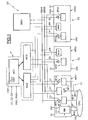
- the reference SY generally designates a system according to the invention, making it possible here to control the accesses of three peripheral entities, or more simply peripheral devices, P1, P2 and P3, to an MMV random access memory.
- peripheral P1 comprises in the example described, a microprocessor CPU central unit as well as input / output means MES1 connected to the address bus BSR1 of the memory and on the BSR2 data bus of this memory.
- these input / output means MES1 comprise an output port BF10, connected to the address bus BSR1, comprising a buffer memory, connected to the address bus BS10 of the central unit for storing an address.
- This output port BF10 is conventionally controlled by an address validation signal E1 for validating and effectively delivering the address on the address bus BSR1 of the memory.
- the input / output means MES 1 comprise a data input port BF11 comprising a buffer memory, connected between the data bus B SR2 of the memory MV and the data bus BS11 of the central unit. This input port is controlled by a signal LD1 for validating the data extracted from the memory MMV.
- the means MES 1 comprise a data output port BF12 controlled by a data validation signal D1 for actually writing the data in the memory MMV.
- MES 1 of course comprise a control port for the exchange of the different validation signals E1, LD1, D1, but also to deliver a signal C1 of access request to the memory and a signal RW1 representative of the reading direction. writing.
- the second peripheral P2 which is, for example, in a television application, the screen controller, comprises input / output means MES2 comprising a control port and an output port BF20 connected to the address bus BSR1.
- memory comprising in particular an address pointer and controllable by an address validation signal E2.
- these input / output means MES2 here comprise only a data input port BF21 comprising a buffer memory, connected to the data bus BSR2 of the memory and controllable by a data validation signal LD2.
- the system according to the invention also includes an IF interface for controlling and managing access to the MMV memory.
- this IF interface comprises processing means that can be implemented at least partially in a software manner within a microcontroller for example, or by a specific integrated circuit (ASIC), or simply by simple hardware integration (“ hardware ”) in the system (integrated circuit for example).
- ASIC application specific integrated circuit
- hardware simple hardware integration
- the IF interface has been functionally broken down.
- a main controller MC1 comprising in particular a sequencer SQ clocked by the clock signal of one of the devices so as to develop a repetitive time frame which will be discussed in more detail below on the structure, and a bus controller MC2 data delivering the data enable signals LDi and / or Di and an address bus controller MC3 delivering the address validation signals Ei.
- the development of the repetitive time frame TR depends on the priority character of one of the peripherals. More precisely, one of the peripheral entities P1, P2, P3 is selected, the one whose real-time processing is the highest priority, that is to say for example the one with the most real-time constraints.
- the priority real-time processing is that managing the display screen so as not to deteriorate the quality and stability of the displayed image. It is therefore the peripheral entity P2 corresponding to the screen controller, which will be designated as the priority entity, the other entities being the auxiliary entities.
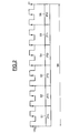
- the duration of the TR frame will be chosen here as being the time required to display a character on the screen.
- This frame duration TR corresponds to a certain number of periods of the clock signal CK2 of the screen controller. This number of clock periods is typically 18, but for simplification purposes, only 12 are shown in FIG.
- the remaining access windows namely the windows S1, S3 and S5 are reserved for the other peripheral entities.
- the CPU S1 and S5 are allocated to the CPU, while the S3 device is allocated to the peripheral entity P3.
- the sequencer of the control interface is clocked by the clock signal CK2 of the priority entity.
- requests C2 successive accesses issued by the P2 device will be synchronous with the occurrence of time windows S2, S4 and S6.
- the address validation signals E2 and LD2 will therefore be delivered by the control means MC2 and MC3 during these time slots also allowing access of the device P2 to the memory MMV.
- the control interface will deliver the address validation signal E3 and the data validation signal D3 or LD3 according to the logical value of a signal RW3, only during the next access window which is allocated to the device P3, in this case the window S3.
- the device P3 will actually have access to the memory MMV during the window S3 allocated to it.
- the same principle is applied to the device P1 in the case where an access request signal C1, associated with a write or read request signal RW1, is emitted by the device P1 during a time window of access that is not allocated to him.
- it is furthermore necessary to freeze the internal operation of the central processing unit CPU until the reception of the validation signal LD1 or D1 as a function of the reading or writing direction.
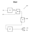
- the IF control interface comprises MH inhibiting means which is shown here for simplification purposes within the MES1 block.
- these MH inhibiting means comprise an address decoder AD receiving the address sent on the bus BS10 of the central unit and intended to verify that this address corresponds to an effective address. of memory. If this is the case, the output SEL signal of the decoder goes to logic level "1" and is stored in a flip-flop referenced BD controlled by the address validation signal ST delivered by the central unit.
- this address enable signal ST goes to 1
- the output of the flip-flop BD which is connected to the input of an FF flip flop (flip flop) passes the output of this flip-flop FF to 1.
- the signal corresponding logic WT which is delivered to the CPU CPU, then acts as a freeze signal of that unit Central. It should also be noted that the transition of the signal WT from the logical state "0" to the logic state "1" can be used as a condition for generating the access request signal C1.
- the MH inhibiting means also comprise a DT transitions detector whose output is connected to the reset input R of the FF output flip-flop, and the input of which is connected to the output of a logic gate. OR, referenced PL, and receiving as input the validation signals LD1 and D1.
- the transmission by the controller MC2 of the control interface of the data validation signal LD1 or D1 results in a rising transition of the corresponding signal.
- the detection of this transition by the detector DT has the effect of returning the output of the flip-flop FF to zero, that is to say, to redimit the WT gel signal to a low state, which has the consequence of reactivate the internal operation of the CPU.
Description
L'invention concerne le contrôle d'accès partagés à une mémoire vive par plusieurs entités pouvant fonctionner de façon complètement asynchrone.The invention relates to shared access control to a random access memory by several entities that can operate completely asynchronously.
L'invention s'applique avantageusement mais non limitativement au domaine de la télévision. En effet, dans une telle application, les données affichées sur l'écran du téléviseur sont délivrées par un contrôleur d'écran après lecture d'une mémoire vive dont le contenu est le résultat d'un traitement logiciel effectué par un microprocesseur.The invention applies advantageously but not exclusively to the field of television. Indeed, in such an application, the data displayed on the TV screen is delivered by a screen controller after reading a random access memory whose content is the result of a software processing performed by a microprocessor.
Or, les signaux d'horloge cadençant respectivement le contrôleur d'écran et le microprocesseur sont totalement asynchrones en fréquence et en phase et chacune de ces deux entités peut être susceptible de vouloir accéder à la mémoire à un même instant.However, the clock signals respectively clocking the screen controller and the microprocessor are totally asynchronous in frequency and phase and each of these two entities may be likely to want to access the memory at one time.
Une solution pour résoudre de tels accès partagés consiste à utiliser des mémoires dites "double accès", c'est-à-dire pour lesquelles deux entités sont capables aussi bien de lire ou d'écrire simultanément ou non dans chacune des cellules ou points mémoire de la mémoire. Or, une telle solution nécessite l'utilisation de mémoires de structure complexe et peut conduire à des dysfonctionnements dans certains cas spécifiques, en particulier lorsque l'une des entités souhaite écrire dans un point-mémoire alors que quasi sumultanément, l'autre entité souhaite lire ledit point-mémoire.One solution for solving such shared access is to use so-called "dual access" memories, that is to say for which two entities are able to read or write simultaneously or not simultaneously in each of the cells or memory cells. of memory. However, such a solution requires the use of complex structure memories and can lead to malfunctions in certain specific cases, particularly when one of the entities wishes to write in a memory point while almost simultaneously, the other entity wishes to read said memory point.
L'invention vise à apporter une solution radicalement différente au contrôle d'accès partagés à une même mémoire.The aim of the invention is to provide a radically different solution to access control shared to the same memory.
Ainsi, l'invention propose l'utilisation d'une mémoire vive simple accès, dont le partage n'est pas physique par différents accès (comme dans les mémoires double accès) mais temporel. Plus précisément, on effectue un partage temporel des demandes d'accès à la mémoire, et les accès partagés à la mémoire sont gérés par un séquenceur qui va segmenter le temps en fenêtres d'accès réservées de façon spécifique à chacune des entités utilisatrices de la mémoire. Le séquenceur est rythmé par une horloge choisie en fonction des priorités des différentes entités. Le signal d'horloge interne de l'entité la plus prioritaire sera celui qui rythmera le séquenceur. Enfin, une entité non prioritaire, ou auxiliaire, devra, à chacune de ses demandes d'accès, attendre que vienne sa prochaine fenêtre d'accès afin de lire ou stocker les données en cours de traitement.Thus, the invention proposes the use of a simple random access memory, the sharing of which is not physical by different accesses. (as in dual access memories) but temporal. More specifically, time sharing of memory access requests is performed, and shared memory accesses are managed by a sequencer which will segment the time into access windows specifically reserved for each of the user entities of the memory. memory. The sequencer is punctuated by a clock chosen according to the priorities of the different entities. The internal clock signal of the highest priority entity will be the one that will rhythm the sequencer. Finally, a non-priority entity, or auxiliary, will, with each access request, wait for its next access window to read or store the data being processed.
En d'autres termes, telle que revendiquée, l'invention propose un procédé de contrôle d'accès partagés à une mémoire vive, dans lequel plusieurs entités périphériques cadencées respectivement par leur propre signal d'horloge interne, sont susceptibles d'accéder à ladite mémoire.In other words, as claimed, the invention proposes a shared access control method to a random access memory, in which a plurality of peripheral entities clocked respectively by their own internal clock signal, are able to access said memory. memory.
Selon une caractéristique générale de l'invention, la mémoire vive est une mémoire simple accès, c'est-à-dire à accès unique, et on définit une entité prioritaire parmi l'ensemble des entités périphériques, les autres entités étant définies comme étant des entités auxiliaires. On élabore une trame temporelle répétitive, rythmée par le signal d'horloge interne de l'entité prioritaire, cette trame étant subdivisée en fenêtres temporelles formant plusieurs groupes de fenêtres respectivement alloués aux entités périphériques. Et on autorise chaque entité périphérique à accéder à ladite mémoire uniquement au cours des fenêtres qui lui sont allouées.According to a general characteristic of the invention, the random access memory is a single access memory, that is to say a single access memory, and a priority entity is defined among the set of peripheral entities, the other entities being defined as being auxiliary entities. A repetitive time frame is generated, paced by the internal clock signal of the priority entity, this frame being subdivided into time windows forming several groups of windows respectively allocated to the peripheral entities. And each peripheral entity is allowed to access said memory only during the windows allocated to it.
Ainsi, dans une application de télévision, l'entité prioritaire sera avantageusement le contrôleur d'écran.Thus, in a television application, the priority entity will advantageously be the screen controller.
Certaines entités périphériques auxiliaires peuvent être de simples échantillonneurs de données. D'autres entités auxiliaires peuvent comporter une unité centrale de microprocesseur et des moyens d'entrée/sortie reliés à ladite mémoire et aptes à contenir une donnée devant être écrite dans la mémoire ou une donnée extraite de la mémoire et devant être lue par l'unité centrale. Dans ce cas, selon un mode de mise en oeuvre du procédé selon l'invention, en présence d'un signal de requête d'accès à la mémoire émis par l'unité centrale au cours d'une fenêtre temporelle qui ne lui est pas allouée, on valide la donnée présente dans les moyens d'entrée/sortie au cours de la prochaine fenêtre temporelle allouée à ladite unité centrale et on gèle le fonctionnement interne de l'unité centrale jusqu'à ladite validation.Some auxiliary peripheral entities may be simple data samplers. Other auxiliary entities may comprise a central microprocessor unit and input / output means connected to said memory and able to contain data to be written in the memory or data extracted from the memory and to be read by the user. central unit. In this case, according to an embodiment of the method according to the invention, in the presence of a memory access request signal transmitted by the central unit during a window time that is not allocated to it, the data present in the input / output means is validated during the next time slot allocated to said central unit and the internal operation of the central unit is frozen until said validation.
L'invention a également pour objet un système de contrôle d'accès partagés à une mémoire vive.The invention also relates to an access control system shared with a random access memory.
Selon une caractéristique générale de l'invention, ce système comprend :
- une mémoire vive simple accès connectée sur un bus de données et un bus d'adresses,
- plusieurs entités périphériques, réparties en une entité prioritaire et en entités auxiliaires, cadencées respectivement par leur propre signal d'horloge interne. Chaque entité périphérique est apte à délivrer un signal de requête d'accès à la mémoire et comporte des moyens d'entrée/sortie, connectés sur les bus de données et d'adresses. Ces moyens d'entrée/sortie sont aptes à contenir une donnée extraite de la mémoire ou une donnée devant être écrite dans la mémoire. Ces moyens d'entrée/sortie possèdent par ailleurs un port de contrôle pour recevoir au moins un signal de validation de la donnée contenue dans les moyens d'entrée/sortie.
- a single access random access memory connected to a data bus and an address bus,
- several peripheral entities, divided into a priority entity and auxiliary entities, clocked respectively by their own internal clock signal. Each peripheral entity is capable of delivering a memory access request signal and comprises input / output means connected on the data and address buses. These input / output means are capable of containing data extracted from the memory or data to be written in the memory. These input / output means also have a control port for receiving at least one validation signal of the data contained in the input / output means.
Le système selon l'invention comprend par ailleurs une interface de contrôle comportant un séquenceur rythmé par le signal d'horloge interne de l'entité prioritaire, de façon à élaborer une trame temporelle répétitive subdivisée en fenêtres temporelles formant plusieurs groupes de fenêtres respectivement alloués aux entités périphériques. L'interface comprend également des moyens de contrôle aptes en réponse à un signal de requête d'accès émanant d'une entité périphérique, à délivrer aux moyens d'entrée/sortie de cette entité le signal de validation de données uniquement au cours d'une fenêtre allouée à cette entité, autorisant ainsi l'accès de cette entité à la mémoire.The system according to the invention further comprises a control interface comprising a sequencer clocked by the internal clock signal of the priority entity, so as to develop a repetitive temporal frame divided into time windows forming several groups of windows respectively allocated to peripheral entities. The interface also comprises control means capable of responding to an access request signal emanating from a peripheral entity, to deliver to the input / output means of this entity the data validation signal only in the course of a window allocated to this entity, thus allowing the access of this entity to the memory.
Lorsque l'une des entités auxiliaires comporte une unité centrale d'un microprocesseur, les moyens de contrôle comportent avantageusement des moyens d'inhibition aptes, en présence d'un signal de requête d'accès à la mémoire émis par l'unité centrale au cours d'une fenêtre temporelle qui ne lui est pas allouée, à geler le fonctionnement interne de l'unité centrale jusqu'à la réception du signal de validation de données.When one of the auxiliary entities comprises a central unit of a microprocessor, the control means advantageously comprise suitable means of inhibition, in the presence of a memory access request signal transmitted by the central unit to the central unit. during a time window that is not allocated to it, to freeze the operation internal of the central unit until the reception of the data validation signal.
Ce "gel" ou cette inhibition du fonctionnement de l'unité centrale peut se traduire par une interruption totale du fonctionnement de l'unité centrale ou bien par un gel ou un figeage du contenu des registres ou bascules internes de telle sorte qu'il n'y ait plus aucune évolution des données délivrées par ces bascules jusqu'à désactivation du signal de gel.This "freezing" or this inhibition of the operation of the central unit may result in a total interruption of the operation of the central unit or in a freeze or a freezing of the contents of the internal registers or latches so that it There is no further evolution of the data delivered by these flip-flops until the gel signal is deactivated.
D'autres avantages et caractéristiques de l'invention apparaîtront à l'examen de la description détaillée d'un mode de réalisation et de mise en oeuvre, nullement limitatif, et des dessins annexés, sur lesquels :
- la figure 1 est un synoptique schématique d'un système de contrôle d'accès partagés selon l'invention,
- la figure 2 illustre une trame temporelle permettant le partage temporel des accès à la mémoire, et
- la figure 3 illustre plus en détail, mais toujours de façon schématique, une partie du dispositif de la figure 1.
- FIG. 1 is a schematic block diagram of a shared access control system according to the invention,
- FIG. 2 illustrates a time frame allowing the temporal sharing of accesses to the memory, and
- FIG. 3 illustrates in more detail, but always schematically, a portion of the device of FIG.
Sur la figure 1, la référence SY désigne d'une façon générale un système selon l'invention, permettant ici de contrôler les accès de trois entités périphériques, ou plus simplement périphériques, P1, P2 et P3, à une mémoire vive MMV.In FIG. 1, the reference SY generally designates a system according to the invention, making it possible here to control the accesses of three peripheral entities, or more simply peripheral devices, P1, P2 and P3, to an MMV random access memory.
L'un de ces périphériques, en l'espèce le périphérique P1, comporte dans l'exemple décrit, une unité centrale de microprocesseur CPU ainsi que des moyens d'entrée/sortie MES1 connectés sur le bus d'adresses BSR1 de la mémoire et sur le bus de données BSR2 de cette mémoire.One of these peripherals, in this case the peripheral P1, comprises in the example described, a microprocessor CPU central unit as well as input / output means MES1 connected to the address bus BSR1 of the memory and on the BSR2 data bus of this memory.
D'une façon classique, ces moyens d'entrée/sortie MES1 comportent un port de sortie BF10, connecté sur le bus d'adresses BSR1, comportant une mémoire tampon, connectée sur le bus d'adresses BS10 de l'unité centrale pour stocker une adresse. Ce port de sortie BF10 est commandé de façon classique par un signal de validation d'adresse E1 permettant de valider et de délivrer effectivement l'adresse sur le bus d'adresses BSR1 de la mémoire.In a conventional manner, these input / output means MES1 comprise an output port BF10, connected to the address bus BSR1, comprising a buffer memory, connected to the address bus BS10 of the central unit for storing an address. This output port BF10 is conventionally controlled by an address validation signal E1 for validating and effectively delivering the address on the address bus BSR1 of the memory.
De même, les moyens d'entrée/sortie MES 1 comportent un port d'entrée de données BF11 comportant une mémoire tampon, connectée entre le bus de données B SR2 de la mémoire MV et le bus de données BS11 de l'unité centrale. Ce port d'entrée est commandé par un signal LD1 de validation de la donnée extraite de la mémoire MMV.Likewise, the input / output means MES 1 comprise a data input port BF11 comprising a buffer memory, connected between the data bus B SR2 of the memory MV and the data bus BS11 of the central unit. This input port is controlled by a signal LD1 for validating the data extracted from the memory MMV.
D'une façon analogue, pour l'écriture d'une donnée dans la mémoire MMV, les moyens MES 1 comportent un port de sortie de données BF12 commandé par un signal de validation de donnée D1 permettant d'écrire effectivement la donnée dans la mémoire MMV.In a similar way, for writing data in the memory MMV, the means MES 1 comprise a data output port BF12 controlled by a data validation signal D1 for actually writing the data in the memory MMV.
Ces moyens MES 1 comportent bien entendu un port de contrôle pour l'échange des différents signaux de validation E1, LD1, D1, mais aussi pour délivrer un signal C1 de requête d'accès à la mémoire et un signal RW1 représentatif du sens lecture/écriture.These means MES 1 of course comprise a control port for the exchange of the different validation signals E1, LD1, D1, but also to deliver a signal C1 of access request to the memory and a signal RW1 representative of the reading direction. writing.
Le deuxième périphérique P2, qui est par exemple dans une application de télévision, le contrôleur d'écran, comprend des moyens d'entrée/sortie MES2 comportant un port de contrôle et un port de sortie BF20, connecté sur le bus d'adresses BSR1 de la mémoire, comportant notamment un pointeur d'adresses et commandable par un signal de validation d'adresses E2. En outre, ces moyens d'entrée/sortie MES2 comportent ici uniquement un port d'entrée de données BF21 comportant une mémoire tampon, connectée sur le bus de données BSR2 de la mémoire et commandable par un signal de validation de données LD2.The second peripheral P2, which is, for example, in a television application, the screen controller, comprises input / output means MES2 comprising a control port and an output port BF20 connected to the address bus BSR1. memory, comprising in particular an address pointer and controllable by an address validation signal E2. In addition, these input / output means MES2 here comprise only a data input port BF21 comprising a buffer memory, connected to the data bus BSR2 of the memory and controllable by a data validation signal LD2.
Les moyens d'entrée/sortie MES3 du troisième périphérique P3 qui peut être par exemple un dispositif d'échantillonnage de données, comportent d'une façon analogue des ports de contrôle et de données BF31 et BF32 en lecture et en écriture, respectivement commandés par des signaux de validation LD3 et D3, ainsi qu'un port d'adresses BF30, commandé par un signal de validation E3 et comportant notamment un pointeur d'adresses.The input / output means MES3 of the third peripheral P3, which may for example be a data sampling device, likewise comprise control and data ports BF31 and BF32 for reading and writing respectively controlled by validation signals LD3 and D3, as well as an address port BF30, controlled by a validation signal E3 and notably comprising an address pointer.
Le système selon l'invention comporte également une interface IF permettant de contrôler et de gérer les accès à la mémoire MMV.The system according to the invention also includes an IF interface for controlling and managing access to the MMV memory.
Matériellement, cette interface IF comporte des moyens de traitement qui peuvent être réalisés au moins partiellement de façon logicielle au sein d'un micro-contrôleur par exemple, ou bien par un circuit intégré spécifique (ASIC), soit encore par simple intégration matérielle ("hardware") dans le système (circuit intégré par exemple).Materially, this IF interface comprises processing means that can be implemented at least partially in a software manner within a microcontroller for example, or by a specific integrated circuit (ASIC), or simply by simple hardware integration (" hardware ") in the system (integrated circuit for example).
Sur la figure 1, on a décomposé fonctionnellement l'interface IF en un contrôleur principal MC1 comportant notamment un séquenceur SQ rythmé par le signal d'horloge de l'un des périphériques de façon à élaborer une trame temporelle répétitive dont on reviendra plus en détail ci-après sur la structure, et en un contrôleur du bus de données MC2 délivrant les signaux de validation de données LDi et/ou Di et en un contrôleur de bus d'adresses MC3 délivrant les signaux de validation d'adresses Ei.In FIG. 1, the IF interface has been functionally broken down. in a main controller MC1 comprising in particular a sequencer SQ clocked by the clock signal of one of the devices so as to develop a repetitive time frame which will be discussed in more detail below on the structure, and a bus controller MC2 data delivering the data enable signals LDi and / or Di and an address bus controller MC3 delivering the address validation signals Ei.
L'élaboration de la trame temporelle répétitive TR (figure 2) dépend du caractère prioritaire de l'un des périphériques. Plus précisément, on sélectionne parmi les entités périphériques P1, P2, P3, celle dont le traitement temps réel est le plus prioritaire, c'est-à-dire par exemple celle présentant le plus de contraintes temps réel.The development of the repetitive time frame TR (FIG. 2) depends on the priority character of one of the peripherals. More precisely, one of the peripheral entities P1, P2, P3 is selected, the one whose real-time processing is the highest priority, that is to say for example the one with the most real-time constraints.
Dans l'application spécifique de la télévision, le traitement temps réel prioritaire est celui gérant l'écran d'affichage de façon à ne pas détériorer la qualité et la stabilité de l'image affichée. C'est donc l'entité périphérique P2 correspondant au contrôleur d'écran, qui sera désignée comme étant l'entité prioritaire, les autres entités étant les entités auxiliaires.In the specific application of television, the priority real-time processing is that managing the display screen so as not to deteriorate the quality and stability of the displayed image. It is therefore the peripheral entity P2 corresponding to the screen controller, which will be designated as the priority entity, the other entities being the auxiliary entities.
En conséquence, la durée de la trame TR sera choisie ici comme étant la durée nécessaire pour afficher un caractère sur l'écran. Cette durée de trame TR correspond à un certain nombre de périodes du signal d'horloge CK2 du contrôleur d'écran. Ce nombre de périodes d'horloge est typiquement égal à 18, mais, à des fins de simplification, on n'en a représenté que 12 sur la figure 2.As a result, the duration of the TR frame will be chosen here as being the time required to display a character on the screen. This frame duration TR corresponds to a certain number of periods of the clock signal CK2 of the screen controller. This number of clock periods is typically 18, but for simplification purposes, only 12 are shown in FIG.
On suppose par ailleurs, à des fins de simplification, que le traitement d'affichage proprement dit nécessite trois accès à la mémoire au cours de fenêtres temporelles S2, S4 et S6, ayant chacune une durée de deux périodes du signal d'horloge CK2.It is furthermore assumed, for purposes of simplification, that the display processing itself requires three accesses to the memory during time windows S2, S4 and S6, each having a duration of two periods of the clock signal CK2.
Les fenêtres d'accès de l'entité prioritaire ayant été définies, on réserve les fenêtres d'accès restantes, à savoir les fenêtres S1, S3 et S5, aux autres entités périphériques. A titre indicatif, on alloue à l'unité centrale CPU les fenêtres S1 et S5, tandis que l'on alloue à l'entité périphérique P3 la fenêtre S3.Since the access windows of the priority entity have been defined, the remaining access windows, namely the windows S1, S3 and S5, are reserved for the other peripheral entities. As an indication, the CPU S1 and S5 are allocated to the CPU, while the S3 device is allocated to the peripheral entity P3.
Le séquenceur de l'interface de contrôle est rythmé par le signal d'horloge CK2 de l'entité prioritaire. En conséquence, les demandes d'accès successives C2 émises par le périphérique P2 seront synchrones avec l'occurence des fenêtres temporelles S2, S4 et S6. Les signaux de validation d'adresses E2 et LD2 seront donc délivrés par les moyens de contrôle MC2 et MC3 au cours de ces fenêtres temporelles autorisant aussi l'accès du périphérique P2 à la mémoire MMV.The sequencer of the control interface is clocked by the clock signal CK2 of the priority entity. As a result, requests C2 successive accesses issued by the P2 device will be synchronous with the occurrence of time windows S2, S4 and S6. The address validation signals E2 and LD2 will therefore be delivered by the control means MC2 and MC3 during these time slots also allowing access of the device P2 to the memory MMV.
Par contre, en ce qui concerne les autres périphériques, et notamment le périphérique P3, si un signal de requête d'accès C3 est émis au cours d'une fenêtre temporelle qui n'est pas allouée à ce périphérique, par exemple la fenêtre S1, l'interface de contrôle ne délivrera le signal de validation d'adresses E3 et le signal de validation de données D3 ou LD3 en fonction de la valeur logique d'un signal RW3, qu'au cours de la prochaine fenêtre d'accès qui est allouée au périphérique P3, en l'espèce la fenêtre S3. Ainsi, le périphérique P3 n'aura effectivement accès à la mémoire MMV qu'au cours de la fenêtre S3 qui lui est allouée.On the other hand, with regard to the other peripherals, and in particular the peripheral P3, if a request access signal C3 is sent during a time window which is not allocated to this peripheral, for example the window S1 , the control interface will deliver the address validation signal E3 and the data validation signal D3 or LD3 according to the logical value of a signal RW3, only during the next access window which is allocated to the device P3, in this case the window S3. Thus, the device P3 will actually have access to the memory MMV during the window S3 allocated to it.
Le même principe est appliqué au périphérique P1 dans le cas où un signal de requête d'accès C1, associé à un signal de requête RW1 d'écriture ou de lecture, est émis par le périphérique P1 au cours d'une fenêtre temporelle d'accès qui ne lui est pas alloué. Cependant, il convient en outre de geler le fonctionnement interne de l'unité centrale CPU jusqu'à la réception du signal de validation LD1 ou D1 en fonction du sens lecture ou écriture.The same principle is applied to the device P1 in the case where an access request signal C1, associated with a write or read request signal RW1, is emitted by the device P1 during a time window of access that is not allocated to him. However, it is furthermore necessary to freeze the internal operation of the central processing unit CPU until the reception of the validation signal LD1 or D1 as a function of the reading or writing direction.
A cet effet, l'interface de contrôle IF comporte des moyens d'inhibition MH que l'on a représentés ici à des fins de simplification à l'intérieur du bloc MES1.For this purpose, the IF control interface comprises MH inhibiting means which is shown here for simplification purposes within the MES1 block.
Plus précisément, comme illustré sur la figure 3, ces moyens d'inhibition MH comportent un décodeur d'adresses AD recevant l'adresse émise sur le bus BS10 de l'unité centrale et destiné à vérifier que cette adresse correspond bien à une adresse effective de la mémoire. Si tel est le cas, le signal SEL de sortie du décodeur passe au niveau logique "1" et est stocké dans une bascule référencée BD commandée par le signal de validation d'adresses ST délivré par l'unité centrale. Lorsque ce signal de validation d'adresses ST passe à 1, la sortie de la bascule BD qui est reliée à l'entrée d'une bascule de sortie FF (flip flop) fait passer la sortie de cette bascule FF à 1. Le signal logique correspondant WT, qui est délivré à l'unité centrale CPU, agit alors comme un signal de gel de cette unité centrale. Il convient de noter également que le passage du signal WT de l'état logique "0" à l'état logique "1" peut être utilisé comme une condition de génération du signal de requête d'accès C1.More specifically, as illustrated in FIG. 3, these MH inhibiting means comprise an address decoder AD receiving the address sent on the bus BS10 of the central unit and intended to verify that this address corresponds to an effective address. of memory. If this is the case, the output SEL signal of the decoder goes to logic level "1" and is stored in a flip-flop referenced BD controlled by the address validation signal ST delivered by the central unit. When this address enable signal ST goes to 1, the output of the flip-flop BD which is connected to the input of an FF flip flop (flip flop) passes the output of this flip-flop FF to 1. The signal corresponding logic WT, which is delivered to the CPU CPU, then acts as a freeze signal of that unit Central. It should also be noted that the transition of the signal WT from the logical state "0" to the logic state "1" can be used as a condition for generating the access request signal C1.
Les moyens d'inhibition MH comportent par ailleurs un détecteur de transitions DT dont la sortie est reliée à l'entrée R de remise à zéro de la bascule de sortie FF, et dont l'entrée est reliée à la sortie d'une porte logique OU, référencée PL, et recevant en entrée les signaux de validation LD1 et D1.The MH inhibiting means also comprise a DT transitions detector whose output is connected to the reset input R of the FF output flip-flop, and the input of which is connected to the output of a logic gate. OR, referenced PL, and receiving as input the validation signals LD1 and D1.
L'émission par le contrôleur MC2 de l'interface de contrôle du signal de validation de données LD1 ou D1 (en fonction du sens lecture ou écriture requis), se traduit par une transition montante du signal correspondant. La détection de cette transition par le détecteur DT a pour effet de remettre la sortie de la bascule FF à zéro, c'est-à-dire de refaire passer à l'état bas le signal de gel WT, ce qui a pour conséquence de réactiver le fonctionnement interne de l'unité centrale CPU.The transmission by the controller MC2 of the control interface of the data validation signal LD1 or D1 (depending on the read or write direction required), results in a rising transition of the corresponding signal. The detection of this transition by the detector DT has the effect of returning the output of the flip-flop FF to zero, that is to say, to redimit the WT gel signal to a low state, which has the consequence of reactivate the internal operation of the CPU.
Claims (4)
- Method for controlling shared accesses to a random access memory, in which process several peripheral entities clocked, respectively by their own internal clock signal, are capable of accessing the said memory, characterized in that, the random access memory (MMV) being a single-access memory, a priority entity (P2) is defined among the set of peripheral entities, the other entities (P1, P3) being defined as being auxiliary entities, a repetitive time frame (TR) is formulated, regulated by the internal clock signal (CK2) of the priority entity, and subdivided into time windows (S1-S6) forming several groups of windows, these groups being allocated respectively to the peripheral entities, and each peripheral entity is permitted to access the said memory only in the course of the windows which are allocated to it.
- Method according to Claim 1, in which one of the auxiliary entities (P1) comprises a central processing unit (CPV) of a microprocessor and input/output means (MES1) which are linked to the said memory and are able to contain a datum which is to be written to the memory or a datum extracted from the memory and to be read by the central processing unit, characterized in that in the presence of a memory access request signal (C1) emitted by the central processing unit in the course of a time window which is not allocated to it, the datum present in the input/output means is enabled in the course of the next time window allocated to the said central processing unit, and the internal operation of the central processing unit is disabled until the said enabling.
- System for controlling shared accesses to a random access memory, characterized in that it comprises
a single-access random access memory (MMV) connected to a data bus and an address bus,
several peripheral entities (P1-P3), distributed into a priority entity and into auxiliary entities, respectively clocked by their own internal clock signal, each able to deliver a memory access request signal, and each comprising input/output means, connected to the data and address buses, containing storage means able to contain a datum extracted from the memory or a datum required to be written to the memory, and possessing a control port for receiving at least one signal for enabling the datum contained in the input/output means,
and an interface (IF) comprising a sequencer (SQ) regulated by the internal clock signal of the priority entity in such a way as to formulate a repetitive time frame subdivided into time windows forming several groups of windows, these groups being respectively allocated to the peripheral entities, and control means (MC1-MC3) which are able, in response to an access request signal from an entity, to deliver the datum enabling signal to the input/output means of this entity only in the course of a window allocated to this entity, thus permitting access by this entity to the memory. - System according to Claim 3, characterized in that one (P1) of the auxiliary entities comprises a central processing unit of a microprocessor, in that the control means comprise inhibiting means (MH) which are able, in the presence of a memory access request signal emitted by the central processing unit in the course of a time window which is not allocated to it, to disable the internal operation of the central processing unit until the datum enabling signal is received.
Applications Claiming Priority (2)
| Application Number | Priority Date | Filing Date | Title |
|---|---|---|---|
| FR9712631 | 1997-10-09 | ||
| FR9712631A FR2769727B1 (en) | 1997-10-09 | 1997-10-09 | METHOD AND SYSTEM FOR CONTROLLING SHARED ACCESS TO A RAM |
Publications (2)
| Publication Number | Publication Date |
|---|---|
| EP0908828A1 EP0908828A1 (en) | 1999-04-14 |
| EP0908828B1 true EP0908828B1 (en) | 2007-01-03 |
Family
ID=9512035
Family Applications (1)
| Application Number | Title | Priority Date | Filing Date |
|---|---|---|---|
| EP98402449A Expired - Lifetime EP0908828B1 (en) | 1997-10-09 | 1998-10-06 | Distributed access control system for memory and method |
Country Status (5)
| Country | Link |
|---|---|
| US (1) | US6587932B2 (en) |
| EP (1) | EP0908828B1 (en) |
| JP (1) | JPH11175392A (en) |
| DE (1) | DE69836787D1 (en) |
| FR (1) | FR2769727B1 (en) |
Families Citing this family (4)
| Publication number | Priority date | Publication date | Assignee | Title |
|---|---|---|---|---|
| US7587530B2 (en) * | 2003-08-20 | 2009-09-08 | Hewlett-Packard Development Company, L.P. | Method and apparatus for managing device reservation |
| US20060041705A1 (en) * | 2004-08-20 | 2006-02-23 | International Business Machines Corporation | System and method for arbitration between shared peripheral core devices in system on chip architectures |
| JP5037814B2 (en) * | 2005-11-30 | 2012-10-03 | キヤノン株式会社 | Memory control device and memory control method |
| US20090013134A1 (en) * | 2007-07-06 | 2009-01-08 | Transcend Information , Inc. | Memory apparatus and protecting method thereof |
Family Cites Families (25)
| Publication number | Priority date | Publication date | Assignee | Title |
|---|---|---|---|---|
| US4181933A (en) * | 1978-04-18 | 1980-01-01 | Mohawk Data Sciences Corp. | Memory access and sharing control system |
| FR2461300A1 (en) | 1979-07-10 | 1981-01-30 | Lucas Industries Ltd | Multiple computers with access to common memory - have interface unit based on address and data multiplexer |
| US4313161A (en) * | 1979-11-13 | 1982-01-26 | International Business Machines Corporation | Shared storage for multiple processor systems |
| JPS5734263A (en) | 1980-08-04 | 1982-02-24 | Kokusai Electric Co Ltd | Simple multiprocessor system |
| JPS5858667A (en) | 1981-10-02 | 1983-04-07 | Hitachi Ltd | Memory common system |
| DE3313840A1 (en) * | 1983-04-16 | 1984-10-18 | Standard Elektrik Lorenz Ag, 7000 Stuttgart | Data transmission system with time division multiple access (TDMA) with locally synchronised access |
| US4709347A (en) * | 1984-12-17 | 1987-11-24 | Honeywell Inc. | Method and apparatus for synchronizing the timing subsystems of the physical modules of a local area network |
| JPS61282954A (en) * | 1985-06-07 | 1986-12-13 | Hitachi Electronics Eng Co Ltd | Access control system |
| JPH02135564A (en) | 1988-11-16 | 1990-05-24 | Sony Corp | Data processor |
| US5218680A (en) * | 1990-03-15 | 1993-06-08 | International Business Machines Corporation | Data link controller with autonomous in tandem pipeline circuit elements relative to network channels for transferring multitasking data in cyclically recurrent time slots |
| DE4008729A1 (en) * | 1990-03-19 | 1991-09-26 | Rheydt Kabelwerk Ag | METHOD FOR TRANSMITTING TIME DISCRETE INFORMATION |
| JPH0520253A (en) | 1991-07-12 | 1993-01-29 | Matsushita Electric Ind Co Ltd | Data processor |
| US5521925A (en) * | 1993-09-09 | 1996-05-28 | Hughes Aircraft Company | Method and apparatus for providing mixed voice and data communication in a time division multiple access radio communication system |
| US5602836A (en) * | 1993-11-24 | 1997-02-11 | Lucent Technologies Inc. | Multiple access cellular communication with circular interleaving and reduced dropped-packet runlengths |
| US5583856A (en) * | 1994-06-10 | 1996-12-10 | Harris Corporation | Integrated network switch with large capacity switch architecture using selectable interfaces between peripherals and switch memories |
| US5764893A (en) * | 1994-08-03 | 1998-06-09 | Matsushita Electrical Co. Ltd. | Video-on-demand system uses adjusting positions of slots in a slot table to address additional image data distribution request from terminal devices |
| US5586264A (en) * | 1994-09-08 | 1996-12-17 | Ibm Corporation | Video optimized media streamer with cache management |
| EP0709982B1 (en) * | 1994-10-26 | 2004-06-30 | International Business Machines Corporation | Medium access control scheme for wireless LAN using a variable length interleaved time division frame |
| US5721815A (en) * | 1995-06-07 | 1998-02-24 | International Business Machines Corporation | Media-on-demand communication system and method employing direct access storage device |
| US5815662A (en) * | 1995-08-15 | 1998-09-29 | Ong; Lance | Predictive memory caching for media-on-demand systems |
| US5737747A (en) * | 1995-10-27 | 1998-04-07 | Emc Corporation | Prefetching to service multiple video streams from an integrated cached disk array |
| JPH1091360A (en) * | 1996-09-12 | 1998-04-10 | Fujitsu Ltd | Disk control system |
| DE19651707A1 (en) * | 1996-12-12 | 1998-08-20 | Altvater Air Data Systems Gmbh | Method of transmitting data packets |
| US6141336A (en) * | 1996-12-13 | 2000-10-31 | International Business Machines Corporation | Traffic scheduling method, system and article of manufacture for a wireless access to an asynchronous transfer mode network |
| US6298370B1 (en) * | 1997-04-04 | 2001-10-02 | Texas Instruments Incorporated | Computer operating process allocating tasks between first and second processors at run time based upon current processor load |
-
1997
- 1997-10-09 FR FR9712631A patent/FR2769727B1/en not_active Expired - Fee Related
-
1998
- 1998-09-30 JP JP10277424A patent/JPH11175392A/en active Pending
- 1998-10-06 DE DE69836787T patent/DE69836787D1/en not_active Expired - Lifetime
- 1998-10-06 EP EP98402449A patent/EP0908828B1/en not_active Expired - Lifetime
- 1998-10-09 US US09/169,715 patent/US6587932B2/en not_active Expired - Lifetime
Also Published As
| Publication number | Publication date |
|---|---|
| DE69836787D1 (en) | 2007-02-15 |
| FR2769727A1 (en) | 1999-04-16 |
| FR2769727B1 (en) | 2000-01-28 |
| US6587932B2 (en) | 2003-07-01 |
| JPH11175392A (en) | 1999-07-02 |
| EP0908828A1 (en) | 1999-04-14 |
| US20010042177A1 (en) | 2001-11-15 |
Similar Documents
| Publication | Publication Date | Title |
|---|---|---|
| EP0032863A1 (en) | Method and device to control the conflicts posed by multiple accesses to a same cache-memory of a digital data processing system comprising at least two processors each possessing a cache | |
| FR2664719A1 (en) | CONTROL DEVICE FOR A RECONFIGURABLE PARTITIONING BUFFER MEMORY. | |
| EP3259674B1 (en) | Dram circuit provided with a built-in processor | |
| FR2881540A1 (en) | Input output cache memory usage method for computer system, involves assuring that prefetch locking indicator of cache memory line of cache memory associated to memory request is in locked condition, if memory request is not speculative | |
| FR2602070A1 (en) | SYSTEM AND METHOD FOR ACCESSING A COMPUTER MEMORY. | |
| EP1510925A2 (en) | Cache memory with asynchronous readout and data memory access control device with such a cache memory | |
| EP0392932A1 (en) | Method and device for speeding-up memory accesses using a modified LRU algorithm | |
| EP0575229B1 (en) | Method and circuit to share direct access memory between two asynchronous processors | |
| FR2849228A1 (en) | Data transfer device for linking two asynchronous systems communicating via a FIFO buffer memory, each system having a pointing register with associated primary and secondary phantom registers | |
| EP0908828B1 (en) | Distributed access control system for memory and method | |
| FR2632092A1 (en) | DELAYED ANTEMEMORY WRITE CONDITIONING CIRCUIT FOR A DUAL BUS MICROCALCULATOR SYSTEM COMPRISING AN UNIT 80386 AND A UNIT 82385 | |
| FR3103585A1 (en) | Method for managing the configuration of access to peripherals and their associated resources of a system on chip forming for example a microcontroller, and corresponding system on chip | |
| EP0012663B1 (en) | Memory information access time reduction device for an information processing system | |
| EP0908829B1 (en) | Distributed memory access control system and method | |
| FR2801388A1 (en) | Method of controlling DRAM by using cache registers for fact accessing storage element of cache are used to retrieve words of page of current request | |
| FR3129499A1 (en) | Dynamic management of a memory firewall | |
| EP0187077B1 (en) | Processor for vector tracing | |
| FR2717921A1 (en) | Device for managing access conflict between a CPU and memories. | |
| EP0557197B1 (en) | Access time sharing system to a memory shared by a processor and other applications | |
| EP0640910B1 (en) | Control process for a first in - first out circuit and device to carry it out | |
| EP0504082A1 (en) | Arrangement for triggering multiple timers | |
| EP0962855B1 (en) | Fast acces to buffer circuits | |
| EP1739567A1 (en) | Asynchronous arbitration device and microcontroller including such an arbitration device | |
| EP0953917B1 (en) | Occupation bit for output interface buffer circuit of external memory | |
| EP1033722B1 (en) | Shared memory |
Legal Events
| Date | Code | Title | Description |
|---|---|---|---|
| PUAI | Public reference made under article 153(3) epc to a published international application that has entered the european phase |
Free format text: ORIGINAL CODE: 0009012 |
|
| AK | Designated contracting states |
Kind code of ref document: A1 Designated state(s): DE FR GB IT |
|
| AX | Request for extension of the european patent |
Free format text: AL;LT;LV;MK;RO;SI |
|
| 17P | Request for examination filed |
Effective date: 19990504 |
|
| AKX | Designation fees paid |
Free format text: DE FR GB IT |
|
| RAP1 | Party data changed (applicant data changed or rights of an application transferred) |
Owner name: STMICROELECTRONICS S.A. |
|
| GRAP | Despatch of communication of intention to grant a patent |
Free format text: ORIGINAL CODE: EPIDOSNIGR1 |
|
| GRAS | Grant fee paid |
Free format text: ORIGINAL CODE: EPIDOSNIGR3 |
|
| GRAA | (expected) grant |
Free format text: ORIGINAL CODE: 0009210 |
|
| AK | Designated contracting states |
Kind code of ref document: B1 Designated state(s): DE FR GB IT |
|
| REG | Reference to a national code |
Ref country code: GB Ref legal event code: FG4D Free format text: NOT ENGLISH |
|
| REF | Corresponds to: |
Ref document number: 69836787 Country of ref document: DE Date of ref document: 20070215 Kind code of ref document: P |
|
| GBV | Gb: ep patent (uk) treated as always having been void in accordance with gb section 77(7)/1977 [no translation filed] |
Effective date: 20070103 |
|
| PLBE | No opposition filed within time limit |
Free format text: ORIGINAL CODE: 0009261 |
|
| STAA | Information on the status of an ep patent application or granted ep patent |
Free format text: STATUS: NO OPPOSITION FILED WITHIN TIME LIMIT |
|
| PG25 | Lapsed in a contracting state [announced via postgrant information from national office to epo] |
Ref country code: GB Free format text: LAPSE BECAUSE OF FAILURE TO SUBMIT A TRANSLATION OF THE DESCRIPTION OR TO PAY THE FEE WITHIN THE PRESCRIBED TIME-LIMIT Effective date: 20070103 |
|
| 26N | No opposition filed |
Effective date: 20071005 |
|
| PG25 | Lapsed in a contracting state [announced via postgrant information from national office to epo] |
Ref country code: DE Free format text: LAPSE BECAUSE OF FAILURE TO SUBMIT A TRANSLATION OF THE DESCRIPTION OR TO PAY THE FEE WITHIN THE PRESCRIBED TIME-LIMIT Effective date: 20070404 |
|
| PG25 | Lapsed in a contracting state [announced via postgrant information from national office to epo] |
Ref country code: IT Free format text: LAPSE BECAUSE OF FAILURE TO SUBMIT A TRANSLATION OF THE DESCRIPTION OR TO PAY THE FEE WITHIN THE PRESCRIBED TIME-LIMIT Effective date: 20070103 |
|
| REG | Reference to a national code |
Ref country code: FR Ref legal event code: ST Effective date: 20080630 |
|
| PG25 | Lapsed in a contracting state [announced via postgrant information from national office to epo] |
Ref country code: FR Free format text: LAPSE BECAUSE OF NON-PAYMENT OF DUE FEES Effective date: 20071031 |