EP0907129A1 - Système et procédé d'isolation électrique entre un dispositif de bus et des dispositifs à tensions plus hautes - Google Patents
Système et procédé d'isolation électrique entre un dispositif de bus et des dispositifs à tensions plus hautes Download PDFInfo
- Publication number
- EP0907129A1 EP0907129A1 EP19980307413 EP98307413A EP0907129A1 EP 0907129 A1 EP0907129 A1 EP 0907129A1 EP 19980307413 EP19980307413 EP 19980307413 EP 98307413 A EP98307413 A EP 98307413A EP 0907129 A1 EP0907129 A1 EP 0907129A1
- Authority
- EP
- European Patent Office
- Prior art keywords
- bus
- memory
- coupled
- cycle
- isolation
- Prior art date
- Legal status (The legal status is an assumption and is not a legal conclusion. Google has not performed a legal analysis and makes no representation as to the accuracy of the status listed.)
- Withdrawn
Links
Images


Classifications
-
- G—PHYSICS
- G06—COMPUTING; CALCULATING OR COUNTING
- G06F—ELECTRIC DIGITAL DATA PROCESSING
- G06F13/00—Interconnection of, or transfer of information or other signals between, memories, input/output devices or central processing units
- G06F13/38—Information transfer, e.g. on bus
- G06F13/40—Bus structure
- G06F13/4063—Device-to-bus coupling
- G06F13/4068—Electrical coupling
Definitions
- the present invention relates to a system and method for electrically isolating a device from a common bus, and more particularly to a method and apparatus for utilizing decode logic and a switching device to electrically isolate a device from higher voltage devices sharing a common bus.
- TTL transistor-transistor logic
- many computer systems include one or more processors, support logic, controllers and memory devices coupled to a common bus, where all of the devices operate based on the 5 volt TTL standard.
- TTL transistor-transistor logic
- many computer systems include one or more processors, support logic, controllers and memory devices coupled to a common bus, where all of the devices operate based on the 5 volt TTL standard.
- communication between the various devices sharing the common bus was not a problem since all of the components and devices were designed to operate at 5 volts.
- power conservation is essential to prolong the life of rechargeable batteries.
- a hybrid system combining lower and higher voltage devices may present problems for computer system designers.
- Some devices are designed to operate at lower voltage logic levels but are tolerant to higher voltage levels. For example, several processor manufacturers have begun producing processors for all types of computer systems that operate at 3.3 volts, but are 5 volt tolerant. This allows both 5 and 3.3 volt devices to safely communicate with the processor over a common bus.
- Some devices operate at lower voltage levels and are sensitive to higher voltage levels. For example, some 3.3 memory devices are not 5 volt tolerant and thus are not capable of operating on the same bus as 5 volt devices, since otherwise the higher voltage levels would destroy part or all of the memory. Thus, when a 5 volt device accesses the common bus, the 3.3 volt memory device could be damaged because of the excessive power dissipation output onto the bus by the 5 volt devices.
- An isolation system and method electrically couples a device to a bus during access of that device, but otherwise isolates the device from the bus.
- the isolation system includes an isolation device coupled to a low voltage device and to the bus that includes an enable input adapted to receive an enable signal, where the isolation device electrically couples the device to said bus while the enable signal is asserted, but otherwise electrically isolates said device from the bus.
- the isolation system further includes enable logic that detects cycles on the bus and provides the enable signal to the enable input of the isolation device during a cycle if the cycle is intended for the device.
- the isolation device may comprise a bus switch, one or more discrete isolating devices such as bipolar transistors, field-effect transistors, or any other suitable device for isolating a device from the bus.
- the enable logic may comprise decode logic that decodes an address on the bus during an access cycle to determine if the address corresponds to an address of the lower voltage device.
- the low voltage device is a low voltage memory device that is coupled to the bus via the isolation device only during memory cycles executed on the bus to access the memory device.
- the switching device may include a first set of contacts coupled to the bus and a second set of contacts coupled to corresponding signal contacts ofthe low voltage device.
- the switching device electrically isolates the low voltage device from the bus by electrically isolating its first set of contacts from its second sets of contacts.
- the switching device electrically couples the low voltage device to the bus.
- the switching device receives the enable signal, it transitions from an open position, high impedance state to a closed, low impedance state, which directly couples signal lines of the bus to corresponding signal contacts of the low voltage device.
- a processor is typically the device that executes cycles on the bus and asserts addresses corresponding to the low voltage device for accessing that device.
- the processor generally operates at the same low voltage as the low voltage device, but is tolerant to higher voltage levels of other devices on the bus. Thus, the processor may communicate with various other higher voltage devices coupled to the bus while the low voltage device is isolated.
- the processor For a low voltage memory device, the processor generally executes either read or write cycles and asserts an address onto the bus corresponding to or associated with the memory device.
- the memory device has a predetermined set of addresses or an address range for addressing the memory.
- Decode logic coupled to the bus decodes an address asserted on the bus during a memory cycle to determine whether the address is within the predetermined address range ofthe memory device. The decode logic thus detects the memory cycle, decodes the address and asserts the enable signal to the switching device if the address indicates the memory device. In this manner, the processor reads data from or writes data to the memory device while coupled to the bus via the switching device.
- the other higher voltage devices coupled to the bus are either in a high impedance state or are otherwise isolated from the bus to electrically isolate the low voltage device from the higher voltage levels.
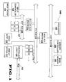
- the computer system 100 is an IBM-compatible, personal computer (PC) system or the like typically used for workstations or server systems.
- the computer system 100 includes a host bus 108 coupled to at least one central processing unit (CPU) identified as main processor 102.
- processor 102 preferably includes any one of several microprocessors and supporting external circuitry typically used in PCs, such as the 80386, 80486, PentiumTM, Pentium IITM, etc. microprocessors from Intel Corp., where the external circuitry preferably includes an external or level two (L2) cache or the like (not shown).
- L2 level two
- a memory controller 104 is coupled to the host bus 108 and to the main memory 106 to receive and control main memory operations.
- the main memory 106 is coupled to the host bus 108 via buffers (not shown) for data transfer.
- the main memory 106 is preferably implemented with one or more memory boards plugged into compatible memory slots on the motherboard, although any main memory configuration is contemplated.
- the computer system 100 includes a PCI bus 112 coupled to the host bus 108 via a Host-PCI bridge 110, which handles translation of signals between the host bus 108 and the PCI bus 112.
- the PCI bus 112 is typically implemented with one or more PCI slots 116, individually labeled S1, S2, S3 and so on, where each of the PCI slots 116 are configured to receive compatible PCI adapter cards incorporating one or more PCI devices as known to those skilled in the art.
- Typical PCI devices include network interface cards (NICs) disk controllers such as a SCSI (Small Computer System Interface) disk controller, video or graphics controllers, etc.
- NICs network interface cards
- SCSI Small Computer System Interface
- the isolation system according to the present invention is used within an array controller, such as each array controller 132 of Fig. 2. It should be understood that the present isolation system could otherwise be carried out in any system which includes a low voltage device and other devices that operate at a voltage that is higher than the maximum operating voltage of the low voltage device, so that it is desired to isolate the low voltage device.
- a controller card 120 is used to interface between the system PCI bus 112 and an array controller 132.
- the controller card 120 is fashioned as a PCI card that is plugged into one of the PCI slots 116.
- the controller card 120 interfaces between the PCI bus 112 and a communication bus 122, which in one embodiment is a fiber optic cable or link.
- Bus 122 in turn communicates with the disk drive storage units 130 (Fig. 2). It should be understood that bus 122 need not be a fiber optic link, but instead may be any commonly used electrical conductor such as a coaxial cable, a ribbon wire cable assembly, or other similar device used to bus electrical signals between one or more points in a computer system. Bus 122 is implemented as a fiber optic link to allow for greater bandwidth between the computer system 100 and a plurality of peripheral devices, typically disk drives.
- the embodiment depicted utilizes an input device 126, such as a mouse, keyboard, light pen, pointing device or any other similar type user input device known to those skilled in the art.
- the input device 126 is coupled to a corresponding input controller 124 which can be coupled to PCI bus 112 or is otherwise coupled to an expansion bus 128, depending on the particular system implementation.
- the computer system 100 also includes a display device 117, such as a monitor or the like, which is coupled to a video controller 118 which is coupled to the PCI bus 112.
- a configuration utility is loaded into the main memory 106 and is executed by the processor 102, which facilitates configuration of a drive array using the disk drives shown in Fig. 2.
- the computer system 100 may be implemented in any one of many alternative manners.
- an industry standard architecture (ISA) bus or an extended ISA (EISA) bus could be substituted for the PCI bus 112.
- EISA EISA bus
- the Host-PCI bridge 110 would be replaced by an EISA bus controller (EBC) for handling transitions of signals between the host bus 108 and an EISA bus.
- EBC EISA bus controller
- the PCI slots 116 are instead EISA slots for receiving EISA compatible cards, and the controller card 120 is replaced by a corresponding array controller card implemented for interfacing an EISA bus.
- the computer system 100 includes the expansion bus 128 coupled to the primary PCI bus 112 through a PCI-expansion bus bridge 114.
- the expansion bus 114 is any one of many different types, including another PCI bus, an ISA bus, an EISA bus or the microchannel architecture (MCA) bus, among others.
- the PC-expansion bus bridge 114 is a PC-EISA bridge.
- the expansion bus 128 preferably includes one or more expansion or input/output (I/O) slots 127, individually labeled I1, I2, I3, etc.
- An array controller configured for plugging into one of the slots 127 and for interfacing the expansion bus 128 could be used instead of the controller card 120, where such controller card would interface with bus 122.
- the computer system 100 may include an integrated system peripheral (ISP), an interrupt controller such as an advanced programmable interrupt controller (APIC) or the like, arbiter(s), a system ROM (read only memory) comprising one or more ROM modules, a keyboard controller, a real time clock (RTC) and timers, communication ports, non-volatile static random access memory (NVSRAM), a direct memory access (DMA) system, diagnostics ports, command/status registers, battery-backed CMOS memory, etc.
- ISP integrated system peripheral
- APIC advanced programmable interrupt controller
- arbiter(s) a system ROM (read only memory) comprising one or more ROM modules
- a keyboard controller a real time clock (RTC) and timers
- RTC real time clock
- NVSRAM non-volatile static random access memory
- DMA direct memory access
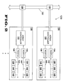
- the bus 122 couples the controller card 120 with a plurality of disk drive storage units 130 of a disk drive subsystem 129.
- Each disk drive storage unit 130 connects to bus 122 with a connector 135, which is a fiber optic connector if bus 122 is a fiber optic bus and is an electrical connector if bus 122 includes electrical signal conductors.
- Each disk drive storage unit 130 is physically a self-contained storage box that includes a backplane bus, which further includes SCSI buses 142, 143, although a single backplane SCSI bus is contemplated as well.
- Disk drive storage unit 130 also includes an array controller 132 which interfaces between bus 122 and SCSI ports A and B, 134 and 136, respectively.
- Each SCSI port 134, 136 is coupled to a unique SCSI bus 142, 143, respectively.
- a single SCSI port and a single SCSI bus may be utilized by the disk drive storage unit 130.
- Coupled to each SCSI bus 142, 143 is a plurality of physical drives 140.
- any disk controller may be used to control the plurality of disk drives in a disk drive storage unit 130, without the disk controller limited to being an array controller.
- the bus 122 may be a SCSI bus connected to a plurality of drives.
- the SCSI buses 142, 143 can be internal to the computer system 100 as desired rather than being provided in a separate drive subsystem 129.
- the array controller 132 and the disk drives 140 may be implemented according to SCSI-1 (ANSI X3,131-1986), SCSI-2 (ANSI X3.131-1994) including Fast SCSI, Wide SCSI-2 and Fast Wide SCSI or SCSI-3, which includes a plurality or family of standards including Fast-20 SCSI, Ultra SCSI, DoubleSpeed SCSI, etc.
- the array controller 132 and the drives 140 may alternatively be implemented according to any one of several disk drive implementations, such as the Integrated Drive Electronics (IDE), the AT Attachment (ATA) or ATA-2 or ATA-3, the enhanced-IDE (EIDE), the ATA Packet Interface (ATAPI), etc.
- the SCSI array controller 132 for each disk drive storage unit 130 operates the various attached SCSI drives 140 as an array of drives, preferably implementing striping and fault tolerant techniques such as RAID levels 1-5.
- a separate indicator light controller 138 is coupled to each of the SCSI buses 142, 143 for controlling indicator lights (not shown) representing status of each of the disk drives 140.
- a bridge 200 is provided for interfacing the bus 122 to a local bus 202, which is preferably a PCI local bus.
- the specific configuration of the bridge 200 depends upon the types of buses 122 and 202. Assuming that the bus 202 is a local PCI bus, then the bridge 200 is either an EISA to PCI bridge, a PCI to PCI bridge, a fiber optic to PCI bridge, etc.
- a PCI memory controller and XOR engine (WCXC) 210 is coupled between the PCI local bus 202 and a memory 211.
- the memory 211 preferably comprises dynamic RAM (DRAM) and includes a transfer buffer for temporary storage of disk data and/or command packets.
- DRAM dynamic RAM
- data read from any of the disk drives 140 may be temporarily stored within the memory 211 before being transferred to the main memory 106 via the bridge 200, and data to be written to the disk drives 140 from the main memory 106 may be temporarily stored in the memory 211.
- the memory 211 may further include cache memory and functions, battery backed, parity checked and mirrored memory for posted writes to the disk drives 140.
- the PCI local bus 202 is further coupled to two PCI SCSI controllers 212 and 214.
- the SCSI controller 212 is coupled to the disk drives 140 via the port 134 and the SCSI bus 142
- the SCSI controller 214 is coupled to the disk drives 140 via the port 136 and the SCSI bus 143. Any number Of PCI SCSI controllers may be included for coupling to corresponding SCSI ports and buses as desired.
- the array controller 132 preferably includes a local processor 205 coupled to a local processor bus 203, where the processor 205 is any type of suitable processor, such as the 29040 32-bit RISC processor by Advanced Micro Devices, Inc. (AMD).
- the processor 205 preferably operates at a low logic voltage level, such as 3.3 volts in the embodiment shown, but is tolerant to higher logic voltage levels, such as five (5) volt devices.
- a local processor interface (PDPI) 204 is coupled between the PCI local bus 202 and the bus 203 for interfacing the processor 205 to the PCI local bus 202.
- the processor 205 provides the main control for the array controller 132 for controlling configuration, data transfer, data organization, etc.
- the processor 205 is coupled to a local memory 206 and processor support circuitry 208 via the bus 203.
- the support circuitry 208 includes logic for providing support functionality for the processor 205, such as timers and interrupt controllers or the like.
- the support circuitry 208 includes at least one 5 volt device and the PDPI device 204 operates at 5 volts.
- the processor 205 is able to execute cycles on the bus 203 to access the support circuitry 208 and the PDPI device 204, since the processor 205 is 5 volt tolerant.
- the local memory 206 stores operating instructions for the local processor 205 and program memory for controlling operations of the processor 205. Instructions stored in the local memory 206 control the configuration and operation of the array controller 132 for storing data in and retrieving data from the disk drives 140.
- the memory 206 includes one or more 3.3 volt memory devices that are not tolerant to 5 volts. 5 volt signals applied to the memory 206 would otherwise damage or destroy the memory devices, so that the memory 206 should be isolated from the 5 volt devices accessing the bus 203. It is noted that although the present invention is illustrated using the 3.3 and 5 volt logic standards, that any two logic voltage standards are contemplated. Generally, the processor 205 operates according to the same logic voltage standard as the memory 206, but is tolerant to higher voltage devices. The higher voltage devices, however, operate at or above the maximum operating voltage of the memory 206.
- a switching device 224 is provided to electrically isolate the memory 206 from the processor bus 203 and thus any higher voltage devices.
- the processor 205 executes memory cycles on the bus 203 and asserts an address to access one or more memory locations within the memory 206 when the processor 205 needs to read data from or write data to the memory 206.
- Enable logic 222 coupled to the bus 203 detects the memory cycle and provides an ENABLE signal to a device enable (DE) input of the switching device 224 if the memory cycle is intended for the memory 206.
- the enable logic 222 typically decodes an address asserted on the bus 203 during the memory cycle.
- the switching device 224 electrically couples the memory 206 to the bus 203 so that the address is provided to the memory 206.
- the memory cycle includes a data portion so that data is written to or read from the memory 206.
- the bus 203 preferably includes address and data signals or combined address/data signals, which are coupled to corresponding address/data signals ofthe memory 206 when the switching device 224 is enabled.
- the switching device 224 preferably includes a plurality of first contacts coupled to signal contacts of the memory 206, and a plurality of corresponding second contacts coupled to corresponding bus signal lines of the bus 203.
- the switching device 224 further includes a plurality of switches, each coupled between corresponding ones of the first and second contacts of the switching device 224.
- the switches have at least two states based on the ENABLE signal received at the enable input (DE) of the switching device 224. A first "open” state disconnects the corresponding contacts of the switch and a second, “closed” state couples or electrically connects the corresponding contacts together.
- the switches of the switching device 224 are implemented in any suitable manner, such as relay type devices, bipolar transistors, field-effect transistors (FETs), metal oxide semiconductor FETs (MOSFETs), etc.
- the switching device 224 is preferably a high speed CMOS bus switch, such as the QS32X384 bus switch manufactured by Quality Semiconductor, Inc.
- the switching device 224 is an SN74CBTS3384 10-bit bus switch manufactured by Texas Instruments, Inc. (TI).
- the processor 205 may assert a cycle start signal along with control signals indicating the type of cycle on the bus 203.
- control signals indicating the type of cycle on the bus 203.
- an MIO signal may be provided that indicates whether the cycle is memory or input/output (I/O), and a read/write (R/W) signal may indicate whether the cycle is a read or write cycle, respectively.
- the processor 205 generally asserts control signals identifying the duration of each memory cycle, such as a cycle signal that is asserted during the duration of each cycle. Any one of several methods are contemplated and depends upon the particular processor, memory and implementation.
- the processor 205 asserts an address on the processor bus 203 that corresponds to the local memory 206.
- the memory 206 is mapped into a predetermined memory range of memory space of the processor 205.
- the enable logic 222 detects the memory cycle executed by the processor 205 and then decodes the address asserted on the bus 203. In particular, the enable logic 222 reads or otherwise latches the address and compares the address with the predetermined memory range. If the address indicates the memory 206, then the enable logic 222 generates or otherwise asserts the ENABLE signal.
- the ENABLE signal When the ENABLE signal is provided to the switching device 224, it transitions from an open or high impedance state to a closed or low impedance state, which electrically couples the signals of the memory 206 to the bus 203 to respond to the cycle executed by the processor 205.
- the other, higher voltage devices do not assert 5 volt signals on the bus 203.
- the 5 volt devices are placed in a high impedance or open circuited state or are otherwise temporarily disabled to prevent 5 volt signals on the bus 203. This prevents damage to the memory 206.
- Figure 4 depicts an embodiment of a memory isolation system according to the present invention used for a processor and main memory of a computer system.
- This embodiment which includes a 3.3 volt main processor 302, could be used for smaller computer systems requiring energy conservation, such as laptops or portable computer systems.
- a main processor 302 and a 5 volt device 311 are shown coupled to a host bus 308.
- the main processor 302 may be any one of several microprocessors and supporting external circuitry discussed above with regard to Fig. 3.
- the 5 volt device 311 may be a video controller for a video display device or any other type of 5 volt device coupled to the host bus of a computer system.
- a host-PCI bridge 310 functions as an interface between the host bus 308 and a PCI bus 312.
- Decode logic 309 is coupled to host bus 3 08 and to a switching device 3 05 via a device enable (DE) input of switching device 305.
- DE device enable
- the bridge 310 and the 5 volt device 311 each operate at logic voltage levels of 5 volts.
- Main processor 302 operates at 3.3 volts, but is 5 volt tolerant.
- the main memory 306, however, operates at 3.3 volts but is not 5 volt tolerant.
- the switching device 305 is utilized to electrically isolate main memory 306 from host bus 308 in a similar manner as the isolation system embodiment discussed above with reference to Fig. 3.
- the switching device 305 is preferably a high speed CMOS bus switch, such as the QS32X384 bus switch manufactured by Quality Semiconductor, Inc.
- the switching device 305 comprises relay(s), bipolar transistors, FET transistors, etc., or any other similar type electronic switches.
- the main processor 302 communicates over host bus 308 with other 5 volt devices coupled to host bus 308 other than main memory 306 while the main memory 306 remains isolated via the switching device 305. Since no device ENABLE signal is present, the switching device 305 is in an open position, essentially creating an open circuit or high impedance between each signal of the main memory 306 and corresponding signals of the bus 308. This electrically isolates main memory 306 from host bus 308 and the 5 volt communication present on host bus 308, which prevents main memory 306 from being damaged by any 5 volt signals present on bus 308.
- the main processor 302 executes a read or write memory cycle on bus 308 in a similar manner as described previously, and asserts an address corresponding to the memory 306.
- the memory 306 preferably corresponds to a range of addresses.
- the bridge 310 and the 5 volt device 311 do not assert 5 volt signals on the host bus 308.
- the decode logic 309 detects the memory cycle, decodes the memory address, and if the address is within the address range for the memory 306, the decode logic 309 asserts a device ENABLE signal to a DE input of the switching device 305.
- the switching device 305 transitions from an open, high impedance state, to a closed, low impedance state to electrically couple the signals of the memory 306 to corresponding signals of the host bus 308.
- the present invention is applicable for isolating any type of low voltage device that is coupled to a common interface with higher voltage devices, where it is desired to isolate the low voltage device from the higher voltage levels.
- the enable logic 222 or the decode logic 309 monitors any control, data or address signals or any combination thereof on a common interface, such as a bus or the like, to determine whether the low voltage device is being accessed.
- FIG. 5 is a schematic diagram of an exemplary embodiment of a switching device 500 that could be used with an isolation system according to the present invention.
- a plurality of individual field-effect transistor (FET) switches 230 are shown, each including drain and source terminals 234 and 235 and a gate terminal coupled to the output of a buffer inverter 232.
- a signal ENABLE* is provided to the input of the buffer inverter 232, where an asterisk at the end of a signal name denotes negative logic.
- a plurality of signals A0-A15 are provided to respective ones of the terminals 234, and a plurality of signals B0-B 15 are provided to respective ones of the terminals 235 of the FET switches 230.
- the buffer inverter 232 When the ENABLE* signal is negated high, the buffer inverter 232 assert its output low turning off the FET switches 230 causing a high impedance between the terminals 234, 235.
- the signals A0-A15 are electrically isolated from the B0-B15 signals.
- the buffer inverter 232 When the ENABLE* signal is asserted low, the buffer inverter 232 asserts its output high turning on all of the FET switches 230. When on, a very low impedance appears across the terminals 234, 235 of each the FET switches 232, thereby electrically coupling the A0-A15 signals to the B0-B15 signals, respectively.
- the buffer inverter 232 provides sufficient drive current to drive the gates of all of the FET switches 230. Alternatively, a plurality of buffers may be provided for driving selected ones of the FET switches 230.
- the A0-A15 signals could be corresponding address/data signals of the processor bus 203 shown in Figure 3, where the B0-B15 signals are the corresponding address/data signals of the memory 206.
- the A0-A15 signals could be corresponding address/data signals of the host bus 308 shown in Fig. 4, where the B0-B15 signals are the corresponding address/data signals ofthe main memory 306.
- the terminals 234, 235 are coupled to the corresponding signals of a bus and memory device, respectively, to achieve electrical isolation and protection of the memory device from harmful signals of the bus.
- the enable or decode logic enables electrical connection when a device addresses the memory, such as a processor or the like.
- a system and method according to the present invention solves the problem of having to electrically isolate a low voltage device from higher voltage devices coupled to a common interface.
- the present invention was illustrated in an embodiment for a main processor and main memory having a common bus, and in another embodiment for a drive array controller. However, it is understood that the present invention may be used in any electrical device where a low voltage device shares a common interface with other devices that operate at higher voltage levels that would otherwise damage the low voltage device.
Landscapes
- Engineering & Computer Science (AREA)
- General Engineering & Computer Science (AREA)
- Theoretical Computer Science (AREA)
- Computer Hardware Design (AREA)
- Physics & Mathematics (AREA)
- General Physics & Mathematics (AREA)
- Bus Control (AREA)
- Power Sources (AREA)
Applications Claiming Priority (2)
| Application Number | Priority Date | Filing Date | Title |
|---|---|---|---|
| US936208 | 1997-09-24 | ||
| US08/936,208 US6205500B1 (en) | 1997-09-24 | 1997-09-24 | System and method for electrically isolating a device from higher voltage devices |
Publications (1)
| Publication Number | Publication Date |
|---|---|
| EP0907129A1 true EP0907129A1 (fr) | 1999-04-07 |
Family
ID=25468328
Family Applications (1)
| Application Number | Title | Priority Date | Filing Date |
|---|---|---|---|
| EP19980307413 Withdrawn EP0907129A1 (fr) | 1997-09-24 | 1998-09-14 | Système et procédé d'isolation électrique entre un dispositif de bus et des dispositifs à tensions plus hautes |
Country Status (3)
| Country | Link |
|---|---|
| US (1) | US6205500B1 (fr) |
| EP (1) | EP0907129A1 (fr) |
| JP (1) | JPH11175208A (fr) |
Families Citing this family (9)
| Publication number | Priority date | Publication date | Assignee | Title |
|---|---|---|---|---|
| US6622250B1 (en) * | 1999-12-21 | 2003-09-16 | Intel Corporation | SMBUS over the PCI bus isolation scheme and circuit design |
| TW484723U (en) * | 2000-12-20 | 2002-04-21 | Areca Technology Corp | Disk array controller |
| US7162654B1 (en) * | 2001-01-04 | 2007-01-09 | 3Pardata, Inc. | Isolation of I2C buses in a multiple power domain environment using switches |
| US7028132B2 (en) * | 2001-09-29 | 2006-04-11 | Hewlett-Packard Development Company, L.P. | Distributed peer-to-peer communication for interconnect busses of a computer system |
| US6871248B2 (en) * | 2001-09-29 | 2005-03-22 | Hewlett-Packard Development Company, L.P. | Isochronous transactions for interconnect busses of a computer system |
| US6928509B2 (en) * | 2002-08-01 | 2005-08-09 | International Business Machines Corporation | Method and apparatus for enhancing reliability and scalability of serial storage devices |
| WO2005008409A2 (fr) * | 2003-07-11 | 2005-01-27 | Digitalnet Government Solutions, Llc | Commutateur clavier-ecran-souris a haut degre d'isolation |
| US9201790B2 (en) * | 2007-10-09 | 2015-12-01 | Seagate Technology Llc | System and method of matching data rates |
| US8430576B2 (en) * | 2011-03-15 | 2013-04-30 | Intel Corporation | Fiber termination in light peak lenses |
Citations (3)
| Publication number | Priority date | Publication date | Assignee | Title |
|---|---|---|---|---|
| US5229652A (en) * | 1992-04-20 | 1993-07-20 | Hough Wayne E | Non-contact data and power connector for computer based modules |
| EP0674274A1 (fr) * | 1994-03-24 | 1995-09-27 | International Computers Limited | Système pour isoler des unités de fond de panier |
| EP0788058A1 (fr) * | 1996-02-05 | 1997-08-06 | Motorola, Inc. | Système de traitement de données à faible consommation pour faire l'interfaçage à un dispositif externe et procédé associé |
Family Cites Families (28)
| Publication number | Priority date | Publication date | Assignee | Title |
|---|---|---|---|---|
| GB674274A (en) | 1950-01-21 | 1952-06-18 | Arthur James Simpson | Improvements in or relating to liquid proportioning valves |
| GB788058A (en) | 1953-08-17 | 1957-12-23 | Air Preheater | Electrostatic precipitator supply control circuits |
| US4481430A (en) * | 1982-08-02 | 1984-11-06 | Fairchild Camera & Instrument Corp. | Power supply threshold activation circuit |
| US4964011A (en) * | 1989-05-22 | 1990-10-16 | Databook, Inc. | Voltage transient protection circuit |
| US5317721A (en) * | 1989-11-06 | 1994-05-31 | Zenith Data Systems Corporation | Method and apparatus to disable ISA devices for EISA addresses outside the ISA range |
| EP0447145B1 (fr) * | 1990-03-12 | 2000-07-12 | Hewlett-Packard Company | Accès direct mémoire planifié par l'usager utilisant des adresses virtuelles |
| US5625593A (en) * | 1990-03-28 | 1997-04-29 | Mitsubishi Denki Kabushiki Kaisha | Memory card circuit with separate buffer chips |
| JP3063334B2 (ja) * | 1991-12-19 | 2000-07-12 | 日本電気株式会社 | 高信頼度化情報処理装置 |
| US5265211A (en) * | 1992-01-02 | 1993-11-23 | International Business Machines Corporation | Arbitration control logic for computer system having dual bus architecture |
| US5592415A (en) * | 1992-07-06 | 1997-01-07 | Hitachi, Ltd. | Non-volatile semiconductor memory |
| US5559966A (en) * | 1992-11-06 | 1996-09-24 | Intel Corporation | Method and apparatus for interfacing a bus that operates at a plurality of operating potentials |
| US5365181A (en) * | 1993-03-15 | 1994-11-15 | Texas Instruments Incorporated | Frequency doubler having adaptive biasing |
| US5467453A (en) * | 1993-07-20 | 1995-11-14 | Dell Usa, L.P. | Circuit for providing automatic SCSI bus termination |
| DE69433320T2 (de) * | 1993-07-29 | 2004-09-16 | Atmel Corp., San Jose | Ferngesteuerter rreprogrammierbarer programmspeicher fuer einen mikrokontroller |
| US5563838A (en) * | 1994-02-01 | 1996-10-08 | Micron Electronics, Inc. | Module having voltage control circuit to reduce surges in potential |
| US5596708A (en) * | 1994-04-04 | 1997-01-21 | At&T Global Information Solutions Company | Method and apparatus for the protection of write data in a disk array |
| US5497119A (en) * | 1994-06-01 | 1996-03-05 | Intel Corporation | High precision voltage regulation circuit for programming multilevel flash memory |
| TW289153B (fr) * | 1994-09-26 | 1996-10-21 | Ibm | |
| US5671179A (en) * | 1994-10-19 | 1997-09-23 | Intel Corporation | Low power pulse generator for smart voltage flash eeprom |
| US5557758A (en) * | 1994-11-30 | 1996-09-17 | International Business Machines Corporation | Bridge between two buses of a computer system that determines the location of memory or accesses from bus masters on one of the buses |
| CA2142644C (fr) * | 1995-02-16 | 1996-11-26 | Marc Etienne Bonneville | Circuit d'alimentation de secours |
| US5822512A (en) * | 1995-05-19 | 1998-10-13 | Compaq Computer Corporartion | Switching control in a fault tolerant system |
| US5561384A (en) * | 1995-11-08 | 1996-10-01 | Advanced Micro Devices, Inc. | Input/output driver circuit for isolating with minimal power consumption a peripheral component from a core section |
| US5796992A (en) * | 1995-12-20 | 1998-08-18 | Compaq Computer Corporation | Circuit for switching between synchronous and asynchronous memory refresh cycles in low power mode |
| US5680063A (en) * | 1996-04-23 | 1997-10-21 | Motorola, Inc. | Bi-directional voltage translator |
| US5822547A (en) * | 1996-05-31 | 1998-10-13 | Texas Instruments Incorporated | Method and apparatus for providing a portable computer with hot pluggable modular bays |
| US5943482A (en) * | 1996-06-05 | 1999-08-24 | Compaq Computer Corporation | Expansion card insertion and removal |
| US5938751A (en) * | 1997-08-15 | 1999-08-17 | Compaq Computer Corporation | Bus ring-back and voltage over-shoot reduction techniques coupled with hot-pluggability |
-
1997
- 1997-09-24 US US08/936,208 patent/US6205500B1/en not_active Expired - Lifetime
-
1998
- 1998-09-14 EP EP19980307413 patent/EP0907129A1/fr not_active Withdrawn
- 1998-09-18 JP JP26482598A patent/JPH11175208A/ja active Pending
Patent Citations (3)
| Publication number | Priority date | Publication date | Assignee | Title |
|---|---|---|---|---|
| US5229652A (en) * | 1992-04-20 | 1993-07-20 | Hough Wayne E | Non-contact data and power connector for computer based modules |
| EP0674274A1 (fr) * | 1994-03-24 | 1995-09-27 | International Computers Limited | Système pour isoler des unités de fond de panier |
| EP0788058A1 (fr) * | 1996-02-05 | 1997-08-06 | Motorola, Inc. | Système de traitement de données à faible consommation pour faire l'interfaçage à un dispositif externe et procédé associé |
Also Published As
| Publication number | Publication date |
|---|---|
| JPH11175208A (ja) | 1999-07-02 |
| US6205500B1 (en) | 2001-03-20 |
Similar Documents
| Publication | Publication Date | Title |
|---|---|---|
| US6845420B2 (en) | System for supporting both serial and parallel storage devices on a connector | |
| US5664124A (en) | Bridge between two buses of a computer system that latches signals from the bus for use on the bridge and responds according to the bus protocols | |
| US5875308A (en) | Peripheral component interconnect (PCI) architecture having hot-plugging capability for a data-processing system | |
| US6567876B1 (en) | Docking PCI to PCI bridge using IEEE 1394 link | |
| EP1038231B1 (fr) | Mecanisme d'execution du reacheminement de destination d'interruption | |
| US5938751A (en) | Bus ring-back and voltage over-shoot reduction techniques coupled with hot-pluggability | |
| US6163824A (en) | Hot plug port adapter with separate PCI local bus and auxiliary bus | |
| US5748912A (en) | User-removable central processing unit card for an electrical device | |
| US6064626A (en) | Peripheral buses for integrated circuit | |
| US5109517A (en) | System for selectively controlling slots in an IBM-AT/NEC 9801 dual-compatible computer | |
| CA2143492A1 (fr) | Interface pcmcia portative pour ordinateur hote | |
| US6532500B1 (en) | System and method to support out-band storage subsystem management via SCSI bus when operating power to a computer system is off | |
| US20040078716A1 (en) | Extended host controller test mode support | |
| US6205500B1 (en) | System and method for electrically isolating a device from higher voltage devices | |
| US6079024A (en) | Bus interface unit having selectively enabled buffers | |
| EP0493888B1 (fr) | Ordinateur personnel avec possibilité d'extension de la mémoire locale | |
| US5187781A (en) | Shared hardware interrupt circuit for personal computers | |
| EP0797148A1 (fr) | Structure d'antémémoire multi-mode | |
| US5485585A (en) | Personal computer with alternate system controller and register for identifying active system controller | |
| US5734844A (en) | Bidirectional single-line handshake with both devices driving the line in the same state for hand-off | |
| JP3782226B2 (ja) | コンピュータシステムおよびusbコントローラ | |
| KR101118558B1 (ko) | Usb otg 제어기 | |
| EP0487910A1 (fr) | Ordinateur portable avec un cycle de lecture/d'écriture variable selon le type de carte mémoire | |
| US20060095626A1 (en) | Multifunction adapter | |
| CN1237458C (zh) | 接口设备及包含该设备的信息处理系统 |
Legal Events
| Date | Code | Title | Description |
|---|---|---|---|
| PUAI | Public reference made under article 153(3) epc to a published international application that has entered the european phase |
Free format text: ORIGINAL CODE: 0009012 |
|
| AK | Designated contracting states |
Kind code of ref document: A1 Designated state(s): AT BE CH CY DE DK ES FI FR GB GR IE IT LI LU MC NL PT SE |
|
| AX | Request for extension of the european patent |
Free format text: AL;LT;LV;MK;RO;SI |
|
| AKX | Designation fees paid | ||
| STAA | Information on the status of an ep patent application or granted ep patent |
Free format text: STATUS: THE APPLICATION IS DEEMED TO BE WITHDRAWN |
|
| 18D | Application deemed to be withdrawn |
Effective date: 19991008 |
|
| REG | Reference to a national code |
Ref country code: DE Ref legal event code: 8566 |