EP0907124A1 - Microcomputer and electronic equipment - Google Patents
Microcomputer and electronic equipment Download PDFInfo
- Publication number
- EP0907124A1 EP0907124A1 EP98911056A EP98911056A EP0907124A1 EP 0907124 A1 EP0907124 A1 EP 0907124A1 EP 98911056 A EP98911056 A EP 98911056A EP 98911056 A EP98911056 A EP 98911056A EP 0907124 A1 EP0907124 A1 EP 0907124A1
- Authority
- EP
- European Patent Office
- Prior art keywords
- microcomputer
- address
- instruction
- resetting
- program
- Prior art date
- Legal status (The legal status is an assumption and is not a legal conclusion. Google has not performed a legal analysis and makes no representation as to the accuracy of the status listed.)
- Withdrawn
Links
Images


Classifications
-
- G—PHYSICS
- G06—COMPUTING OR CALCULATING; COUNTING
- G06F—ELECTRIC DIGITAL DATA PROCESSING
- G06F9/00—Arrangements for program control, e.g. control units
- G06F9/06—Arrangements for program control, e.g. control units using stored programs, i.e. using an internal store of processing equipment to receive or retain programs
- G06F9/44—Arrangements for executing specific programs
- G06F9/4401—Bootstrapping
- G06F9/4403—Processor initialisation
-
- G—PHYSICS
- G06—COMPUTING OR CALCULATING; COUNTING
- G06F—ELECTRIC DIGITAL DATA PROCESSING
- G06F9/00—Arrangements for program control, e.g. control units
- G06F9/06—Arrangements for program control, e.g. control units using stored programs, i.e. using an internal store of processing equipment to receive or retain programs
- G06F9/44—Arrangements for executing specific programs
- G06F9/4401—Bootstrapping
- G06F9/4406—Loading of operating system
Definitions
- the present invention relates to a microcomputer and electronic equipment.
- such a microcomputer is provided with a ROM inside, i.e., an internal ROM.
- the internal ROM stores a user-generated program, and after the microcomputer is reset, a reset processing program (a program to be executed first after resetting) contained in the internal ROM is usually called into execution first.
- the internal ROM is a mask ROM and therefore a certain period of time (turnaround time) is required after completion of a mask pattern design until delivery of IC to engineers.
- a certain period of time is required after completion of a mask pattern design until delivery of IC to engineers.
- an external ROM such as EPROM or EEPROM allowing the rewriting of data in a relatively brief period of time instead of the internal ROM.
- Some users employ only the external ROM for giving priority to prompt countermeasures against a possible defect in a product, i.e., it is not desirable to use the internal ROM in some cases.
- a microcomputer of the present invention comprises: a control circuit for reading an instruction, analyzing the instruction and controlling execution thereof; a given changeover terminal; and a changeover circuit for switching a boot address to be read first by the control circuit after resetting according to the state of the changeover terminal.
- the control circuit if the changeover terminal is in the first state for example, the control circuit reads an instruction and its address from a first boot address after resetting. The control circuit therefore starts instruction execution according to the program stored at the first boot address. In contrast, if the changeover terminal is in the second state, the control circuit reads out an instruction and its address from a second boot address. In this case, the control circuit therefore starts instruction execution according to the program stored at the second boot address. More specifically, in the present invention, it is possible to select the location in which a program to be carried out first after resetting is stored. This means that the users can select an arbitrary startup location for the program to be executed first after resetting, thus enhancing user convenience substantially.
- a top instruction of the program to be executed first after resetting may be stored at the boot address, or a jump instruction to an address of a top instruction of the program to be executed first after resetting may be stored at the boot address. Further, an address of a top instruction of the program to be executed first after resetting may be stored at the boot address.
- the boot address may be an address of the internal ROM incorporated in the microcomputer when the changeover terminal is in the first state; and the boot address may be an address of the external ROM disposed outside the microcomputer when the changeover terminal is in the second state.
- the user can determine arbitrarily whether the program is to be started from the internal ROM or the external ROM, thus improving user convenience significantly.
- Electronic equipment of the present invention comprises: the aforementioned microcomputer; an input data source for supplying data to be processed by the microcomputer; and an output apparatus for outputting data processed by the microcomputer.
- a system can be configured without using an external or internal memory as desired thus reducing cost, physical size, consumption of power, and development time of the electronic equipment.
- Figure 1 shows a block diagram of the microcomputer 101 in the present embodiment.
- the microcomputer 101 shown in Figure 1 comprises a CPU 102 (control circuit) for processing 32-bit data for example, a bus control unit (BCU) 108 for controlling a bus, and an internal memory 110 including an internal ROM 112.
- a CPU 102 control circuit
- BCU bus control unit
- internal memory 110 including an internal ROM 112.
- an external memory 114 Disposed outside the microcomputer 101 is an external memory 114 including an external ROM 116.
- the CPU 102 receives instructions from the internal memory 110 or the external memory 114, analyzes them, and controls processing for executing the analyzed instructions.
- an instruction having a length of 16 bits is used.
- the CPU 102 comprises an instruction decoder 118 for analyzing an instruction from the instruction data bus, a program counter (PC) 120, a general-purpose register block 103 having sixteen 32-bit registers R0 to R15, a sum-of-products operation circuit 104 for performing sum-of-products calculations, and an arithmetic and logic unit (ALU) 106 for performing arithmetic calculations such as addition, subtraction, multiplication and division on data and logical operations such as logical ORing, logical ANDing and logical shifting.
- the sum-of-products operation circuit 104 carries out sum-of-products calculations, and the ALU 106 carries out various calculations.
- the instruction decoder 118 includes a changeover circuit 150.
- the general-purpose register block 103, the sum-of-products operation circuit 104 and the ALU 106 send or receive data through a CPU internal bus.
- the BCU 108 performs bus control for reading various instructions and various data necessary for execution thereof from the internal memory 110 or the external memory 114 and for writing data to the internal memory 110 or the external memory 114.
- the microcomputer 101 is provided with a changeover terminal BTA3 and a changeover circuit 150 for switching a boot address to be read first by the CPU 102 after resetting, according to the state of the changeover terminal BTA3.
- the user can determine whether a program startup after resetting is to be made from the internal ROM 112 or the external ROM 116.
- a reset processing program to be executed first after resetting is stored in the internal ROM 112 and the changeover terminal BTA3 is set to state '1' (high level), for instance.
- a boot address generated by the changeover circuit 150 after resetting is an address of the internal ROM 112, and the CPU 102 reads this boot address after resetting. Therefore, if the boot address is set at the top address location of the reset processing program, for example, the program is started from the internal ROM 112.
- the reset processing program is stored in the external ROM 116 and BTA3 is set to state '0' (low level), for instance.
- a boot address generated by the changeover circuit 150 after resetting is an address of the external ROM 116, and the CPU 102 reads this boot address after resetting. Therefore, if the boot address is set at the top address location of the reset processing program, for example, the program is started from the external ROM 116.
- the top instruction of the reset processing program to be executed first after resetting is stored at a boot address.
- the boot address itself is the top address of the reset processing program.
- the top instruction is read according to the boot address to start execution of the reset processing program.
- a jump instruction instructing to jump to an address of the top instruction of the reset processing program (or top address of the reset processing program) is stored at a boot address.
- the jump instruction is read according to the boot address, the jump instruction is carried out to read the top instruction of the reset processing program, and then execution of the reset processing program is started.
- an address of the top instruction of the reset processing program is stored at a boot address. In this case, therefore, the address of the top instruction is read according to the boot address. Then, according to the read address, the top instruction is read out to start execution of the reset processing program.
- the technique shown in Figure 2B requires four to six bits for a jump instruction operation code, for example. Therefore, the number of bits available for specifying a jump address is limited to 26 to 28 bits.
- the technique shown in Figure 2C has the advantage that all 32 bits can be used for addressing.
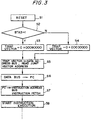
- the trap vector thus generated is output to a data address bus, and then a jump vector address is read (step S5). For instance, if BTA3 is set to state '1' and a trap vector of 0x00080000 is generated, a jump vector address of 0x00080100 is read from a trap vector table contained in the internal ROM 112. In contrast, if BTA3 is set to state '0' and a trap vector of 0x00C00000 is generated, a jump vector address of 0x00C00100 is read from a trap vector table contained in the external ROM 116.
- the jump vector address thus read is input to the PC 120 through a data bus (step S6).
- the jump vector address is set in the PC 120. For instance, if BTA3 is in state '1', a jump vector address of 0x00080100 (or a top address of the reset processing program stored in the internal ROM) is set in the PC 120. If BTA3 is in state '0', a jump vector address of 0x00C00100 (or a top address of the reset processing program stored in the external ROM) is set in the PC 120.
- the jump vector address When the jump vector address is set in the PC 120, it is output from the PC 120 to an instruction address bus. Then, the top instruction of the reset processing program is fetched (step S7). For instance, if BTA3 is in state '1', the top instruction of the reset processing program stored in the internal ROM 112 is fetched. If BTA3 is in state '0', the top instruction of the reset processing program stored in the external ROM 116 is fetched. Upon receiving the top instruction, the instruction decoder 118 analyzes this instruction to start instruction execution (step S8). At this step of the operation, the address of the top instruction of the reset processing program (or a jump vector address) is set in the PC 120. Therefore, when execution of the top instruction is completed and the program count is incremented, the PC 120 indicates the next instruction following the top instruction. Thus, execution of the next instruction is enabled.
- the user can select an arbitrary program startup location after resetting.
- BTA3 is set to state '1' and the reset processing program is stored in the internal ROM 112.
- a desired jump vector address is stored at the address 0x00080000 and the reset processing program is stored at a location corresponding to this jump vector address.
- the program can be started from the internal ROM 112, thereby eliminating the need for providing the external ROM 116 outside the microcomputer 101. This reduces cost, size, and power consumption of the electronic equipment containing the microcomputer 101.
- the external ROM 116 may be required only for the purpose of starting the reset processing program, resulting in a disadvantage such as an increase cost of the electronic equipment. According to the present embodiment, it becomes possible to overcome this disadvantage.
- BTA3 is set to state '0' and the reset processing program is stored in the external ROM 116.
- a desired jump vector address is stored at the address 0x00C00000 and the reset processing program is stored at a location corresponding to this jump vector address.
- the changeover terminal BTA3 is set to state '1' so that a program startup can be made from the internal ROM 112.
- BTA3 is always set to state '0'.
- the second embodiment presents a detailed example of a microcomputer in accordance with this invention.
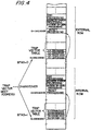
- a microcomputer 700 of the second embodiment is a 32-bit microcomputer, which comprises: a CPU 710; a ROM 720; a RAM 730; a high-frequency oscillator circuit 910; a low-frequency oscillator circuit 920; a reset circuit 930; a prescaler 940; a timer circuit including a 16-bit programmable timer 950, 8-bit programmable timer 960 and clock timer 970; a data transfer control circuit including an intelligent DMA 980 and high-speed DMA 990; an interrupt controller 800; a serial interface 810; a BCU 740; an analog interface circuit including an A/D converter 830 and D/A converter 840; an I/O circuit including an input port 850, output port 860 and I/O port 870; various buses 750 and 760 for connecting these circuits; and various terminals 890 including a BTA3 terminal.
- the microcomputer 700 formed on one chip of a semiconductor substrate is of an RISC type that is capable of processing 32-bit data. Using a pipelined architecture and load store architecture, the microcomputer 700 carries out virtually every instruction in a one clock cycle. All the instructions are described in a fixed length of 16 bits, thus substantially reducing the instruction code size.
- the third embodiment is concerned with electronic equipment containing the microcomputer mentioned in the first and second embodiments.
- the microcomputer in these embodiments allows the user to select an arbitrary program startup location after resetting through use of the changeover terminal BTA3.
- the embodiment of electronic equipment containing such a microcomputer it becomes possible to reduce the cost, physical size and power consumption and shorten the development period.
- Figure 6A shows an internal block diagram of a car navigation system, which is an example of the electronic equipment, and Figure 7A gives an external view.
- the car navigation system is operated using a remote controller 510, and a position detector section 520 determines the location of the car according to information received from the global positioning system (GPS) or gyrocompass system. Map information is stored on a CDROM 530 (information storage medium).
- An image memory 540 serves as a working area for image processing, and the image generated is displayed through an image output section 550 so that the driver can view it.
- a microcomputer 500 receives data from such input data sources as the remote controller 510, position detector section 520 and CDROM 530, carries out various types of processing, and outputs processed data through an output apparatus such as the image output section 550.
- Figure 6B shows an internal block diagram of a game machine, which is another example of the electronic equipment, and Figure 7B gives an external view.
- a game machine exemplified here, according to player control information from a game controller 560, a game program from a CDROM 570 and player information from an IC card 580, a game image and sound are generated using an image memory 590 as a working area. These are output through an image output section 610 and a sound output section 600.
- Figure 6C shows an internal block diagram of a printer, which is another example of electronic equipment, and Figure 7C gives the external view.
- a print image is generated using a bit-map memory 650 as a working area and this image is output through a print output section 660.
- a printer status and operation mode is indicated to the user on a display panel 670.
- the microcomputer of the present invention is applicable to a variety of electronic equipment including; a mobile telephone (cellular phone), PHS telephone, pager, audio equipment, electronic notebook, electronic calculator, POS terminal, touch-panel-equipped device, projector, word processor, personal computer, television set, video tape recorder with viewfinder/direct-view monitor, and the like.
- a mobile telephone cellular phone
- PHS telephone pager
- audio equipment electronic notebook
- electronic calculator electronic calculator
- POS terminal touch-panel-equipped device
- projector word processor
- personal computer television set, video tape recorder with viewfinder/direct-view monitor, and the like.
- the changeover terminal BTA3 is used for determining whether a program startup is to be made from the internal ROM or the external ROM.
- the present invention is particularly useful in the case where such a changeover is performed, the invention is not limited thereto but may be practiced or embodied in still other ways using any provision for switching a boot address to be read first by the CPU (control circuit) after resetting according to the state of the changeover terminal.
- An arrangement may also be provided so that two bits or more are assigned to the changeover terminal.
- the present invention is not limited in its application to the techniques shown in Figures 2A, 2B and 2C for starting execution of the reset processing program using a boot address.
Landscapes
- Engineering & Computer Science (AREA)
- Software Systems (AREA)
- Theoretical Computer Science (AREA)
- Physics & Mathematics (AREA)
- General Engineering & Computer Science (AREA)
- General Physics & Mathematics (AREA)
- Computer Security & Cryptography (AREA)
- Microcomputers (AREA)
- Complex Calculations (AREA)
Abstract
Description
Claims (6)
- A microcomputer comprising:a control circuit for reading an instruction, analyzing said instruction and controlling execution of said instruction;a given changeover terminal; anda changeover circuit for switching a boot address to be read first by said control circuit after resetting, according to the state of said changeover terminal.
- The microcomputer as defined in claim 1,
wherein a top instruction of a program to be executed first after resetting is stored at said boot address. - The microcomputer as defined in claim 1,
wherein a jump instruction to an address of a top instruction of a program to be executed first after resetting is stored at said boot address. - The microcomputer as defined in claim 1,
wherein an address of a top instruction of a program to be executed first after resetting is stored at said boot address. - The microcomputer as defined in claim 1,
wherein said boot address is an address of an internal ROM incorporated in said microcomputer when said changeover terminal is in a first state; and
wherein said boot address is an address of an external ROM disposed outside said microcomputer when said changeover terminal is in a second state. - Electronic equipment comprising:the microcomputer as defined in any one of claims 1 to 5;an input data source for supplying data to be processed by said microcomputer; andan output apparatus for outputting data processed by said microcomputer.
Applications Claiming Priority (3)
| Application Number | Priority Date | Filing Date | Title |
|---|---|---|---|
| JP9645397 | 1997-03-31 | ||
| JP96453/97 | 1997-03-31 | ||
| PCT/JP1998/001393 WO1998044408A1 (en) | 1997-03-31 | 1998-03-27 | Microcomputer and electronic equipment |
Publications (2)
| Publication Number | Publication Date |
|---|---|
| EP0907124A1 true EP0907124A1 (en) | 1999-04-07 |
| EP0907124A4 EP0907124A4 (en) | 2001-11-28 |
Family
ID=14165451
Family Applications (1)
| Application Number | Title | Priority Date | Filing Date |
|---|---|---|---|
| EP98911056A Withdrawn EP0907124A4 (en) | 1997-03-31 | 1998-03-27 | MICROCOMPUTER AND ELECTRONIC EQUIPMENT |
Country Status (4)
| Country | Link |
|---|---|
| EP (1) | EP0907124A4 (en) |
| KR (1) | KR20000016163A (en) |
| TW (1) | TW366471B (en) |
| WO (1) | WO1998044408A1 (en) |
Cited By (3)
| Publication number | Priority date | Publication date | Assignee | Title |
|---|---|---|---|---|
| WO2001057658A3 (en) * | 2000-02-04 | 2002-04-18 | Insyde Software Inc | A system and method for altering an operating system start-up sequence prior to operating system loading |
| WO2002048860A3 (en) * | 2000-12-14 | 2002-11-14 | Psion Digital Ltd | Synchronous memory controller |
| DE10255539A1 (en) * | 2002-11-28 | 2004-06-24 | Abb Patent Gmbh | Harvard-architecture microcomputer commissioning method in which an external program memory is connected to the microcomputer and used to reprogram the appropriate program data memory |
Family Cites Families (4)
| Publication number | Priority date | Publication date | Assignee | Title |
|---|---|---|---|---|
| JPH0212330A (en) * | 1988-06-29 | 1990-01-17 | Nec Corp | Microprocessor control system |
| JPH0581446A (en) * | 1991-09-20 | 1993-04-02 | Fujitsu Ltd | Internal/external rom switching system for microcontroller |
| TW241346B (en) * | 1991-10-15 | 1995-02-21 | Bull Hn Information Syst | |
| US5432927A (en) * | 1992-06-17 | 1995-07-11 | Eaton Corporation | Fail-safe EEPROM based rewritable boot system |
-
1998
- 1998-03-27 EP EP98911056A patent/EP0907124A4/en not_active Withdrawn
- 1998-03-27 KR KR1019980709731A patent/KR20000016163A/en not_active Withdrawn
- 1998-03-27 WO PCT/JP1998/001393 patent/WO1998044408A1/en not_active Ceased
- 1998-03-31 TW TW087104831A patent/TW366471B/en active
Cited By (4)
| Publication number | Priority date | Publication date | Assignee | Title |
|---|---|---|---|---|
| WO2001057658A3 (en) * | 2000-02-04 | 2002-04-18 | Insyde Software Inc | A system and method for altering an operating system start-up sequence prior to operating system loading |
| US6785808B2 (en) | 2000-02-04 | 2004-08-31 | Insyde Software, Inc. | System and method for altering an operating system start-up sequence prior to operating system loading |
| WO2002048860A3 (en) * | 2000-12-14 | 2002-11-14 | Psion Digital Ltd | Synchronous memory controller |
| DE10255539A1 (en) * | 2002-11-28 | 2004-06-24 | Abb Patent Gmbh | Harvard-architecture microcomputer commissioning method in which an external program memory is connected to the microcomputer and used to reprogram the appropriate program data memory |
Also Published As
| Publication number | Publication date |
|---|---|
| KR20000016163A (en) | 2000-03-25 |
| WO1998044408A1 (en) | 1998-10-08 |
| TW366471B (en) | 1999-08-11 |
| EP0907124A4 (en) | 2001-11-28 |
Similar Documents
| Publication | Publication Date | Title |
|---|---|---|
| US7340589B2 (en) | Shift prefix instruction decoder for modifying register information necessary for decoding the target instruction | |
| US20090235052A1 (en) | Data Processing Device and Electronic Equipment | |
| EP1012735B1 (en) | Eight-bit microcontroller having a risc architecture | |
| US6915413B2 (en) | Micro-controller for reading out compressed instruction code and program memory for compressing instruction code and storing therein | |
| TW201530320A (en) | Data processing apparatus and semiconductor integrated circuit device | |
| US5502827A (en) | Pipelined data processor for floating point and integer operation with exception handling | |
| US6233596B1 (en) | Multiple sum-of-products circuit and its use in electronic equipment and microcomputers | |
| JP2001504959A (en) | 8-bit microcontroller with RISC architecture | |
| US6986028B2 (en) | Repeat block with zero cycle overhead nesting | |
| US5410660A (en) | System and method for executing branch on bit set/clear instructions using microprogramming flow | |
| US7103759B1 (en) | Microcontroller architecture supporting microcode-implemented peripheral devices | |
| JPH081604B2 (en) | Microprocessor | |
| EP0907124A1 (en) | Microcomputer and electronic equipment | |
| JP3831396B2 (en) | Data processing apparatus and IC card | |
| JP4284559B2 (en) | Microprocessor, microcomputer, electronic equipment | |
| US5828859A (en) | Method and apparatus for setting the status mode of a central processing unit | |
| JPWO1998044408A1 (en) | Microcomputers and electronic devices | |
| CN117971320B (en) | Microprocessor for display system and register writing method | |
| US7340587B2 (en) | Information processing apparatus, microcomputer, and electronic computer | |
| US5768554A (en) | Central processing unit | |
| JP2007207075A (en) | CPU, integrated circuit device, microcomputer, electronic device, and CPU control method | |
| JP2007193572A (en) | CPU, integrated circuit device, microcomputer and electronic device | |
| JP2003271417A (en) | Information processing equipment and electronic equipment | |
| JP2002182905A (en) | Digital signal processor | |
| JPH06324884A (en) | Data processor |
Legal Events
| Date | Code | Title | Description |
|---|---|---|---|
| PUAI | Public reference made under article 153(3) epc to a published international application that has entered the european phase |
Free format text: ORIGINAL CODE: 0009012 |
|
| 17P | Request for examination filed |
Effective date: 19981208 |
|
| AK | Designated contracting states |
Kind code of ref document: A1 Designated state(s): DE FR GB IT |
|
| A4 | Supplementary search report drawn up and despatched |
Effective date: 20011015 |
|
| AK | Designated contracting states |
Kind code of ref document: A4 Designated state(s): DE FR GB IT |
|
| RIC1 | Information provided on ipc code assigned before grant |
Free format text: 7G 06F 9/06 A, 7G 06F 9/445 B |
|
| STAA | Information on the status of an ep patent application or granted ep patent |
Free format text: STATUS: THE APPLICATION IS DEEMED TO BE WITHDRAWN |
|
| 18D | Application deemed to be withdrawn |
Effective date: 20020103 |