EP0905880B1 - Anordnung und Verfahren zur Kompensation des Offsets eines Mischers - Google Patents
Anordnung und Verfahren zur Kompensation des Offsets eines Mischers Download PDFInfo
- Publication number
- EP0905880B1 EP0905880B1 EP98116859A EP98116859A EP0905880B1 EP 0905880 B1 EP0905880 B1 EP 0905880B1 EP 98116859 A EP98116859 A EP 98116859A EP 98116859 A EP98116859 A EP 98116859A EP 0905880 B1 EP0905880 B1 EP 0905880B1
- Authority
- EP
- European Patent Office
- Prior art keywords
- offset
- mixer
- bus
- integrated circuit
- control unit
- Prior art date
- Legal status (The legal status is an assumption and is not a legal conclusion. Google has not performed a legal analysis and makes no representation as to the accuracy of the status listed.)
- Expired - Lifetime
Links
- 238000000034 method Methods 0.000 title claims description 12
- 238000001514 detection method Methods 0.000 claims description 4
- 239000004020 conductor Substances 0.000 claims 1
- 239000003990 capacitor Substances 0.000 description 7
- 101100420776 Arabidopsis thaliana SYN1 gene Proteins 0.000 description 3
- VUDQSRFCCHQIIU-UHFFFAOYSA-N DIF1 Natural products CCCCCC(=O)C1=C(O)C(Cl)=C(OC)C(Cl)=C1O VUDQSRFCCHQIIU-UHFFFAOYSA-N 0.000 description 3
- 101150001108 DIF1 gene Proteins 0.000 description 3
- 230000008878 coupling Effects 0.000 description 2
- 238000010168 coupling process Methods 0.000 description 2
- 238000005859 coupling reaction Methods 0.000 description 2
- 230000001419 dependent effect Effects 0.000 description 2
- 101100396286 Homo sapiens IER3 gene Proteins 0.000 description 1
- 102100036900 Radiation-inducible immediate-early gene IEX-1 Human genes 0.000 description 1
- 230000001413 cellular effect Effects 0.000 description 1
- 238000011161 development Methods 0.000 description 1
- 230000018109 developmental process Effects 0.000 description 1
- 238000009434 installation Methods 0.000 description 1
- 230000010354 integration Effects 0.000 description 1
- 238000005259 measurement Methods 0.000 description 1
Images


Classifications
-
- H—ELECTRICITY
- H03—ELECTRONIC CIRCUITRY
- H03D—DEMODULATION OR TRANSFERENCE OF MODULATION FROM ONE CARRIER TO ANOTHER
- H03D3/00—Demodulation of angle-, frequency- or phase- modulated oscillations
- H03D3/001—Details of arrangements applicable to more than one type of frequency demodulator
- H03D3/002—Modifications of demodulators to reduce interference by undesired signals
-
- H—ELECTRICITY
- H03—ELECTRONIC CIRCUITRY
- H03D—DEMODULATION OR TRANSFERENCE OF MODULATION FROM ONE CARRIER TO ANOTHER
- H03D7/00—Transference of modulation from one carrier to another, e.g. frequency-changing
- H03D7/14—Balanced arrangements
-
- H—ELECTRICITY
- H03—ELECTRONIC CIRCUITRY
- H03F—AMPLIFIERS
- H03F3/00—Amplifiers with only discharge tubes or only semiconductor devices as amplifying elements
- H03F3/45—Differential amplifiers
- H03F3/45071—Differential amplifiers with semiconductor devices only
- H03F3/45479—Differential amplifiers with semiconductor devices only characterised by the way of common mode signal rejection
Definitions
- the invention defined in claims 1-9 relates to an arrangement and a method for Compensation for the offset of a mixer and the subsequent ones Circuits for cellular applications.
- a receiver module used for mobile radio is a reception signal applied to the antenna, in the following also referred to as a useful signal, only in a signal an intermediate frequency and then by means of a demodulator implemented in the baseband.
- a useful signal In the described reception path production voltages can now occur. These are included in the reception path Amplifier as well as the useful signal amplified. Is at the entrance a 30 dB amplifier e.g. B. an offset voltage of 10 mV on, this results in an offset voltage of approx. 320 mV am Output of the 30 dB amplifier. This leads to the limitation of the Useful signal, because of the offset range of the modulation range of the amplifier and all subsequent amplifiers reduced becomes.
- both here the high-frequency and the intermediate-frequency path are meant is the offset voltage at suitable points by capacitive Coupling can be eliminated. It's different in the baseband, because here the cut-off frequency is around 100 kHz. A capacitive coupling is no longer possible here, very much so large capacities would have to be used. Large capacities need however when switching on the integrated circuit very long charging times and take z. T. substantial Installation area on the circuit board. An integration the capacities on the integrated circuit is so far not possible.
- the receiver module with Circuit IC1 designated, has one located in the receive path Mixer MI on, the signal with the intermediate frequency fZF implemented in the baseband.
- the differential baseband signal is amplified by means of the first amplifier V1 and a second amplifier V2, and a low pass TP fed.
- the outputs of the low pass TP lead to two Terminals of the first integrated circuit IC1. According to FIG. 1, these are integrated with a second Circuit IC2 connected, which is a baseband codec.
- the low-pass filter TP is integrated with that on the first Circuit IC1 located first differential amplifier DIF1 connected.
- the first differential amplifier DIF1 becomes the one integrated at the baseband output of the first Circuit IC1 detected offset voltage ⁇ V.
- the determined offset ⁇ V is determined by an external capacitor C saved.
- the capacitor C becomes dependent on the Switch position of switch S, which is indicated by a at the input OCE applied signal is controlled, loaded periodically.
- the offset stored in capacitor C is determined by a second differential amplifier DIF2 with a reference voltage Vref compared.
- the difference signal between stored Offset Vc and reference voltage Vref are used for Control of current sources I1 and I2. These are with power sources I3 and I4 coupled, which have a corresponding offset compensation current I and IX generate the Compensate offset of mixer MI.
- the differential amplifier DIF1 charges or discharges, depending on the polarity of the offset generated by the mixer MI the external capacitor C.
- the generated by the current sources I3 and I4 Offset compensation currents I and IX act on the mixer MI generated offset. Because the capacitor C conditionally through leakage currents, discharges again, the charging process must be carried out with everyone Receive time slot, d. H. repeated every 500 ⁇ s for GSM become.
- This implementation requires one charging capacitor each for the in-phase and the quadrature channel.
- Input required to activate the sample & hold circuit. This means that two external components (capacitors) and three pins on the first integrated circuit IC1 are necessary are.
- An object of the invention is an arrangement and a Specify methods for compensating the offset of a mixer, where there is no need for external components. Furthermore, the number of necessary connections (pins) be kept as low as possible.
- the arrangement according to the invention for compensating the offset a mixer has a first integrated circuit on the mixer and an actuator for generating a Has offset compensation signal, which with the mixer connected is. There is also a bus and a second Integrated circuit provided which is a means of detection of the offset of the mixer and the detected Outputs offset on the bus. The offset is via the bus Actuator fed.
- the actuator can have one or more have adjustable current sources.
- the adjustable current source in turn, can be switched on constant current sources connected in parallel exhibit.
- the actuator can also several resistors connected in series and several switchable Have current sources that match the resistors are connected in such a way that different voltages can be set are.
- the arrangement can have a memory in which the Offset compensation value is written.
- the memory can be a non-volatile element, for example in the form of a ROM.
- the bus is advantageously a 3-wire bus.
- the mixer which is part of a first integrated Circuit is operated and without an input signal the offset of the mixer output signal with an average to record the offset of the mixer, which component of a second integrated circuit is detected.
- the detected offset is sent to a control unit via a bus, which is part of the first integrated circuit, transmitted.
- the control unit (SE) carries out a corresponding one Offset compensation value to the mixer (MI).
- the detected offset can be in one non-volatile memory can be written.
- the one in the store standing offset is integrated when commissioning the first Circuit read out and over the bus the Actuator provided.
- the first integrated circuit IC1 which is a receiver module, as in Figure 1 second integrated circuit IC2 connected downstream.
- the second integrated circuit IC2 is a baseband codec. He is used to process the baseband signals. Contrary to the in The realization shown in FIG. 1 is carried out by the Mixer MI originating offsets by means of the registration unit (E) in the second integrated circuit IC2, the baseband module.
- the useful signal is not applied, i. H. the mixer MI receives no input signal, the offset voltage, those at the output of the first integrated circuit IC1 is present, measured and depending on the size of the offset voltage
- Corresponding power sources activated via a 3-wire bus.
- the 3-wire 3L bus is available throughout the system and connects among other things the first integrated circuit IC1 with the second integrated circuit IC2.
- the controllable current sources SI1 and SI2 shown in FIG. 2 each contain four constant current sources that hold the currents Generate i, 2i, 4i and 8i. Depending on the control signals, via the 3-wire 3L bus to the controllable power sources SI1 and SI2 are transmitted, corresponding currents, which can be between i and 15i.
- the two current sources SI1 and SI2 are part of one Actuating unit SE. This is used to set the offset compensation current.
- the controllable current sources SI1 and SI2 are on the one hand a reference potential M and on the other hand both with the mixer MI and a resistor R or RX connected.
- the Resistors R and RX are the working resistances of the mixer MI.
- the compensatable offset voltage is determined by this those set by the adjustable current sources SI1 and SI2 Currents I and IX and through the working resistors R or RX. Determine the product from i x R and the product from i x RX the minimum compensatable offset voltage.
- the maximum memorable current that is adjustable by the first Current source SI1 can be generated is 15 x i.
- the mixer output signal is by means of the first amplifier V1 amplified, filtered by the low-pass filter TP and then amplified again by the second amplifier V2.
- the output signal of the second amplifier V2 is at the outputs SO and SOX of the first integrated circuit IC1 tapped.
- 3-wire 3L bus can be used to measure Control and regulation processes are coordinated.
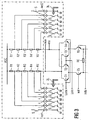
- the first Current source SI1 and the second current source SI2 through a resistance current source network were replaced.
- the resistance power source network serves as position SE.
- To five resistors R1 to R5 are connected in series.
- the Free connection of resistor R1 is with a supply potential VCC connected.
- the free connection of the resistor R5 is with both the mixer output mox and the collector of a transistor T1 and the collector of a transistor T3, which are components of the mixer MI, connected.
- the resistors R1 to R5 are each one Current source that delivers a constant current i and over each a switch that connects to the appropriate power source is connected in series with the reference potential M.
- the current sources that each supply the current i are with a current source that impresses a reference current iref1, coupled.
- the path for the inverted signal is symmetrical to the path for the in-phase signal just described built up.
- the resistors in the path for the inverted signal are denoted by R1 'to R5'.
- the reference current source delivers the reference current iref2, which is equal to the first reference current can be iref1.
- the resistor R5 ' is with the Output mo of the mixer MI, the collector of a second transistor T2 and the collector of a fourth transistor T4 connected, which are also part of the mixer MI.
- the two transistors T1 and T2 and the two transistors T3 and T4 emitter-coupled and each with the collector of a fifth or a sixth transistor T5 or T6 connected.
- the base connection of the fifth Transistor T5 is with the input inif, the base connection of the sixth transistor T6 with the input inifx, the base connection of the first transistor T1 with the input loinx and the base terminal of the fourth transistor T4 and the Base terminal of the third transistor T3 is connected to the input loinx and the base terminal of the second transistor T2 connected.
- the collectors of the transistors T1 and T3 and the collectors of the transistors T2 and T4 with each other connected.
- a resistor RE is connected between the emitters of transistors T5 and T6 a resistor RE is connected.
- the basic connection of transistor T5 is with the input inif and the base terminal of transistor T6 is connected to the inifx input.
- the letter "x" denotes the inverted connection.
- the comprising the transistors T1 to T6 and the resistor RE Mixer MI according to FIG. 3 represents only one possible one Embodiment of a mixer. Others can Mixer circuits are used instead of those just described become.
- the switches S are controlled via the 3-wire bus 3L, and thereby the desired current or the desired Voltage for offset compensation set.
- resistors R1 'to R5' The dimensioning and the resistance ratios between R1 and R2 up to R5 are depending on the application to the respective circumstances adapt.
- the embodiment according to FIG. 3 has the additional advantage that the resistance power source network is even easier is to be produced as the actuator (SE) according to the arrangement Figure 2.
- the working resistances of the mixer MI are shown in FIG. 3 in several individual resistors R1 to R5 connected in series or R1 'to R5' divided.
- the embodiment shown in Figure 3 the compensation of Offset voltage only once, the first time Commissioning. This is not the case with applied signals the offset voltage in the downstream Baseband IC2 measured and depending on the size of the Offset voltages become the corresponding ones via the 3-wire bus 3L Power sources activated via the switches S.
- the offset correction value is advantageously stored in a ROM of the baseband module IC2. With every new start-up of the device is loaded when the 3-wire bus 3L offset compensation is carried out automatically. Is to only read the value from the ROM and the corresponding Power sources must be activated.
- the detection of the offset of the mixer MI can by the im Baseband module IC2 already existing analog-digital converter respectively. This has the advantage that no additional Circuit elements for detecting the offset of the mixer are needed.
Landscapes
- Engineering & Computer Science (AREA)
- Power Engineering (AREA)
- Amplifiers (AREA)
Description
- Figur 1
- zeigt die Kompensation des Offsets gemäß dem Stand der Technik.
- Figur 2
- zeigt eine erste erfindungsgemäße Ausführungsform der Anordnung zur Kompensation des Offsets eines Mischers.
- Figur 3
- zeigt eine zweite erfindungsgemäße Ausführungsform der Anordnung zur Kompensation des Offsets eines Mischers.
Claims (9)
- Anordnung zur Kompensation des Offsets eines Mischers,bei der ein erster integrierter Schaltkreis (IC1) vorgesehen ist, der den Mischer (M) und eine Stelleinheit (SE) zur Erzeugung'eines Offsetkompensationswerts aufweist, welche mit dem Mischer (MI) verbunden ist,bei der ein Bus (3L) vorgesehen ist,bei der ein zweiter integrierter Schaltkreis (IC2) vorgesehen ist, der ein Mittel zur Erfassung (E) des Offsets des Mischers (MI) aufweist und den erfassten Offset auf den Bus (3L) ausgibt,bei der der Offset über den Bus (3L) der Stelleinheit (SE) zugeführt wird.
- Anordnung nach Anspruch 1,
bei der die Stelleinheit (SE) eine oder mehrere einstellbare Stromquellen (I1, I2) aufweist. - Anordnung nach Anspruch 2,
bei der die einstellbare Stromquelle (SI1, SI2) mehrere zuschaltbare parallel zueinander geschaltete Konstantstromquellen (i, 2i, 4i, 8i) aufweist. - Anordnung nach Anspruch 1,
bei der die Stelleinheit (SE) mehrere in Reihe geschaltete Widerstände (R1, R3, R4, R5, R6) und mehrere zuschaltbare Stromquellen (i) aufweist, die mit den Widerständen (R1, R3, R4, R5, R6) derart verbunden sind, daß verschiedene Spannungen einstellbar sind. - Anordnung nach einem der Ansprüche 1 bis 4,
bei der ein Speicher vorgesehen ist, in den der Offsetkompensationswert geschrieben wird. - Anordnung nach Anspruch 5,
bei der der Speicher ein nichtflüchtiges Element ist. - Anordnung nach einem der Ansprüche 1 bis 6,
bei der der Bus (3L) ein 3-Leiter-Bus ist. - Verfahren zur Kompensation des Offsets eines Mischers,bei dem der Mischer (MI), welcher Bestandteil eines ersten integrierten Schaltkreises (IC1) ist, ohne Eingangssignal betrieben wird und der Offset des Ausgangssignals das Mischers (MI) mit einem Mittel zur Erfassung (E) des Offsets des Mischers (MI), welches Bestandteil eines zweiten integrierten Schaltkreises (IC2) ist, erfasst wird,bei dem der erfasste Offset über einen Bus (3L) an eine Stelleinheit (SE), welche Bestandteil des ersten integrierten Schaltkreises (IC1) ist, übermittelt wird,bei dem die Stelleinheit (SE) einen entsprechenden Offsetkompensationswert dem Mischer (MI) zuführt.
- Verfahren nach Anspruch 8,bei dem der erfasste Offset in einen nichtflüchtigen Speicher geschrieben wird,bei dem der im Speicher stehende Offset bei einer Inbetriebnahme des ersten integrierten Schaltkreises (IC1) ausgelesen wird und über den Bus (3L) der Stelleinheit (SE). zur Verfügung gestellt wird.
Applications Claiming Priority (2)
| Application Number | Priority Date | Filing Date | Title |
|---|---|---|---|
| DE19743272A DE19743272C1 (de) | 1997-09-30 | 1997-09-30 | Anordnung und Verfahren zur Kompensation des Offsets eines Mischers |
| DE19743272 | 1997-09-30 |
Publications (2)
| Publication Number | Publication Date |
|---|---|
| EP0905880A1 EP0905880A1 (de) | 1999-03-31 |
| EP0905880B1 true EP0905880B1 (de) | 2003-11-19 |
Family
ID=7844201
Family Applications (1)
| Application Number | Title | Priority Date | Filing Date |
|---|---|---|---|
| EP98116859A Expired - Lifetime EP0905880B1 (de) | 1997-09-30 | 1998-09-07 | Anordnung und Verfahren zur Kompensation des Offsets eines Mischers |
Country Status (2)
| Country | Link |
|---|---|
| EP (1) | EP0905880B1 (de) |
| DE (2) | DE19743272C1 (de) |
Families Citing this family (5)
| Publication number | Priority date | Publication date | Assignee | Title |
|---|---|---|---|---|
| DE19904376A1 (de) * | 1999-02-03 | 2000-08-17 | Siemens Ag | Verfahren und Schaltung zur Kompensationssteuerung von Offsetspannungen einer in einem Schaltungsbaustein integrierten Funkempfangsschaltung |
| NO329890B1 (no) * | 1999-11-15 | 2011-01-17 | Hitachi Ltd | Mobilkommunikasjonsapparat |
| EP1134889A1 (de) | 2000-03-13 | 2001-09-19 | Infineon Technologies AG | Anordnung und Verfahren zur Kompensation des Eingangs-Offsets eines Mischers |
| FR2847744A1 (fr) * | 2002-11-26 | 2004-05-28 | St Microelectronics Sa | Procede de reduction de la non-linearite d'ordre deux d'un dispositif de transposition de frequence et dispositif correspondant |
| US8693961B2 (en) | 2011-08-11 | 2014-04-08 | Intel IP Corporation | System and method for improving power efficiency of a transmitter |
Family Cites Families (5)
| Publication number | Priority date | Publication date | Assignee | Title |
|---|---|---|---|---|
| US4717888A (en) * | 1986-05-22 | 1988-01-05 | Raytheon Company | Integrated circuit offset voltage adjustment |
| US4827222A (en) * | 1987-12-11 | 1989-05-02 | Vtc Incorporated | Input offset voltage trimming network and method |
| US4987327A (en) * | 1989-05-30 | 1991-01-22 | Motorola, Inc. | Apparatus for adjusting DC offset voltage |
| EP0693823B1 (de) * | 1994-07-18 | 2001-04-18 | Infineon Technologies AG | Schaltungsanordnung, insbesondere für digitale Modulationseinrichtungen |
| US5471665A (en) * | 1994-10-18 | 1995-11-28 | Motorola, Inc. | Differential DC offset compensation circuit |
-
1997
- 1997-09-30 DE DE19743272A patent/DE19743272C1/de not_active Expired - Fee Related
-
1998
- 1998-09-07 EP EP98116859A patent/EP0905880B1/de not_active Expired - Lifetime
- 1998-09-07 DE DE59810211T patent/DE59810211D1/de not_active Expired - Lifetime
Also Published As
| Publication number | Publication date |
|---|---|
| EP0905880A1 (de) | 1999-03-31 |
| DE59810211D1 (de) | 2003-12-24 |
| DE19743272C1 (de) | 1999-02-18 |
Similar Documents
| Publication | Publication Date | Title |
|---|---|---|
| DE69522447T2 (de) | Puls-zähl-fm-demodulator und empfänger damit | |
| DE69431905T2 (de) | Leitungstreiber mit adaptiver ausgangsimpedanz | |
| DE69413365T2 (de) | Verstärker mit einstellbarer Verstärkung | |
| DE3725339A1 (de) | Automatische justierschaltung zum justieren der zeitkonstanten einer filterschaltung | |
| DE69102940T2 (de) | Kapazitiver Positionsdetektor. | |
| EP1154565A2 (de) | Verstärkerschaltung mit Offset-Kompensation, inbesondere für digitale Modulationseinrichtungen | |
| DE69226862T2 (de) | Frequenzabstimmungssystem für ein Paar C-Transkonduktanzoperationsverstärker | |
| DE19945709C2 (de) | Schaltungsanordnung zur Regelung des Arbeitspunkts eines Leistungsverstärkers und deren Verwendung | |
| DE69406843T2 (de) | Vierquadranten-Multiplizierschaltung und eine solche Schaltung enthaltender Empfänger | |
| DE69611749T2 (de) | Verstärkerschaltung mit variabler Verstärkung | |
| DE3406150A1 (de) | Steuerschaltung zum abstimmen an einer hochfrequenz-eingangsschaltung | |
| DE3319292C2 (de) | Schaltungsanordnung zur Rauschverminderung | |
| DE19743272C1 (de) | Anordnung und Verfahren zur Kompensation des Offsets eines Mischers | |
| DE3788413T2 (de) | Filterschaltung. | |
| DE2433298C3 (de) | Resonanzkreis, gebildet aus einem Gyrator | |
| DE69023694T2 (de) | Gleichstromsperrender Verstärker. | |
| DE60037569T2 (de) | Vorrichtung und verfahren zur umsetzung von spannung in strom | |
| DE69421260T2 (de) | Spannungsgesteuerte Kapazität | |
| EP0133618B1 (de) | Monolithisch integrierte Transistor-Hochfreqzenz-Quarzoszillatorschaltung | |
| DE2855168C2 (de) | Bipolarer Spannungsdetektor | |
| DE69721898T2 (de) | Verstärker mit variabler Verstärkung und geringer Gleichspannungsabweichung am Ausgang und geringen Verzerrungen | |
| DE2646737B2 (de) | Hilfstraeger-regenerationsschaltung fuer einen farbfernsehempfaenger | |
| EP0363626B1 (de) | Schaltungsanordnung zur Pegelumsetzung digitaler Signale | |
| DE3127889C2 (de) | Schaltungsanordnung aus mindestens zwei Verstärkern | |
| EP0309451B1 (de) | Schutzvorrichtung gegen störsignale |
Legal Events
| Date | Code | Title | Description |
|---|---|---|---|
| PUAI | Public reference made under article 153(3) epc to a published international application that has entered the european phase |
Free format text: ORIGINAL CODE: 0009012 |
|
| AK | Designated contracting states |
Kind code of ref document: A1 Designated state(s): DE FI FR GB SE |
|
| AX | Request for extension of the european patent |
Free format text: AL;LT;LV;MK;RO;SI |
|
| 17P | Request for examination filed |
Effective date: 19990419 |
|
| AKX | Designation fees paid |
Free format text: DE FI FR GB SE |
|
| RAP1 | Party data changed (applicant data changed or rights of an application transferred) |
Owner name: INFINEON TECHNOLOGIES AG |
|
| GRAH | Despatch of communication of intention to grant a patent |
Free format text: ORIGINAL CODE: EPIDOS IGRA |
|
| GRAH | Despatch of communication of intention to grant a patent |
Free format text: ORIGINAL CODE: EPIDOS IGRA |
|
| GRAA | (expected) grant |
Free format text: ORIGINAL CODE: 0009210 |
|
| AK | Designated contracting states |
Kind code of ref document: B1 Designated state(s): DE FI FR GB SE |
|
| REG | Reference to a national code |
Ref country code: GB Ref legal event code: FG4D Free format text: NOT ENGLISH |
|
| REF | Corresponds to: |
Ref document number: 59810211 Country of ref document: DE Date of ref document: 20031224 Kind code of ref document: P |
|
| REG | Reference to a national code |
Ref country code: SE Ref legal event code: TRGR |
|
| GBT | Gb: translation of ep patent filed (gb section 77(6)(a)/1977) |
Effective date: 20040209 |
|
| ET | Fr: translation filed | ||
| PG25 | Lapsed in a contracting state [announced via postgrant information from national office to epo] |
Ref country code: FI Free format text: LAPSE BECAUSE OF NON-PAYMENT OF DUE FEES Effective date: 20040907 |
|
| PG25 | Lapsed in a contracting state [announced via postgrant information from national office to epo] |
Ref country code: SE Free format text: LAPSE BECAUSE OF NON-PAYMENT OF DUE FEES Effective date: 20040908 |
|
| PLBE | No opposition filed within time limit |
Free format text: ORIGINAL CODE: 0009261 |
|
| STAA | Information on the status of an ep patent application or granted ep patent |
Free format text: STATUS: NO OPPOSITION FILED WITHIN TIME LIMIT |
|
| 26N | No opposition filed |
Effective date: 20040820 |
|
| EUG | Se: european patent has lapsed | ||
| REG | Reference to a national code |
Ref country code: FR Ref legal event code: TP Owner name: INTEL MOBILE COMMUNICATIONS GMBH, DE Effective date: 20120404 Ref country code: FR Ref legal event code: CA Effective date: 20120404 |
|
| REG | Reference to a national code |
Ref country code: GB Ref legal event code: 732E Free format text: REGISTERED BETWEEN 20120607 AND 20120613 |
|
| REG | Reference to a national code |
Ref country code: GB Ref legal event code: 732E Free format text: REGISTERED BETWEEN 20121213 AND 20121219 |
|
| REG | Reference to a national code |
Ref country code: DE Ref legal event code: R081 Ref document number: 59810211 Country of ref document: DE Owner name: INTEL MOBILE COMMUNICATIONS GMBH, DE Free format text: FORMER OWNER: INTEL MOBILE COMMUNICATIONS GMBH, 85579 NEUBIBERG, DE Effective date: 20130315 Ref country code: DE Ref legal event code: R081 Ref document number: 59810211 Country of ref document: DE Owner name: INTEL MOBILE COMMUNICATIONS GMBH, DE Free format text: FORMER OWNER: INFINEON TECHNOLOGIES AG, 81669 MUENCHEN, DE Effective date: 20130314 Ref country code: DE Ref legal event code: R081 Ref document number: 59810211 Country of ref document: DE Owner name: INTEL MOBILE COMMUNICATIONS GMBH, DE Free format text: FORMER OWNER: INTEL MOBILE COMMUNICATIONS TECHNOLOGY GMBH, 85579 NEUBIBERG, DE Effective date: 20130326 Ref country code: DE Ref legal event code: R081 Ref document number: 59810211 Country of ref document: DE Owner name: INTEL MOBILE COMMUNICATIONS GMBH, DE Free format text: FORMER OWNER: INFINEON TECHNOLOGIES AG, 85579 NEUBIBERG, DE Effective date: 20130315 |
|
| PGFP | Annual fee paid to national office [announced via postgrant information from national office to epo] |
Ref country code: GB Payment date: 20140903 Year of fee payment: 17 |
|
| PGFP | Annual fee paid to national office [announced via postgrant information from national office to epo] |
Ref country code: FR Payment date: 20140906 Year of fee payment: 17 |
|
| PGFP | Annual fee paid to national office [announced via postgrant information from national office to epo] |
Ref country code: DE Payment date: 20150902 Year of fee payment: 18 |
|
| REG | Reference to a national code |
Ref country code: FR Ref legal event code: CD Owner name: INTEL DEUTSCHLAND GMBH, DE Effective date: 20160126 |
|
| GBPC | Gb: european patent ceased through non-payment of renewal fee |
Effective date: 20150907 |
|
| REG | Reference to a national code |
Ref country code: FR Ref legal event code: ST Effective date: 20160531 |
|
| PG25 | Lapsed in a contracting state [announced via postgrant information from national office to epo] |
Ref country code: GB Free format text: LAPSE BECAUSE OF NON-PAYMENT OF DUE FEES Effective date: 20150907 |
|
| PG25 | Lapsed in a contracting state [announced via postgrant information from national office to epo] |
Ref country code: FR Free format text: LAPSE BECAUSE OF NON-PAYMENT OF DUE FEES Effective date: 20150930 |
|
| REG | Reference to a national code |
Ref country code: DE Ref legal event code: R119 Ref document number: 59810211 Country of ref document: DE |
|
| PG25 | Lapsed in a contracting state [announced via postgrant information from national office to epo] |
Ref country code: DE Free format text: LAPSE BECAUSE OF NON-PAYMENT OF DUE FEES Effective date: 20170401 |