EP0905847A2 - Fehlerstrom-Schutzeinrichtung - Google Patents
Fehlerstrom-Schutzeinrichtung Download PDFInfo
- Publication number
- EP0905847A2 EP0905847A2 EP98117740A EP98117740A EP0905847A2 EP 0905847 A2 EP0905847 A2 EP 0905847A2 EP 98117740 A EP98117740 A EP 98117740A EP 98117740 A EP98117740 A EP 98117740A EP 0905847 A2 EP0905847 A2 EP 0905847A2
- Authority
- EP
- European Patent Office
- Prior art keywords
- residual current
- comparator
- led2
- led3
- led1
- Prior art date
- Legal status (The legal status is an assumption and is not a legal conclusion. Google has not performed a legal analysis and makes no representation as to the accuracy of the status listed.)
- Granted
Links
Images


Classifications
-
- H—ELECTRICITY
- H02—GENERATION; CONVERSION OR DISTRIBUTION OF ELECTRIC POWER
- H02H—EMERGENCY PROTECTIVE CIRCUIT ARRANGEMENTS
- H02H3/00—Emergency protective circuit arrangements for automatic disconnection directly responsive to an undesired change from normal electric working condition with or without subsequent reconnection ; integrated protection
- H02H3/02—Details
- H02H3/04—Details with warning or supervision in addition to disconnection, e.g. for indicating that protective apparatus has functioned
-
- H—ELECTRICITY
- H02—GENERATION; CONVERSION OR DISTRIBUTION OF ELECTRIC POWER
- H02H—EMERGENCY PROTECTIVE CIRCUIT ARRANGEMENTS
- H02H3/00—Emergency protective circuit arrangements for automatic disconnection directly responsive to an undesired change from normal electric working condition with or without subsequent reconnection ; integrated protection
- H02H3/26—Emergency protective circuit arrangements for automatic disconnection directly responsive to an undesired change from normal electric working condition with or without subsequent reconnection ; integrated protection responsive to difference between voltages or between currents; responsive to phase angle between voltages or between currents
- H02H3/32—Emergency protective circuit arrangements for automatic disconnection directly responsive to an undesired change from normal electric working condition with or without subsequent reconnection ; integrated protection responsive to difference between voltages or between currents; responsive to phase angle between voltages or between currents involving comparison of the voltage or current values at corresponding points in different conductors of a single system, e.g. of currents in go and return conductors
- H02H3/33—Emergency protective circuit arrangements for automatic disconnection directly responsive to an undesired change from normal electric working condition with or without subsequent reconnection ; integrated protection responsive to difference between voltages or between currents; responsive to phase angle between voltages or between currents involving comparison of the voltage or current values at corresponding points in different conductors of a single system, e.g. of currents in go and return conductors using summation current transformers
Definitions
- the invention relates to a residual current device.
- a residual current device serves to ensure protection against a dangerous fault current in a electrical system.
- a fault current or operational Working current occurs when a live part an electrical system against electrical contact Earth. This is the case, for example, if a person a live part of an electrical System touches. The fault current then flows over the person as body current against earth.
- the protection against dangerous Body currents used residual current protective devices must then with a fault current that is greater than that Rated residual current is safe and fast electrical Disconnect the system from the mains.
- a residual current device is for example from etz ", volume 107 (1986), number 20, pages 938 to 945.
- As a residual current circuit breaker or FI Circuit breaker is a residual current device in which the electrical energy required for tripping is obtained independently of the mains voltage from the fault current itself.
- the so-called residual current or DI circuit breaker is a residual current device in which the electrical required for tripping
- Such a DI circuit breaker therefore requires a mains connection and a power supply unit for its operation, which converts the mains voltage into the supply voltage required to operate its components.
- the invention is based on the object, a residual current device to indicate with which it is possible the occurrence of a fault current in an electrical system independent of the triggering of a disconnector.
- the residual current protective device contains a detection device for detection of a fault current and a comparison device for Comparing the fault current with at least one predetermined one Reference value and for driving at least one optical Residual current display element.
- the optical residual current display element enables a statement about the operating state of an electrical system with regard to of a fault current occurring in it. So can with the help of a single optical fault current display element displayed whether a fault current occurs in the system, which, for example, is not yet triggering one Circuit breaker causes, but still signals that in a fault current is already flowing in the electrical system Causes must be checked in order to switch off the electrical system at an unfavorable time.
- Another advantage is that with a residual current device with adjustable rated or Nominal residual current whose setting, i.e. Adaptation to the Operating conditions of the protected system is facilitated.
- This rated residual current must be greater than the operational one Leakage current, i.e. be larger than that in normal operation fault current flowing in the electrical system.
- One too low set rated fault current leads to an undesired Switch off.
- the rated residual current can then successively set to a value at which the Reference value supplied to the comparison device is not reached will, i.e. the optical residual current indicator goes out or starts to glow.
- the detection device contains the detection device generates an electrical circuit a fault voltage derived from the fault current.
- those detected by the detection device can be Signals in downstream electronic components simply processed further.
- the comparison device preferably contains one designed as a Schmitt trigger circuit comparator circuit to compare the error voltage with a reference voltage.
- the comparator circuit contains for each optical Residual current display element a particularly as Schmitt trigger trained comparator, especially one CMOS comparator.
- This measure is for the optical Indication of the required power consumption of the residual current protective device decreased.
- This power consumption would with a typical power supply with a supply of three Outer conductors (3-phase AC system), one B6 bridge rectifier circuit and a simple series regulator at an outer conductor voltage of 480V about 0.66W per 1mA current consumption. At 480V line voltage at the output of the B6 bridge rectifier circuit about 670V DC voltage on.
- the series regulator which in principle is a in line to the consumer, i.e.
- the residual current protective device is used to check the function at least one optical operating display element provided that preferably without intermediary a comparator is connected to a power supply.
- light emitting diodes are used as optical display elements intended. This further reduces the power consumption.
- a pulse generator for operating the at least one optical Display element provided in pulse mode. This enables a further reduction in power consumption.
- optical fault current display elements between the comparator circuit and the pulse generator and the optical power indicator between the power supply and switched the pulse generator.
- the relationship between light pause and light duration at Pulse operation of the optical display element is at least 5. In this way, the power consumption can be significantly reduced become.
- the pulse generator also contains a discrete comparator, especially a CMOS comparator.
- the optical Display elements switched in parallel. Thereby is the same brightness by simple wiring all optical display elements possible.
- optical display elements are connected in series. Thereby can the power consumption in the event that all display elements shine, be minimized.
- each comparator is as push pull "output switched.
- the output of each comparator of the comparator circuit is as open drain "output. This means that the number of components and thus also the current consumption can be reduced when the optical display elements are connected in series.
- a residual current protective device comprises a Detection device 4, with which one in a network L1, L2, L3, N flowing fault current can be detected.
- the fault current this is done in a summation current transformer such as that used for example is shown in the technical article mentioned at the beginning and in the detection device 4 into a voltage signal converted.
- This voltage signal is in an amplifier 6 amplified and as error voltage UE to a comparison device 8 forwarded.
- the comparison device 8 comprises a comparator circuit 10 in which the error voltage UE with at least one reference voltage Uref is compared to that of the comparator circuit 10 provided by a reference circuit 12 becomes.
- the output of the comparator circuit 10 is an optical one Display device 14 connected, which is an optical operating display element, in the example a light emitting diode LED1, as well two optical fault current display elements, in the example Light emitting diodes LED2, LED3.
- a power supply unit 20 is provided, which is provided by the network 3-phase AC voltage in one for operating the residual current protective device 2 required DC voltage U converts.
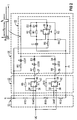
- the three light emitting diodes are LED1, LED2 and LED3 the display device 14, in particular light-emitting diodes with less Power consumption and high luminosity, parallel to each other switched and to the output of a pulse generator 22nd connected.
- the pulse generator 22 is suitable from one connected comparator V1, preferably a CMOS comparator, built up.
- the pulse generator 22 which corresponds to the output 26 of the comparator V1
- there is a pulsed voltage which pulsates between 0 V and the comparator output voltage U V , which is approximately equal to the operating voltage U.
- the time duration t H of the voltage pulse, ie voltage level HIGH "(light pause), and the time period t L between two successive voltage pulses, ie voltage level LOW “(lighting time) can be set by suitable dimensioning of the external circuitry of the comparator V1.
- the output 26 of the comparator V1 is connected to ground via a series connection of a diode D1, a charging resistor R1 and a capacitor C.
- the LED1 serving as an operating display element is connected with its cathode directly to the output 24 of the pulse generator 22 and with its anode to the supply voltage U via a series resistor R6.
- the comparator output voltage U V is present at the output 24 of the pulse generator 22
- no current can flow via the light-emitting diode LED1, so that it does not light up.
- the duration of a lighting pause thus corresponds to the duration t H of the voltage pulse generated by the function generator 22. If the output 24 of the pulse generator 22 is at 0 V, a current can flow to ground via the light-emitting diode LED1 and the comparator V1 and the light-emitting diode LED1 lights up.
- the lighting duration thus corresponds to the time duration t L between two successive voltage pulses.
- the capacitance of the capacitor C is preferably more than 100 nF, in the exemplary embodiment 470 nf.
- the resistors R1 and R2 are dimensioned as low as possible. This ensures the function of the pulse generator regardless of the reverse current of diodes D1 and D2 at temperatures of ⁇ 70 ° C.
- the resistors R3, R4, R5 are high-resistance and are used to generate the reference voltage at input 26 of comparator V1.
- the comparator V1 via separate inputs to the supply voltage U and Ground is connected.
- the first fault current display element Light-emitting diode LED2 and a further fault current display element provided light emitting diode LED3 are each via a Protection diode D4 or D3 also at the output 24 of the pulse generator 22 connected.
- the anodes of the light emitting diodes LED2 and LED3 are each via a series resistor R8 or R7 connected to the outputs 26, 27 of the comparator circuit 10.
- the comparator circuit 10 contains two comparators V2, V3, which are identical in the preferred embodiment with the comparator V1.
- the comparator V2 is with one Input 30 to the fault voltage derived from the fault current UE connected.
- a reference voltage Uref1 applied by the Comparator V2 is compared with the error voltage UE.
- a Feedback resistor R10 is used to implement the Schmitt trigger function of the comparator V2.
- the output voltage U V ⁇ U is present at the output 28 of the comparator V2 and thus also at the output 26 of the comparator circuit 10, so that when the voltage 0 is present at the output 24 of the pulse generator 22, a current flows through the LED2.
- the protective diode D4 is provided to protect the light-emitting diode LED2 when the voltage 0 is present at the output 28 of the comparator V2 and the operating voltage U, for example 12V, is present at the output 24 of the pulse generator 22, since the maximum permissible reverse voltage for light-emitting diodes is generally lower than is the operating voltage U required to operate the residual current device.
- the LED2 therefore flashes when the error voltage UE is greater than the reference voltage Uref1 set via the resistors R10, R11 and R12. In contrast, the light-emitting diode LED1 flashes regardless of the value of the error voltage UE in the duty cycle impressed by the pulse generator 22.
- a second reference voltage Uref2 becomes the reference input 34 of the further comparator V3, the output 36 connected to the output 27 of the comparator circuit 10 is.
- the series resistor R7 Anode of the serving as a further fault current display element LED3 connected.
- the cathode of the light emitting diode LED3 is connected to the output 24 of the pulse generator via a protective diode D3 22 switched.
- the fault voltage UE is usually based on the nominal or rated fault current standardized. In other words: the amount the fault voltage UE only depends on the ratio between the rated fault current and the actual fault current. With a residual current device, this also enables adjustable rated fault current a simple setting of the rated residual current to the operating conditions of the electrical system. The rated residual current can then be at proper operation of the plant based on a high Output value (LED2 and LED3 do not flash) successively reduced become. A setting with the LED2 just yet not lit, then corresponds to a rated residual current, that according to the above embodiment approximately four times of the operational leakage current. In this way can easily set the residual current protective device and false trips are avoided.
- the resistors R6, R7 and R8 must be dimensioned larger than 1k ⁇ each.
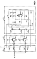
- the light-emitting diodes LED1, LED2, LED3 are connected in series with one another.
- the output 24 of the pulse generator 22 is connected to the anode of the light-emitting diode LED1 via the series resistor R6.
- the comparator V2 provides at its output 28, depending on whether the error voltage UE is smaller or larger than the reference voltage Uref1, the voltage 0 or the voltage U V ⁇ U.
- the protective diode D4 is polarized in the forward direction and a current flows through the light-emitting diode LED1, the protective diode D4, the resistor R7 and the comparator V2 in accordance with the pulse duty factor of the pulse generator 22. If the error voltage UE exceeds the reference voltage Uref1, the protective diode D4 is operated in the reverse direction and the current flowing from the comparator V1 via resistor R6 and LED LED1 flows through the LED LED2, the protective diode D3 from the series resistor R13 and the comparator V3.
- the two protective diodes D3 and D4 are operated in the reverse direction and current flows through all three light-emitting diodes LED1, LED2, LED3, so that they flash in accordance with the pulse duty factor of the pulse generator 22.
- the comparators V1, V2 and V3 are so-called in the exemplary embodiments according to FIGS. 2 and 3 Push-pull "output operated. In this mode of operation there are always defined voltage values U V , in the exemplary embodiment approximately the operating voltage U, or ground potential at the outputs 26, 28 and 36 of the comparators V1, V2, V3.
- CMOS comparators with a particularly low current consumption that are connected or designed as Schmitt triggers are suitable as comparators.
- comparators V2, V3 designed as Schmitt triggers an instability of the display caused by the inevitable ripple of the error voltage can be avoided.
- the resistors R13 and R14 enable a reduction in the drop in the current flowing through the light-emitting diodes LED1, LED2, LED3 when the light-emitting diode LED2 and light-emitting diode LED3 are switched on. If only the LED1 flashes, the current flowing through it is I.
- the output 26 of the comparator V1 of the pulse generator 22 is connected to the supply voltage U via a resistor R14 in order to be able to assume a defined output state.
- a resistor R14 When wiring with such an external circuit is necessary to ensure defined voltage conditions at the output of a comparator V1.
- LED (U V -U LED1 -U LED2 -U LED3 ) / R6 (U LED2 , U LED3 : voltage drop at LED2 or LED3).
- U 12V ⁇ U V
- the advantage of this circuit lies essentially in the saving of the protective diodes D3 and D4 and in the reduced current consumption due to the series connection of the light-emitting diodes LED1, LED2, LED3. If a brightness compensation of the light-emitting diodes LED1, LED2, LED3 is required, this can be effected by adding resistors R13 and R14 analogously to the exemplary embodiment according to FIG. 3.
Landscapes
- Emergency Protection Circuit Devices (AREA)
- Control Of Indicators Other Than Cathode Ray Tubes (AREA)
- Electronic Switches (AREA)
- Protection Of Static Devices (AREA)
- Circuit Arrangement For Electric Light Sources In General (AREA)
Abstract
Description
- FIG 1
- eine Fehlerstrom-Schutzeinrichtung gemäß der Erfindung in einer Prinzipdarstellung,
- FIG 2
- eine Fehlerstrom-Schutzeinrichtung mit drei parallel zueinander geschalteten optischen Anzeigeelementen,
- FIG 3 und 4
- jeweils eine Fehlerstrom-Schutzeinrichtung mit drei in Reihe geschalteten optischen Anzeigeelementen.
Die Widerstände R13 und R14 ermöglichen eine Reduzierung des Abfalles des über die Leuchtdioden LED1,LED2,LED3 fließenden Stromes bei Zuschaltung von Leuchtdiode LED2 und Leuchtdiode LED3. Blinkt nur die Leuchtdiode LED1, beträgt der über sie fließende Strom
Claims (20)
- Fehlerstrom-Schutzeinrichtung, mit einer Detektionseinrichtung (4) zum Erfassen eines Fehlerstromes, und mit einer Vergleichseinrichtung (8) zum Vergleichen des Fehlerstromes mit wenigstens einem vorgegebenen Referenzwert und zum Ansteuern zumindest eines optischen Fehlerstrom-Anzeigeelementes (LED2,LED3).
- Fehlerstrom-Schutzeinrichtung nach Anspruch 1, bei der die Detektionseinrichtung (4) eine Schaltung zum Erzeugen einer aus dem Fehlerstrom abgeleiteten Fehlerspannung (UE) enthält.
- Fehlerstrom-Schutzeinrichtung nach Anspruch 2, bei der die Vergleichseinrichtung (8) eine Komparatorschaltung (10) zum Vergleichen der Fehlerspannung (UE) mit einer Referenzspannung (Uref1,Uref2) umfaßt.
- Fehlerstrom-Schutzeinrichtung nach Anspruch 3, bei der die Komparatorschaltung (10) als Schmitt-Trigger-Schaltung ausgebildet ist.
- Fehlerstrom-Schutzeinrichtung nach Anspruch 3 oder 4, bei der die Komparatorschaltung (10) für jedes optische Fehlerstrom-Anzeigeelement (LED2,LED3) einen Komparator (V2,V3) enthält.
- Fehlerstrom-Schutzeinrichtung nach Anspruch 5, bei der der Komparator (V2,V3) als Schmitt-Trigger ausgebildet ist.
- Fehlerstrom-Schutzeinrichtung nach einem der vorhergehenden Ansprüche, bei der zu ihrer Funktionskontrolle zumindest ein optisches Betriebs-Anzeigeelement (LED1) vorgesehen ist.
- Fehlerstrom-Schutzeinrichtung nach Anspruch 7, bei der das optische Betriebs-Anzeigeelement (LED1) ohne Zwischenschaltung eines Komparators an ein Netzteil (20) angeschlossen ist.
- Fehlerstrom-Schutzeinrichtung nach Anspruch 7 oder 8, bei der als optisches Betriebs-Anzeigeelement (LED1) eine Leuchtdiode vorgesehen ist.
- Fehlerstrom-Schutzeinrichtung nach einem der vorhergehenden Ansprüche, bei der als optisches Fehler-Anzeigeelement (LED2,LED3) eine Leuchtdiode vorgesehen ist.
- Fehlerstrom-Schutzeinrichtung nach einem der vorhergehenden Ansprüche, mit einem Impulsgenerator (22) zum Betreiben zumindest eines optischen Anzeigeelementes (LED1,LED2, LED3) im Pulsbetrieb.
- Fehlerstrom-Schutzeinrichtung nach Anspruch 11, bei dem die optischen Fehlerstrom-Anzeigeelemente (LED2,LED3) zwischen einem Ausgang (24) des lmpulsgenerators (22) und einem Ausgang (26,27) der Komparatorschaltung (10) geschaltet sind.
- Fehlerstrom-Schutzeinrichtung nach Anspruch 11, bei dem das Betriebs-Anzeigeelement (LED1) zwischen einem Ausgang (24) des Impulsgenerators (22) und das Netzteil (20) geschaltet sind.
- Fehlerstrom-Schutzeinrichtung nach einem der Ansprüche 11 bis 13, bei der das Verhältnis zwischen Leuchtpause (tH) und Leuchtdauer (tL) beim Pulsbetrieb des optischen Anzeigeelementes (LED1,LED2, LED3) wenigstens 5 beträgt.
- Fehlerstrom-Schutzeinrichtung nach einem der Ansprüche 11 bis 14, bei der der Impulsgenerator (22) einen Komparator (V1) enthält.
- Fehlerstrom-Schutzeinrichtung nach einem der Ansprüche 5 bis 15, bei der jeder Komparator (V1,V2,V3) ein CMOS-Komparator ist.
- Fehlerstrom-Schutzeinrichtung nach einem der vorhergehenden Ansprüche, mit einer Mehrzahl von optischen Anzeigeelementen (LED1,LED2,LED3), die parallel zueinander geschaltet sind.
- Fehlerstrom-Schutzeinrichtung nach einem der vorhergehenden Ansprüche, mit einer Mehrzahl von optischen Anzeigeelementen (LED1,LED2,LED3), die in Reihe geschaltet sind.
- Fehlerstrom-Schutzeinrichtung nach einem der Ansprüche 16 bis 18, bei der der Ausgang (24,28,34) jedes Komparators (V1,V2,V3) alspush pull"-Ausgang geschaltet ist.

- Fehlerstrom-Schutzeinrichtung nach einem der Ansprüche 16 bis 18, bei der der Ausgang (28,34) jedes Komparators (V2,V3) der Komparatorschaltung (10) als
Applications Claiming Priority (2)
| Application Number | Priority Date | Filing Date | Title |
|---|---|---|---|
| DE19743036 | 1997-09-30 | ||
| DE19743036 | 1997-09-30 |
Publications (3)
| Publication Number | Publication Date |
|---|---|
| EP0905847A2 true EP0905847A2 (de) | 1999-03-31 |
| EP0905847A3 EP0905847A3 (de) | 2001-03-14 |
| EP0905847B1 EP0905847B1 (de) | 2003-05-02 |
Family
ID=7844029
Family Applications (1)
| Application Number | Title | Priority Date | Filing Date |
|---|---|---|---|
| EP98117740A Expired - Lifetime EP0905847B1 (de) | 1997-09-30 | 1998-09-18 | Fehlerstrom-Schutzeinrichtung |
Country Status (4)
| Country | Link |
|---|---|
| EP (1) | EP0905847B1 (de) |
| AT (1) | ATE239311T1 (de) |
| DE (1) | DE59808141D1 (de) |
| ES (1) | ES2198626T3 (de) |
Cited By (7)
| Publication number | Priority date | Publication date | Assignee | Title |
|---|---|---|---|---|
| WO2001050565A1 (en) * | 1999-12-30 | 2001-07-12 | Abb Service S.R.L | An improved electronic earth leakage current device |
| AU2005202544B2 (en) * | 1999-12-30 | 2007-05-31 | Abb Schweiz Ag | An improved electronic earth leakage current device |
| CN100377464C (zh) * | 2005-12-21 | 2008-03-26 | 淄博卓尔电器有限公司 | 一种漏电保护器和消除其运行时误动作的方法 |
| WO2009152538A1 (de) * | 2008-06-18 | 2009-12-23 | Moeller Gebäudeautomation GmbH | Fehlerstromschutzschalter |
| EP2568489A1 (de) * | 2011-09-07 | 2013-03-13 | Siemens Aktiengesellschaft | Schutzschaltgerät mit einer Statusanzeigevorrichtung |
| US8692680B2 (en) | 2008-06-18 | 2014-04-08 | Moeller Geräudeautomation GmbH | Residual-current circuit breaker |
| CN110086142A (zh) * | 2019-04-25 | 2019-08-02 | 瑞纳智能设备股份有限公司 | 一种基于mbus节点群的保护装置 |
Citations (3)
| Publication number | Priority date | Publication date | Assignee | Title |
|---|---|---|---|---|
| GB2268011A (en) * | 1992-06-18 | 1993-12-22 | Shakira Ltd | Residual current device |
| US5446682A (en) * | 1994-03-21 | 1995-08-29 | Square D Company | System for calibrating a line isolation monitor |
| EP0739073A1 (de) * | 1995-04-18 | 1996-10-23 | Schneider Electric Sa | Differentialschutz |
-
1998
- 1998-09-18 ES ES98117740T patent/ES2198626T3/es not_active Expired - Lifetime
- 1998-09-18 DE DE59808141T patent/DE59808141D1/de not_active Expired - Lifetime
- 1998-09-18 EP EP98117740A patent/EP0905847B1/de not_active Expired - Lifetime
- 1998-09-18 AT AT98117740T patent/ATE239311T1/de not_active IP Right Cessation
Patent Citations (3)
| Publication number | Priority date | Publication date | Assignee | Title |
|---|---|---|---|---|
| GB2268011A (en) * | 1992-06-18 | 1993-12-22 | Shakira Ltd | Residual current device |
| US5446682A (en) * | 1994-03-21 | 1995-08-29 | Square D Company | System for calibrating a line isolation monitor |
| EP0739073A1 (de) * | 1995-04-18 | 1996-10-23 | Schneider Electric Sa | Differentialschutz |
Cited By (10)
| Publication number | Priority date | Publication date | Assignee | Title |
|---|---|---|---|---|
| WO2001050565A1 (en) * | 1999-12-30 | 2001-07-12 | Abb Service S.R.L | An improved electronic earth leakage current device |
| AU2005202544B2 (en) * | 1999-12-30 | 2007-05-31 | Abb Schweiz Ag | An improved electronic earth leakage current device |
| CN100377464C (zh) * | 2005-12-21 | 2008-03-26 | 淄博卓尔电器有限公司 | 一种漏电保护器和消除其运行时误动作的方法 |
| WO2009152538A1 (de) * | 2008-06-18 | 2009-12-23 | Moeller Gebäudeautomation GmbH | Fehlerstromschutzschalter |
| US8390465B2 (en) | 2008-06-18 | 2013-03-05 | Moeller Gebaudeautomation Gmbh | Residual-current circuit breaker |
| US8692680B2 (en) | 2008-06-18 | 2014-04-08 | Moeller Geräudeautomation GmbH | Residual-current circuit breaker |
| EP2568489A1 (de) * | 2011-09-07 | 2013-03-13 | Siemens Aktiengesellschaft | Schutzschaltgerät mit einer Statusanzeigevorrichtung |
| CN103000439A (zh) * | 2011-09-07 | 2013-03-27 | 西门子公司 | 具有状况显示装置的保护开关设备 |
| CN103000439B (zh) * | 2011-09-07 | 2017-09-05 | 西门子公司 | 具有状况显示装置的保护开关设备 |
| CN110086142A (zh) * | 2019-04-25 | 2019-08-02 | 瑞纳智能设备股份有限公司 | 一种基于mbus节点群的保护装置 |
Also Published As
| Publication number | Publication date |
|---|---|
| ES2198626T3 (es) | 2004-02-01 |
| EP0905847A3 (de) | 2001-03-14 |
| ATE239311T1 (de) | 2003-05-15 |
| EP0905847B1 (de) | 2003-05-02 |
| DE59808141D1 (de) | 2003-06-05 |
Similar Documents
| Publication | Publication Date | Title |
|---|---|---|
| DE3114546C2 (de) | ||
| DE3114551C2 (de) | ||
| EP2671256B1 (de) | Schutzeinrichtung für eine photovoltaikanlage | |
| DE3114544C2 (de) | ||
| CH659731A5 (de) | Leistungsschalter. | |
| DE102005031833A1 (de) | Verfahren und elektronische Stromversorgungsvorrichtung zur Energieversorgung einer durch eine Schutzeinrichtung gesicherten Niederspannungslast | |
| EP0905847B1 (de) | Fehlerstrom-Schutzeinrichtung | |
| DE102017220711A1 (de) | Schutzvorrichtung sowie Verfahren zum Betrieb einer solchen Schutzvorrichtung | |
| WO1994013078A1 (de) | Schaltungsanordnung zum steuern einer mehrzahl von verbrauchern, insbesondere vorschaltgeräten von lampen | |
| DE3114548C2 (de) | ||
| EP0339598A2 (de) | Schutzschaltung für kapazitive Lasten | |
| DE4330114B4 (de) | Schaltungsanordnung zum Steuern einer Mehrzahl von Verbrauchern, insbesondere Vorschaltgerät von Lampen | |
| EP0365697A1 (de) | Schaltungsanordnung zum Erkennen des Leerlaufs einer mit einem elektronischen Schalter in Reihe liegenden Last | |
| DE3814251C1 (en) | Protective circuit for capacitive loads | |
| DE19816942B4 (de) | Schaltungsanordnung zur Überwachung eines Stromkreises auf Leitungsbruch | |
| EP1005709B1 (de) | Fehlerstrom-schutzeinrichtung | |
| EP0730348A3 (de) | Schaltung zum Ein- und Ausschalten einer elektrischen Last | |
| DE3338490A1 (de) | Schaltungsanordnung zur ueberwachung des betriebszustandes von in der aussenanlage eines stellwerks eingesetzten wechselstromverbrauchern | |
| DE3421520A1 (de) | Einrichtung zum ueberwachen des betriebszustandes einer spannungsgeregelten gleichstromversorgung | |
| DE19649304A1 (de) | Schaltanordnung zur potentialgetrennten Spannungs- und/oder Strommessung | |
| DE10011863C1 (de) | Elektronisches Relais mit mindestens einem Arbeitskontakt | |
| DE3528540A1 (de) | Vorrichtung zur ueberwachung des laeuferstromes eines schleifringlaeufermotors einer stromrichterkaskade | |
| DE10010924A1 (de) | Elektronische Schnell-Start-Schaltung | |
| EP4094358A1 (de) | Trennschalter und verfahren zum trennen von anschlüssen | |
| DE1788108C3 (de) | Schaltungsanordnung für den Tiefentladeschutz von stationären Akkumulatoren |
Legal Events
| Date | Code | Title | Description |
|---|---|---|---|
| PUAI | Public reference made under article 153(3) epc to a published international application that has entered the european phase |
Free format text: ORIGINAL CODE: 0009012 |
|
| AK | Designated contracting states |
Kind code of ref document: A2 Designated state(s): AT CH DE ES FR GB IT LI |
|
| AX | Request for extension of the european patent |
Free format text: AL;LT;LV;MK;RO;SI |
|
| PUAL | Search report despatched |
Free format text: ORIGINAL CODE: 0009013 |
|
| AK | Designated contracting states |
Kind code of ref document: A3 Designated state(s): AT BE CH CY DE DK ES FI FR GB GR IE IT LI LU MC NL PT SE |
|
| AX | Request for extension of the european patent |
Free format text: AL;LT;LV;MK;RO;SI |
|
| 17P | Request for examination filed |
Effective date: 20010910 |
|
| AKX | Designation fees paid |
Free format text: AT CH DE ES FR GB IT LI |
|
| 17Q | First examination report despatched |
Effective date: 20020129 |
|
| GRAH | Despatch of communication of intention to grant a patent |
Free format text: ORIGINAL CODE: EPIDOS IGRA |
|
| GRAH | Despatch of communication of intention to grant a patent |
Free format text: ORIGINAL CODE: EPIDOS IGRA |
|
| GRAA | (expected) grant |
Free format text: ORIGINAL CODE: 0009210 |
|
| AK | Designated contracting states |
Designated state(s): AT CH DE ES FR GB IT LI |
|
| REG | Reference to a national code |
Ref country code: GB Ref legal event code: FG4D Free format text: NOT ENGLISH |
|
| REG | Reference to a national code |
Ref country code: CH Ref legal event code: NV Representative=s name: SIEMENS SCHWEIZ AG Ref country code: CH Ref legal event code: EP |
|
| GBT | Gb: translation of ep patent filed (gb section 77(6)(a)/1977) |
Effective date: 20030502 |
|
| REF | Corresponds to: |
Ref document number: 59808141 Country of ref document: DE Date of ref document: 20030605 Kind code of ref document: P |
|
| PGFP | Annual fee paid to national office [announced via postgrant information from national office to epo] |
Ref country code: AT Payment date: 20030820 Year of fee payment: 6 |
|
| PGFP | Annual fee paid to national office [announced via postgrant information from national office to epo] |
Ref country code: ES Payment date: 20030912 Year of fee payment: 6 |
|
| REG | Reference to a national code |
Ref country code: FR Ref legal event code: RN |
|
| REG | Reference to a national code |
Ref country code: FR Ref legal event code: FC |
|
| EN | Fr: translation not filed | ||
| PG25 | Lapsed in a contracting state [announced via postgrant information from national office to epo] |
Ref country code: FR Free format text: LAPSE BECAUSE OF FAILURE TO SUBMIT A TRANSLATION OF THE DESCRIPTION OR TO PAY THE FEE WITHIN THE PRESCRIBED TIME-LIMIT Effective date: 20031128 |
|
| PGFP | Annual fee paid to national office [announced via postgrant information from national office to epo] |
Ref country code: CH Payment date: 20031203 Year of fee payment: 6 |
|
| ET | Fr: translation filed | ||
| REG | Reference to a national code |
Ref country code: ES Ref legal event code: FG2A Ref document number: 2198626 Country of ref document: ES Kind code of ref document: T3 |
|
| PLBE | No opposition filed within time limit |
Free format text: ORIGINAL CODE: 0009261 |
|
| STAA | Information on the status of an ep patent application or granted ep patent |
Free format text: STATUS: NO OPPOSITION FILED WITHIN TIME LIMIT |
|
| 26N | No opposition filed |
Effective date: 20040203 |
|
| EN | Fr: translation not filed | ||
| PG25 | Lapsed in a contracting state [announced via postgrant information from national office to epo] |
Ref country code: AT Free format text: LAPSE BECAUSE OF NON-PAYMENT OF DUE FEES Effective date: 20040918 |
|
| PG25 | Lapsed in a contracting state [announced via postgrant information from national office to epo] |
Ref country code: ES Free format text: LAPSE BECAUSE OF NON-PAYMENT OF DUE FEES Effective date: 20040920 |
|
| PG25 | Lapsed in a contracting state [announced via postgrant information from national office to epo] |
Ref country code: LI Free format text: LAPSE BECAUSE OF NON-PAYMENT OF DUE FEES Effective date: 20040930 Ref country code: CH Free format text: LAPSE BECAUSE OF NON-PAYMENT OF DUE FEES Effective date: 20040930 |
|
| REG | Reference to a national code |
Ref country code: CH Ref legal event code: PL |
|
| REG | Reference to a national code |
Ref country code: ES Ref legal event code: FD2A Effective date: 20040920 |
|
| PGFP | Annual fee paid to national office [announced via postgrant information from national office to epo] |
Ref country code: GB Payment date: 20080911 Year of fee payment: 11 |
|
| PGFP | Annual fee paid to national office [announced via postgrant information from national office to epo] |
Ref country code: DE Payment date: 20091120 Year of fee payment: 12 |
|
| PGFP | Annual fee paid to national office [announced via postgrant information from national office to epo] |
Ref country code: IT Payment date: 20090929 Year of fee payment: 12 |
|
| GBPC | Gb: european patent ceased through non-payment of renewal fee |
Effective date: 20090918 |
|
| PG25 | Lapsed in a contracting state [announced via postgrant information from national office to epo] |
Ref country code: GB Free format text: LAPSE BECAUSE OF NON-PAYMENT OF DUE FEES Effective date: 20090918 |
|
| PG25 | Lapsed in a contracting state [announced via postgrant information from national office to epo] |
Ref country code: IT Free format text: LAPSE BECAUSE OF NON-PAYMENT OF DUE FEES Effective date: 20100918 |
|
| REG | Reference to a national code |
Ref country code: FR Ref legal event code: ST Effective date: 20110531 |
|
| REG | Reference to a national code |
Ref country code: DE Ref legal event code: R119 Ref document number: 59808141 Country of ref document: DE Effective date: 20110401 |
|
| PG25 | Lapsed in a contracting state [announced via postgrant information from national office to epo] |
Ref country code: DE Free format text: LAPSE BECAUSE OF NON-PAYMENT OF DUE FEES Effective date: 20110401 |
|
| PGFP | Annual fee paid to national office [announced via postgrant information from national office to epo] |
Ref country code: FR Payment date: 20091008 Year of fee payment: 12 |
|
| PG25 | Lapsed in a contracting state [announced via postgrant information from national office to epo] |
Ref country code: FR Free format text: LAPSE BECAUSE OF FAILURE TO SUBMIT A TRANSLATION OF THE DESCRIPTION OR TO PAY THE FEE WITHIN THE PRESCRIBED TIME-LIMIT Effective date: 20100930 |