EP0904986B1 - Circuit body and process for producing the circuit body - Google Patents
Circuit body and process for producing the circuit body Download PDFInfo
- Publication number
- EP0904986B1 EP0904986B1 EP98118470A EP98118470A EP0904986B1 EP 0904986 B1 EP0904986 B1 EP 0904986B1 EP 98118470 A EP98118470 A EP 98118470A EP 98118470 A EP98118470 A EP 98118470A EP 0904986 B1 EP0904986 B1 EP 0904986B1
- Authority
- EP
- European Patent Office
- Prior art keywords
- connector
- electric wires
- circuit body
- film
- connectors
- Prior art date
- Legal status (The legal status is an assumption and is not a legal conclusion. Google has not performed a legal analysis and makes no representation as to the accuracy of the status listed.)
- Expired - Fee Related
Links
Images


Classifications
-
- B—PERFORMING OPERATIONS; TRANSPORTING
- B60—VEHICLES IN GENERAL
- B60R—VEHICLES, VEHICLE FITTINGS, OR VEHICLE PARTS, NOT OTHERWISE PROVIDED FOR
- B60R16/00—Electric or fluid circuits specially adapted for vehicles and not otherwise provided for; Arrangement of elements of electric or fluid circuits specially adapted for vehicles and not otherwise provided for
- B60R16/02—Electric or fluid circuits specially adapted for vehicles and not otherwise provided for; Arrangement of elements of electric or fluid circuits specially adapted for vehicles and not otherwise provided for electric constitutive elements
- B60R16/0207—Wire harnesses
-
- Y—GENERAL TAGGING OF NEW TECHNOLOGICAL DEVELOPMENTS; GENERAL TAGGING OF CROSS-SECTIONAL TECHNOLOGIES SPANNING OVER SEVERAL SECTIONS OF THE IPC; TECHNICAL SUBJECTS COVERED BY FORMER USPC CROSS-REFERENCE ART COLLECTIONS [XRACs] AND DIGESTS
- Y10—TECHNICAL SUBJECTS COVERED BY FORMER USPC
- Y10S—TECHNICAL SUBJECTS COVERED BY FORMER USPC CROSS-REFERENCE ART COLLECTIONS [XRACs] AND DIGESTS
- Y10S269/00—Work holders
- Y10S269/903—Work holder for electrical circuit assemblages or wiring systems
-
- Y—GENERAL TAGGING OF NEW TECHNOLOGICAL DEVELOPMENTS; GENERAL TAGGING OF CROSS-SECTIONAL TECHNOLOGIES SPANNING OVER SEVERAL SECTIONS OF THE IPC; TECHNICAL SUBJECTS COVERED BY FORMER USPC CROSS-REFERENCE ART COLLECTIONS [XRACs] AND DIGESTS
- Y10—TECHNICAL SUBJECTS COVERED BY FORMER USPC
- Y10T—TECHNICAL SUBJECTS COVERED BY FORMER US CLASSIFICATION
- Y10T29/00—Metal working
- Y10T29/49—Method of mechanical manufacture
- Y10T29/49002—Electrical device making
- Y10T29/49117—Conductor or circuit manufacturing
- Y10T29/49194—Assembling elongated conductors, e.g., splicing, etc.
-
- Y—GENERAL TAGGING OF NEW TECHNOLOGICAL DEVELOPMENTS; GENERAL TAGGING OF CROSS-SECTIONAL TECHNOLOGIES SPANNING OVER SEVERAL SECTIONS OF THE IPC; TECHNICAL SUBJECTS COVERED BY FORMER USPC CROSS-REFERENCE ART COLLECTIONS [XRACs] AND DIGESTS
- Y10—TECHNICAL SUBJECTS COVERED BY FORMER USPC
- Y10T—TECHNICAL SUBJECTS COVERED BY FORMER US CLASSIFICATION
- Y10T29/00—Metal working
- Y10T29/51—Plural diverse manufacturing apparatus including means for metal shaping or assembling
- Y10T29/5193—Electrical connector or terminal
-
- Y—GENERAL TAGGING OF NEW TECHNOLOGICAL DEVELOPMENTS; GENERAL TAGGING OF CROSS-SECTIONAL TECHNOLOGIES SPANNING OVER SEVERAL SECTIONS OF THE IPC; TECHNICAL SUBJECTS COVERED BY FORMER USPC CROSS-REFERENCE ART COLLECTIONS [XRACs] AND DIGESTS
- Y10—TECHNICAL SUBJECTS COVERED BY FORMER USPC
- Y10T—TECHNICAL SUBJECTS COVERED BY FORMER US CLASSIFICATION
- Y10T29/00—Metal working
- Y10T29/53—Means to assemble or disassemble
- Y10T29/5313—Means to assemble electrical device
- Y10T29/53191—Means to apply vacuum directly to position or hold work part
-
- Y—GENERAL TAGGING OF NEW TECHNOLOGICAL DEVELOPMENTS; GENERAL TAGGING OF CROSS-SECTIONAL TECHNOLOGIES SPANNING OVER SEVERAL SECTIONS OF THE IPC; TECHNICAL SUBJECTS COVERED BY FORMER USPC CROSS-REFERENCE ART COLLECTIONS [XRACs] AND DIGESTS
- Y10—TECHNICAL SUBJECTS COVERED BY FORMER USPC
- Y10T—TECHNICAL SUBJECTS COVERED BY FORMER US CLASSIFICATION
- Y10T29/00—Metal working
- Y10T29/53—Means to assemble or disassemble
- Y10T29/5313—Means to assemble electrical device
- Y10T29/532—Conductor
- Y10T29/53209—Terminal or connector
Landscapes
- Engineering & Computer Science (AREA)
- Mechanical Engineering (AREA)
- Coupling Device And Connection With Printed Circuit (AREA)
- Insulated Conductors (AREA)
- Multi-Conductor Connections (AREA)
- Details Of Indoor Wiring (AREA)
Description
- The present invention relates to a flat circuit body comprising a connector and a wire harness used for a door of an automobile, for example, and specifically to a circuit body in which a waterproof property of connector is improved, a shape of the wire harness is held, and a position of the connector is fixed, and to a process for producing the circuit body.
- Conventionally, a circuit body used for a door of an automobile, for example, is produced such that a connector is previously connected to necessary terminal portions of a plurality of electric wires, the electric wires are made flat, and are held in a predetermined wiring shape to form a wire harness.
- However, since such a process for producing the circuit body requires a waterproofing of the connector, the connector is previously covered with a waterproofing cap made of rubber or the like, or a connecting portion of the connector is previously applied to a waterproofing agent such as grease. Such treatment steps are required, and therefore the circuit body can not be produced speedily. Moreover, such treatments can not completely waterproof the connector, and can not provide a reliable waterproof property.
- Further, since only the shape of the wire harness is held and the connector is not fixed in the conventional producing process, the connector totters and moves freely. As a result, when fitting the connector, it is necessary to position the connector, and fitting operation is difficult.
- Document GB-A-2 275 373 discloses a circuit body according to the preamble of claim 1. For manufacturing such a circuit body, two insulation films are cut together along the profile or contour of electric wires in the form of copper foil strips with a predetermined margin on both sides. Then connectors are connected to the ends of the copper foil strips. For manufacturing a second type of circuit body, which is of a sheet type, two insulation films are cut together in U-shape only at the end portions of the copper foil strips, so as to "tongue out" the end portions, and then connectors are connected to the ends of the copper foil strips. In summary, the connectors according to this document are not covered by any insulation film.
- It is an object of the present invention to provide a circuit body in which a connector can be easily and reliably waterproofed in a case wherein the connector is arranged on a terminal portion of electric wires and a process for producing the circuit body. It is another object of the invention to provide a circuit body in which a shape of a wire harness can be held at the same as fixing a connector and a process for producing the circuit body.
- To achieve the above objects, according to a first aspect of the present invention, there is provided a circuit body having the features which are indicated in claim 1.
- Because the connector is fixed to a proper position by the connector fixing portion of the circuit body, the connector does not totter and can be easily fitted to the mating connector without positioning.
- The connector fixing portion is provided by bonding the upper and lower films to the outer peripheral portion of the connector, and is integral with the upper film, the upper and lower films providing the arrange shape to the wire harness. By the fact that the connector fixing portion is integral with the upper and lower films, the connector fixing portion provides a reliable waterproof property. Therefore, a waterproof treatment for the terminal portion is unnecessary. Also, because the upper and lower films are bonded to the outer peripheral portion of the connector except for the end portion of the connector, the films can not be a hindrance to fitting of the mating connector to the end portion.
- Furthermore, because the connector fixing portion is formed at the same time as providing the shape to the wire harness, the connector fixing portion can be formed easily without using a special member or carrying out a special treatment.
- The connector fixing portion may be formed on both the upper and lower films. However, by forming the connector fixing portion on one of the films as described above, the other film can be treated in a conventional manner. As a result, the connector fixing portion can be formed easily.
- According to a second aspect of the invention, there is provided a process having the features which are indicated in claim 3.
- In this process, the upper and lower films are bonded to each other to provide the arranged shape to the electric wires, simultaneously as which the films are bonded to the outer peripheral portion of the connector to fix the connector. Consequently, a step of fixing the connector is unnecessary, and the connector can be fixed speedily and easily.
- As a preferred embodiment, the connector may be fixed provisionally by disposing the connector in the arranging recess portion at the time of arranging the electric wires in the vacuum forming die.
- Because the connector is provisionally fixed by being disposed in the arranging recess portion, the connector does not deviate when the upper and lower films are bonded to each other to fix the connector. Therefore, the connector can be fixed accurately.
- Further, as a preferred embodiment, the vacuum forming die may be provided with projecting ribs, and a space between the ribs may be used as the arranging recess portion.
- Because the space between the ribs is used as the arranging recess portion, it is unnecessary to recess the vacuum forming die to form the arranging recess portion, thereby forming the arranging recess portion easily. Also, the arranging recess portion can be changed easily only by exchanging the ribs or changing positions of the ribs.
-
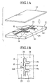
- Figs. 1A and 1B show a relationship between a vacuum forming die and a lower die film in a producing process according to the present invention, and Fig. 1A is a perspective view and Fig. 1B is a plan view.
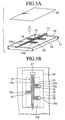
- Figs. 2A and 2B show a step of arranging electric wires of an embodiment, and Fig. 2A is a perspective view and Fig. 2B is a plan view.
- Figs. 3A and 3B show a step of disposing an upper die film of the embodiment, and Fig. 3A is a perspective view and Fig. 3B is a plan view.
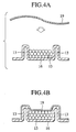
- Fig. 4A is a sectional view showing the lower die film and the upper die film before being bonded to each other, and Fig. 4B is a sectional view showing the lower and upper die films after being bonded to each other.
- Figs. 5A and 5B show a produced circuit body, and Fig. 5A is a perspective view and Fig. 5B is a plan view.
-
- Figs. 1A to 5B show, in the order of steps, an embodiment of a process for producing a circuit body in terms of a circuit structure according to the present invention. In the drawings, a
reference numeral 11 designates a vacuum forming die. - As shown in Figs. 1A and 1B, an upper face of the vacuum forming die 11 is a flat forming
face 12 which is provided with a plurality of projectingribs 13. The plurality ofribs 13 are fixed and projected on an upper face of the formingface 12 by bonding or threads. Anarranging recess portion 14 is formed between theopposed ribs 13. - The
arranging recess portion 14 formed by the plurality ofribs 13 is to provide a predetermined arranged shape in terms of a circuit pattern to electric wires 15 (see Figs. 2A and 2B). The shown arrangingrecess portion 14 comprises, a mainwiring forming portion 14a in a shape of a straight line and a plurality of branchwiring forming portions 14b perpendicular to the mainwiring forming portion 14a, as shown in Fig. 1B. - The projecting
ribs 13 are formed on the formingface 12 and a space between theribs 13 is utilized as the arrangingrecess portion 14, so that it is unnecessary to recess the formingface 12 to form the arrangingrecess portion 14. Therefore, it is advantageous that the arrangingrecess portion 14 can be formed easily, and the arrangingrecess portion 14 can be changed easily by exchanging or moving projecting positions of theribs 13. Also, upper andlower films face 12 with thefilms ribs 13, and it is possible to provide strength to the upper andlower films - A plurality of sucking
holes 25 are formed on the formingface 12 of thevacuum forming die 11. The suckingholes 25 are formed to be scattered outside and inside (the arranging recess portion 14) the opposedribs 13. The upper andlower films face 12 by a vacuum suction through the sucking holes 25. - Next, the producing process of the embodiment will be described.
- As shown in Fig. 1A, the forming
face 12 of thevacuum forming die 11 provided with the projectingribs 13 is covered with thelower die film 16. Thelower die film 16 is lightly sucked through the suckingholes 25, and is brought into close contact with the formingface 12. - Then, as shown in Figs. 2A and 2B, the plurality of
electric wires 15 are arranged on thevacuum forming die 11. This arrangement is carried out by disposing the plurality ofelectric wires 15 in the arrangingrecess portion 14. In the present embodiment,connectors electric wires 15 are used. In this case, theconnector 17 is previously connected to a terminal of amain wiring 15a of theelectric wire 15. Theconnector 18 is previously connected to each of terminal portions ofplural branch wirings 15b which branch off from themain wiring 15a. - The
electric wires 15 are arranged in the arrangingrecess portion 14 so that theconnectors 18 arranged on the terminal portions of thebranch wirings 15b are positioned in the arrangingrecess portion 14. More specifically, theconnectors 18 arranged on thebranch wirings 15b are disposed to be fitted between theribs 13, thewirings 15b are arranged therebetween. -
Connectors 18 are fitted between theribs 13 and are provisionally fixed to theribs 13, so that unexpected displacement of theconnectors 18 is limited. Consequently, theconnectors 18 do not deviate from proper positions due to the suction and vibration, and are provisionally fixed in the positions with accuracy. As a result, it is possible to fix theconnectors 18 to appropriate positions relative to awire harness 20 produced succeedingly. - The
connector 17 arranged on themain wiring 15a is not fitted between theribs 13 in the embodiment, but may be fitted between theribs 13 to be fixed provisionally, similarly to theconnectors 18 arranged on thebranch wirings 15b. - After the
electric wires 15 are arranged in the arrangingrecess portion 14 and are provisionally fixed to theconnectors 18 as described above, theupper die film 19 is put on theelectric wires 15 and the formingface 12 and peripheral portion of theupper film 19 is brought into contact with thelower die film 16, as shown in Figs. 3A and 3B. Then, theupper die film 19 is sucked through the suckingholes 25 and is brought into close contact with and bonded to theelectric wires 15 and thelower die film 16. - Figs. 4A and 4B show steps of bonding the
upper die film 19 to thelower die film 16. A hot-melt adhesive or other adhesives is applied on one or both of the opposed faces of theupper die film 19 and thelower die film 16. thevacuum forming die 11 is heated with thefilms lower films wires 15 is held by thefilms wire harness 20. Then, as described later, theconnectors 18 are fixed together with thewire harness 20,and aflat circuit body 23 is formed (see Figs. 5A and 5B). - In the embodiment, a width of the
upper die film 19 is set so that the upper film 9 can cover outer peripheral portions of theconnectors 18 arranged on thebranch wirings 15b, as shown in Fig. 3B. Specifically, the width is set so that theupper film 19 can cover the outer peripheral portions of theconnectors 18 except for theend portions 18a of theconnectors 18. Therefore, theend portions 18a of theconnectors 18 are not covered with theupper die film 19. Such anupper die film 19 is bonded to theconnectors 18 by the above-described vacuum suction and heating of thevacuum forming die 11. - As described above, the other portion of the
upper die film 19 is bonded to thelower die film 16. By bonding theupper die film 19 to theconnectors 18 in this manner, the upper andlower films connectors 18 interposed therebetween. - A
reference numeral 21 in Figs. 5A and 5B designates connector fixing portions of thefilm 19. Theconnector fixing portions 21 fix theconnectors 18 in proper positions to prevent theconnectors 18 from tottering. Therefore, theconnectors 18 can be easily fitted to the mating connectors without positioning. - The
connector fixing portions 21 are integrally provided to the outer peripheral portion of theupper die film 19, so that theconnector fixing portions 21 integral with the other portion of theupper die film 19 cover and reliably waterproof the terminal portions of theelectric wires 15. Therefore, a waterproof treatment for the terminal portions is unnecessary, and thewire harness 20 can be produced easily and speedily. - Further, since the
connector fixing portions 21 are not provided to theend portions 18a of theconnectors 18, theconnector fixing portions 21 do not closeconnection openings 22 on the side of theend portions 18a. Therefore, theconnector fixing portions 21 do not become hindrances to fitting of the mating connectors into theconnection openings 22. - After the arranged shape of the
wires 15 is held and theconnectors 18 are fixed by the above steps, the suction is stopped by thevacuum forming die 11, thewire harness 20 is released from thevacuum forming die 11, and the producing process is completed. - As described above, according to the present embodiment, the
connectors 18 do not totter because theconnectors 18 are fixed to the proper positions by theconnector fixing portions 21 provided to the upper and lower diefilms connectors 18 are integral with the upper andlower films connectors 18 can be reliably waterproofed. Consequently, the waterproof treatment for the terminal portions is unnecessary, and thewire harness 20 can be produced easily. - By forming the
connector fixing portions 21 on one of thefilms connector fixing portions 21 can be formed easily. - Furthermore, because the upper and
lower films electric wires 15, and simultaneously as which, the upper andlower films connectors 18 to fix theconnectors 18, a step for fixing theconnectors 18 is unnecessary, and theconnectors 18 can be fixed speedily and easily. - Since the
connectors 18 are provisionally fixed in the arrangingrecess portion 14, theconnectors 18 are not displaced when they are fixed by bonding the upper andlower films connectors 18 can be fixed accurately. - Also, because the space between the projecting ribs is used as the arranging
recess portion 14, the arrangingrecess portion 14 can be formed or changed easily.
Claims (5)
- A circuit body comprising:characterised in thata wire harness (20) having a plurality of electric wires (15) formed into an arranged shape, the electric wires (15) having a terminal portion;a connector (18) arranged on the terminal portion of the electric wires, the connector (18) having an outer peripheral portion and an end portion (18a); andan upper (19) and a lower (16) film (19, 16) bonded to each other with the electric wires (15) intervening therebetween to hold the electric wires (15) in the arranged shape,
at least one of the upper and lower films (19, 16) has a connector fixing portion (21) bonded to the outer peripheral portion of the connector (18) except for the end portion (18a) thereof to fix the connector (18). - A circuit body according to claim 1, wherein said connector fixing portion (21) is formed on both said upper and lower films (19, 16).
- A process for producing a circuit body comprising the steps of:arranging in an arranging recess portion (14) in a vacuum forming die (11) a plurality of electric wires (15) having a terminal portion arranged on a connector (18), with the electric wires (15) intervening between an upper film (19) and a lower film (16);interposing an outer peripheral portion of the connector (18) except for an end portion (18a) thereof between the upper film (19) and the lower film (16);vacuum sucking through the vacuum forming die (11) the upper film (19) and the lower film (16) to each other and to hold an arranged shape of the electric wires (15); andfixing the connector (18) between the upper film (19) and the lower film (16) by a connector fixing portion (21) bonded to the outer peripheral portion of the connector (18) except for the end portion (18a) thereof.
- A process for producing a circuit body according to claim 3, further comprising the step of disposing said connector (18) in the arranging recess portion (14) to provisionally fix the connector (18) when arranging the electric wires (15) in the vacuum forming die (11).
- A process for producing a circuit body according to claim 3 or 4, wherein said vacuum forming die (11) is provided with projecting ribs (13), the ribs (13) having a space therebetween used as the arranging recess portion (14).
Applications Claiming Priority (3)
| Application Number | Priority Date | Filing Date | Title |
|---|---|---|---|
| JP26713997 | 1997-09-30 | ||
| JP267139/97 | 1997-09-30 | ||
| JP9267139A JPH11111065A (en) | 1997-09-30 | 1997-09-30 | Circuit and manufacture therefor |
Publications (3)
| Publication Number | Publication Date |
|---|---|
| EP0904986A2 EP0904986A2 (en) | 1999-03-31 |
| EP0904986A3 EP0904986A3 (en) | 2001-11-21 |
| EP0904986B1 true EP0904986B1 (en) | 2004-11-24 |
Family
ID=17440629
Family Applications (1)
| Application Number | Title | Priority Date | Filing Date |
|---|---|---|---|
| EP98118470A Expired - Fee Related EP0904986B1 (en) | 1997-09-30 | 1998-09-30 | Circuit body and process for producing the circuit body |
Country Status (4)
| Country | Link |
|---|---|
| US (1) | US6272746B1 (en) |
| EP (1) | EP0904986B1 (en) |
| JP (1) | JPH11111065A (en) |
| DE (1) | DE69827736T2 (en) |
Families Citing this family (15)
| Publication number | Priority date | Publication date | Assignee | Title |
|---|---|---|---|---|
| FR2794085B1 (en) * | 1999-05-28 | 2001-08-17 | Valeo Climatisation | VEHICLE DASHBOARD WITH ELECTRICAL HARNESS |
| DE59907876D1 (en) * | 1999-12-01 | 2004-01-08 | Draexlmaier Lisa Gmbh | Method and tool for producing a mold carrier part with conductors and mold carrier part fixed thereon |
| DE10021064A1 (en) | 2000-04-28 | 2001-11-15 | Bosch Gmbh Robert | Cover device |
| JP3922565B2 (en) * | 2002-04-25 | 2007-05-30 | 矢崎総業株式会社 | Circuit molding method for resin molded panel and vacuum molding die |
| EP1568050B1 (en) * | 2002-12-02 | 2013-11-06 | Carl Freudenberg KG | Three-dimensional moulded planar cable, method for production and use thereof |
| US20050000632A1 (en) * | 2003-05-23 | 2005-01-06 | Tesa Ag | Method of bonding flat ribbon cables adhesively to substrates such as the interior decorative components of a passenger car, especially roof lining, door side part and boot lid |
| US6946604B1 (en) * | 2003-09-22 | 2005-09-20 | Maris George P | Template for preparing a wire harness |
| CN101616556B (en) * | 2008-06-27 | 2011-08-31 | 深圳富泰宏精密工业有限公司 | Housing of electronic device and manufacturing method thereof |
| EP2466702A1 (en) * | 2010-12-14 | 2012-06-20 | Tyco Electronics Nederland B.V. | Method and apparatus of manufacturing a cable assembly |
| JP5732901B2 (en) * | 2011-02-24 | 2015-06-10 | 株式会社オートネットワーク技術研究所 | Method for forming a short circuit in a wire harness |
| JP2012221916A (en) * | 2011-04-14 | 2012-11-12 | Auto Network Gijutsu Kenkyusho:Kk | Wire with protective member |
| JP2014050283A (en) * | 2012-09-03 | 2014-03-17 | Yazaki Corp | Harness protector |
| FR3003994B1 (en) * | 2013-03-26 | 2015-03-20 | Airbus Operations Sas | DEVICE FOR AIDING THE MANUFACTURE OF ELECTRIC HARNESSES |
| US20180093622A1 (en) * | 2016-09-30 | 2018-04-05 | Tony Matijevich | Wire harness with cylinder valve protection |
| US11742113B2 (en) * | 2019-10-28 | 2023-08-29 | The Boeing Company | Form board preparation for wire bundling |
Family Cites Families (9)
| Publication number | Priority date | Publication date | Assignee | Title |
|---|---|---|---|---|
| US3168617A (en) * | 1962-08-27 | 1965-02-02 | Tape Cable Electronics Inc | Electric cables and method of making the same |
| US4319075A (en) * | 1981-01-26 | 1982-03-09 | Amp Inc. | Sealed routing of undercarpet cable |
| JP2682555B2 (en) * | 1992-05-11 | 1997-11-26 | 矢崎総業株式会社 | Method for manufacturing flat circuit body |
| JP3144445B2 (en) * | 1993-01-29 | 2001-03-12 | 矢崎総業株式会社 | Flat wire harness manufacturing method and flat wire harness with fixture |
| GB2275373B (en) * | 1993-02-18 | 1996-11-27 | Sumitomo Wiring Systems | Flat harness assembly |
| JP2921551B2 (en) * | 1994-06-14 | 1999-07-19 | 池田物産株式会社 | Fusion method of floor carpet and mat |
| JP3565951B2 (en) * | 1995-07-20 | 2004-09-15 | 矢崎総業株式会社 | Wire harness and method of manufacturing the same |
| JP3249044B2 (en) * | 1996-06-04 | 2002-01-21 | 矢崎総業株式会社 | Wire harness and method for manufacturing the same |
| US5917151A (en) * | 1997-08-29 | 1999-06-29 | Ut Automotive Dearborn, Inc. | Multi-shot molds for manufacturing wire harnesses |
-
1997
- 1997-09-30 JP JP9267139A patent/JPH11111065A/en active Pending
-
1998
- 1998-09-29 US US09/161,723 patent/US6272746B1/en not_active Expired - Fee Related
- 1998-09-30 DE DE69827736T patent/DE69827736T2/en not_active Expired - Fee Related
- 1998-09-30 EP EP98118470A patent/EP0904986B1/en not_active Expired - Fee Related
Also Published As
| Publication number | Publication date |
|---|---|
| DE69827736T2 (en) | 2005-11-03 |
| EP0904986A2 (en) | 1999-03-31 |
| DE69827736D1 (en) | 2004-12-30 |
| US6272746B1 (en) | 2001-08-14 |
| EP0904986A3 (en) | 2001-11-21 |
| JPH11111065A (en) | 1999-04-23 |
Similar Documents
| Publication | Publication Date | Title |
|---|---|---|
| EP0904986B1 (en) | Circuit body and process for producing the circuit body | |
| EP1157892B1 (en) | Wire harness joint | |
| US5962813A (en) | Connection structure of flat cable to terminals | |
| US5645441A (en) | Rotary connector device | |
| JP2002170627A (en) | Waterproof connector and manufacturing method of the same | |
| EP1403967B1 (en) | Connecting structure for accessory device and cable waterproofing structure for accessory device and mounting structure for accessory device | |
| JP3698030B2 (en) | Junction box and junction box assembly method | |
| JP3109720B2 (en) | Electrical junction box | |
| CN112956040B (en) | Bus bar assembly and method of manufacturing the same | |
| KR20150023488A (en) | Motor vehicle component support and method for the production thereof | |
| JP4218852B2 (en) | Circuit unit | |
| JP3745446B2 (en) | Flat circuit body manufacturing method and vacuum forming die | |
| JP3416001B2 (en) | Method for manufacturing semiconductor device | |
| JPH09306261A (en) | Method for vacuum forming wire harness and wire harness formed thereby | |
| JPH11195327A (en) | Wire harness and its manufacture | |
| JPH10261327A (en) | Wire harness | |
| JPH11219739A (en) | Structure of bus bar electric connection part | |
| JP2751104B2 (en) | Method for manufacturing lead frame for semiconductor device | |
| JP3281832B2 (en) | Electrical fittings | |
| US5887342A (en) | Method for making an electronic control unit | |
| JP2001128343A (en) | Structure and method for wire harness attachment | |
| JP3003691B1 (en) | Connector cover | |
| JP2914190B2 (en) | Electrical junction box | |
| JPH03104296A (en) | Integrated circuit with metallic substrate | |
| JP2746965B2 (en) | Connector structure of integrated circuit having metal substrate |
Legal Events
| Date | Code | Title | Description |
|---|---|---|---|
| PUAI | Public reference made under article 153(3) epc to a published international application that has entered the european phase |
Free format text: ORIGINAL CODE: 0009012 |
|
| 17P | Request for examination filed |
Effective date: 19980930 |
|
| AK | Designated contracting states |
Kind code of ref document: A2 Designated state(s): AT BE CH CY DE DK ES FI FR GB GR IE IT LI LU MC NL PT SE Kind code of ref document: A2 Designated state(s): DE FR GB |
|
| AX | Request for extension of the european patent |
Free format text: AL;LT;LV;MK;RO;SI |
|
| PUAL | Search report despatched |
Free format text: ORIGINAL CODE: 0009013 |
|
| AK | Designated contracting states |
Kind code of ref document: A3 Designated state(s): AT BE CH CY DE DK ES FI FR GB GR IE IT LI LU MC NL PT SE |
|
| AX | Request for extension of the european patent |
Free format text: AL;LT;LV;MK;RO;SI |
|
| AKX | Designation fees paid |
Free format text: DE FR GB |
|
| 17Q | First examination report despatched |
Effective date: 20030904 |
|
| GRAP | Despatch of communication of intention to grant a patent |
Free format text: ORIGINAL CODE: EPIDOSNIGR1 |
|
| GRAS | Grant fee paid |
Free format text: ORIGINAL CODE: EPIDOSNIGR3 |
|
| GRAA | (expected) grant |
Free format text: ORIGINAL CODE: 0009210 |
|
| AK | Designated contracting states |
Kind code of ref document: B1 Designated state(s): DE FR GB |
|
| REG | Reference to a national code |
Ref country code: GB Ref legal event code: FG4D |
|
| REF | Corresponds to: |
Ref document number: 69827736 Country of ref document: DE Date of ref document: 20041230 Kind code of ref document: P |
|
| PG25 | Lapsed in a contracting state [announced via postgrant information from national office to epo] |
Ref country code: GB Free format text: LAPSE BECAUSE OF NON-PAYMENT OF DUE FEES Effective date: 20050930 |
|
| PLBE | No opposition filed within time limit |
Free format text: ORIGINAL CODE: 0009261 |
|
| STAA | Information on the status of an ep patent application or granted ep patent |
Free format text: STATUS: NO OPPOSITION FILED WITHIN TIME LIMIT |
|
| ET | Fr: translation filed | ||
| 26N | No opposition filed |
Effective date: 20050825 |
|
| PG25 | Lapsed in a contracting state [announced via postgrant information from national office to epo] |
Ref country code: DE Free format text: LAPSE BECAUSE OF NON-PAYMENT OF DUE FEES Effective date: 20060401 |
|
| GBPC | Gb: european patent ceased through non-payment of renewal fee |
Effective date: 20050930 |
|
| PG25 | Lapsed in a contracting state [announced via postgrant information from national office to epo] |
Ref country code: FR Free format text: LAPSE BECAUSE OF NON-PAYMENT OF DUE FEES Effective date: 20060531 |
|
| REG | Reference to a national code |
Ref country code: FR Ref legal event code: ST Effective date: 20060531 |