EP0903801A2 - Nonreciprocal circuit device - Google Patents
Nonreciprocal circuit device Download PDFInfo
- Publication number
- EP0903801A2 EP0903801A2 EP98117381A EP98117381A EP0903801A2 EP 0903801 A2 EP0903801 A2 EP 0903801A2 EP 98117381 A EP98117381 A EP 98117381A EP 98117381 A EP98117381 A EP 98117381A EP 0903801 A2 EP0903801 A2 EP 0903801A2
- Authority
- EP
- European Patent Office
- Prior art keywords
- ferrite
- electrodes
- capacitors
- single plate
- nonreciprocal circuit
- Prior art date
- Legal status (The legal status is an assumption and is not a legal conclusion. Google has not performed a legal analysis and makes no representation as to the accuracy of the status listed.)
- Granted
Links
Images


Classifications
-
- H—ELECTRICITY
- H01—ELECTRIC ELEMENTS
- H01P—WAVEGUIDES; RESONATORS, LINES, OR OTHER DEVICES OF THE WAVEGUIDE TYPE
- H01P1/00—Auxiliary devices
- H01P1/32—Non-reciprocal transmission devices
- H01P1/36—Isolators
-
- H—ELECTRICITY
- H01—ELECTRIC ELEMENTS
- H01P—WAVEGUIDES; RESONATORS, LINES, OR OTHER DEVICES OF THE WAVEGUIDE TYPE
- H01P1/00—Auxiliary devices
- H01P1/32—Non-reciprocal transmission devices
- H01P1/38—Circulators
- H01P1/383—Junction circulators, e.g. Y-circulators
- H01P1/387—Strip line circulators
Definitions
- the present invention relates to a nonreciprocal circuit device used at the microwave band such as, for instance, an isolator or a circulator.
- a lumped constant isolator used in mobile communication equipment such as mobile telephones, has a function which allows signals to pass only in the transmission direction while preventing transmission in the reverse direction. Furthermore, given the recent usage of mobile communication equipment, there are growing demands for smaller, lighter and less expensive devices. In the case of the isolator, there are similar demands for a smaller, lighter and cheaper device.
- this type of lumped constant isolator has a structure comprising top and bottom yokes 50 and 51 which contain, in sequence from the top, a permanent magnet 52, a central electrode body 53, a matching circuit board 54 and a ground board 55.
- the central electrode body 53 comprises three central electrodes 57.. which intersect in an electrically insulated state on a disc-shaped ferrite 56.
- the matching circuit board 54 comprises a rectangular thin-board dielectric substrate 54a, having a round hole 54b, which the central electrode body 53 is inserted into, formed in the center thereof; and capacitor electrodes 58.., which input/output ports P1 - P3 of the central electrodes 57 are connected to, formed around the round hole 54b in the dielectric substrate 54a. Further, an end resistance film 59 is connected to the port P3.
- a further problem is that the parts other than the capacitor electrodes 58 unnecessarily increase the area and weight of the conventional dielectric substrate 54a, making it more difficult to produce a smaller and light device.
- capacitor electrodes 58 are formed on a dielectric substrate 54a having high permittivity, adjacent capacitor electrodes 58 are prone to electrostatic coupling Cp, which is damaging to the attenuation properties of the isolator outside the band.
- This single plate capacitor can be manufactured by forming electrodes on the two main surfaces of a motherboard, which comprises a large flat board, and cutting the motherboard to predetermined dimensions. Such a single plate capacitor can therefore be mass-produced. Consequently, processing and handling are easier than when round holes and multiple capacitors are provided to a conventional dielectric substrate, and cost can be reduced. In addition, since electrodes are formed over the entire faces of the substrate, unnecessary increase of area and weight can be eliminated, thereby enabling the isolator to be made smaller and lighter by a proportionate amount. Moreover, since the capacitors are provided separately, it is possible to prevent electrostatic coupling between them and thereby avoid deterioration of attenuation properties outside the band.
- Fig. 4 and Fig. 5 show an example of an isolator using a single plate capacitor and are not the prior art. Like members corresponding to those in Fig. 6 are designated by like reference characters.
- This isolator comprises a resin terminal block 60, having a round hole 61 provided in the base wall 60a thereof, the central electrode body 53 being inserted into the round hole 61; rectangular single plate capacitors C1 - C3, provided on the periphery of the round hole 61 so as to surround the central electrode body 53; and a single plate resistor R.
- a substrate of approximate thickness 0.2 mm is generally used. Reducing the thickness even further would cause an extreme reduction in the strength of the substrate, worsening yield and consequently lowering productivity as well as lowering the reliability of product quality.
- laminated capacitors generally have Q of 20 - 100 at the microwave band. This is much lower than the single plate capacitor using dielectric material for high-frequency, which has Q of more than 200, causing further loss of characteristics of isolator. Furthermore, although the conventional laminated capacitor has relatively small top area S of approximately 0.5 mm 2 , it is approximately 0.5 mm tall, and hence has volume V of 0.25 mm 3 . By contrast, the single plate capacitor has S of 1.2 mm 2 and V of approximately 0.24 mm 3 . Therefore, the size reduction achieved when using a laminated capacitor is hardly significant.
- the present invention has been realized after consideration of the above points and aims to provide a nonreciprocal circuit device capable of reducing layout space when using single plate capacitors, and meeting demands for a smaller and lighter device.
- the nonreciprocal circuit device of the present invention comprises a plurality of central electrodes provided to a ferrite, which a permanent magnet applies a direct current magnetic field to, ports of the central electrodes being connected to capacitors for matching; wherein the capacitors for matching comprise single plate capacitors, formed by providing electrodes on both main surfaces of a dielectric substrate such that the electrodes completely cover the main surfaces and oppose each other with the dielectric substrate disposed therebetween; and electrode surfaces of the single plate capacitors are provided at an angle of 60 - 90 degrees to an mounting surface.
- a second aspect of the present invention comprises the nonreciprocal circuit device according to the first aspect, wherein at least a portion of electrodes at the cold ends of the single plate capacitors face the outside of the device.
- a third aspect of the present invention comprises the nonreciprocal circuit device according to the first aspect, wherein at least a portion of electrodes at the hot ends of the single plate capacitors face the outside of the device.
- a fourth aspect of the present invention comprises the nonreciprocal circuit device according to any one of the first to third aspects, wherein the ferrite is square when viewed from the top and the single plate capacitors are provided so as to enclose the sides of the ferrite.
- a fifth aspect of the present invention comprises the nonreciprocal circuit device according to any one of the first to fourth aspects, wherein the permanent magnet is square when viewed from the top.
- a sixth aspect of the nonreciprocal circuit element comprising a ferrite, a permanent magnet applying a direct current magnetic field to the ferrite, a plurality of central electrodes respectively having ports disposed on the ferrite and a matching capacitor with capacitor electrodes formed on both surfaces of a dielectric substrate such that the capacitor electrodes are opposed to each other and sandwich the dielectric substrate, wherein the ferrite has a square shape and the capacitor electrodes of the matching capacitors are inclined at an angle of 60 to 90 degrees toward a mounting surface and the matching capacitors are disposed so as to surround sides of the ferrite.
- a seventh aspect of the nonreciprocal circuit device of the present invention comprises a plurality of central electrodes provided to a ferrite, which a permanent magnet applies a direct current magnetic field to, ports of the central electrodes being connected to capacitors for matching; wherein the capacitors for matching are single plate capacitors, comprising electrodes provided on both main surfaces of a dielectric substrate such that electrodes completely cover the main surfaces and oppose each other with the dielectric substrate disposed therebetween; the ferrite is square when viewed from the top, and the single plate capacitors are provided so as to enclose the ferrite.
- a eighth aspect of the present invention comprises the nonreciprocal circuit device according to the seventh aspect, wherein the single plate capacitors are rectangular and extend along the sides of the ferrite.
- a ninth aspect of the present invention comprises the nonreciprocal circuit device according to either of the seventh and eighth aspects, wherein the permanent magnet is square.
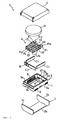
- Fig. 1, Fig. 2 and Fig. 4 are diagrams explaining a lumped constant isolator according to a first embodiment of the present invention, Fig. 1 showing an exploded perspective view of the isolator, and Fig. 2, a top view of the isolator when the top yoke is removed.
- the lumped constant isolator 1 of the present embodiment comprises a resin terminal substrate 3 provided on a magnetic metallic bottom yoke 2, having right-side and left-side walls 2a and 2a and a base wall 2b.
- a central electrode assemblage 4 is provided on the terminal substrate 3, and a box-shaped top yoke 5, comprising the same magnetic metal as the bottom yoke 2, is provided on top, thereby forming a magnetic closed circuit.
- a disc-shaped permanent magnet 6, which applies a direct current magnetic field to the central electrode assemblage 4, is affixed to the inner surface of the top yoke 5.
- the above isolator 1 is a parallelepiped with outer dimensions: top of less than 7.5 x 7.5 mm; height of less than 2.5 mm.
- the isolator 1 is surface-mounted on the line of a circuit board which is not shown in the diagram.
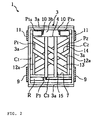
- the central electrode assemblage 4 comprises three central electrodes 13 - 15, which intersect alternately every 120 degrees, provided in an electrically insulated state on the upper surface of a microwave ferrite 12, which is square when viewed from above.
- Input/output ports P1 - P3 of one terminal side of each of the central electrodes 13 - 15 project outwards, and a shield 16, which is shared by the other terminal sides of the central electrodes 13 - 15, abuts to the lower surface of the ferrite 12.
- This shield 16 is connected to the base wall 2b of the bottom yoke 2.
- the central electrodes 13 - 15 are provided parallel toward the mounting surface.
- the input/output ports P1 - P3 of the central electrodes 13 - 15 are bent downwards at right angles to the mounting surface. Furthermore, tips P1a and P2a of two of the input/output ports P1 and P2 are parallel toward the mounting surface.
- the terminal substrate 3 comprises a base wall 3b, having a square hole 7 provided therein, secured in a single body to rectangular side walls 3a.
- the ferrite 12 is inserted into the square hole 7 and secured in position.
- the ground electrodes 8, provided on the inner surfaces of the left, right and lower side walls 3a are connected to the ground terminals 9 and 9 provided on the outer surfaces of the left and right side walls 3a.
- input/output ports 10 and 10 are provided at both ends of the upper edge of the base wall 3b. These ports 10 are connected to input/output terminals 11 and 11 which are provided on the outer surfaces of the left and right side walls 3a.
- the input/output terminals 11 and the ground terminals 9 are connected on the line of a circuit board which is not depicted in the diagram.
- Each of the single plate capacitors C1 - C3 is formed by providing capacitor electrodes on both main surfaces of a rectangular dielectric substrate in such a manner that the capacitor electrodes completely cover the main faces and oppose each other with the dielectric substrate disposed therebetween.
- the single plate capacitors C1 - C3 can be formed by patterning capacitor electrodes on a motherboard, comprising a large flat board, and cutting the motherboard into predetermined shapes.
- the single plate capacitors C1 - C3 are provided at an angle of 90 degrees, that is, perpendicular to the mounting surface. Furthermore, the electrodes at the cold ends of the single plate capacitors C1 - C3 are connected to the ground electrodes 8, and the electrodes at the hot ends are connected to the input/output ports P1 - P3. Consequently, the cold end electrode sides of the single plate capacitors C1 - C3 are facing the outside of the isolator since the ground electrode 8 is connected to the ground terminal 9.
- the cold end means a side of capacitor electrode connected to the ground electrode.
- the hot end means a side of capacitor electrode connected to the port.
- the tips P1a and P2a of the input/output ports P1 and P2 connect to the ports 10.
- the tip P3a of the remaining port P3 is connected to the end resistance R.
- the end resistance R is provided at an angle of 90 degrees to the mounting surface.
- the terminal substrate 3 comprises a base wall 3b, having a square hole 7 provided in the center thereof, secured in a single body to rectangular side walls 3a.
- Recesses 3c for positioning capacitors are provided in the left, right and lower edges of the square hole 7 in the base wall 3b, and a ground electrode 80 is provided on the bottom surface of each recess 3c. These ground electrodes 80 are connected to ground terminals 9 and 9 provided on the outer surfaces of the left and right side walls 3a.
- input/output ports 10 and 10 are provided at the left and right upper ends of the base wall 3b. These ports 10 are connected to input/output terminals 11 and 11 which are provided on the outer surfaces of the left and right side walls 3a.
- the input/output terminals 11 and the ground terminals 9 are surface-mounted on the line of a circuit board which is not depicted in the diagram.
- Single plate capacitors for matching C1 - C3 are accommodated in the positioning recesses 3c.
- the lower surface of the electrodes at the cold end sides of the single plate capacitors C1 - C3 are connected to the ground electrodes 80.
- an end resistance R is provided in parallel with the single plate capacitor C3 inside the positioning recess 3c. This end resistance R is connected to the ground terminal 9.
- the input/output ports Q1 - Q3 of the central electrodes 13 - 15 are connected to upper surface of the electrodes at the hot end sides of the single plate capacitors C1 - C3. Tips of two of the input/output ports Q1 and Q2 connect to the input/output ports 10, and the tip of the remaining Q3 is connected to the end resistance R.
- the ferrite 12 is square and is inserted in the square hole 7 provided in the terminal substrate 3. Consequently, the single plate capacitors C1 - C3 enclose the sides 12a of the ferrite 12 while also extending along these sides 12a.
- the nonreciprocal circuit device of the present invention includes that a ferrite has a circular shape and electrode surfaces of the single plate capacitors are disposed at an angle of 60 to 90 degrees to a mounting surface.
- shape of the ferrite is not limited to square, for example, circular shape as mentioned above or any other shapes may be employed.
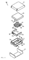
- Fig. 3 is a diagram illustrating a lumped constant isolator according to the third embodiment of the present invention.
- like members are designated by like reference characters.
- the configuration of the lumped constant isolator 20 of the present embodiment is basically the same as the first embodiment already described, comprising single plate capacitors C1 - C3 provided at an angle of 90 degrees to the mounting surface.
- a square permanent magnet 21 applies the direct current magnetic field to the ferrite 12.
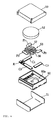
- Fig. 9 is a diagram illustrating a lumped constant isolator according to the fourth embodiment of the present invention.
- like members to those depicted in Fig. 1 are designated by like reference characters.
- the configuration of the lumped constant isolator 20 of the present embodiment is basically the same as the second embodiment already described, comprising single plate capacitors C1 ⁇ C3 extending along the sides of the ferrite 12, which is square.
- a permanent magnet 21, which applies direct current magnetic field to the ferrite 12, is square when viewed from the top.
- the ferrite 12 and the permanent magnet 21 are both square in shape. Consequently, an optimum magnetic field can be applied to the ferrite 12, improving electrical characteristics. Furthermore, since the permanent magnet 21 is square, it can easily be manufactured by calcinating a cluster of magnetic blocks and cutting out pieces of predetermined thickness, thereby lowering costs in the same way as above.
- the lumped constant isolator 1 of the present embodiment since the single plate capacitors C1 - C3 are provided at an angle of 90 degrees to the mounting surface, the area occupied by the single plate capacitors C1 - C3 when viewed from the top can be greatly reduced. Therefore, the isolator can be made smaller by a proportionate amount, meeting the demand mentioned above. By providing the single plate capacitors C1 - C3 in a perpendicular position, the top area of the terminal substrate 3 can be reduced and the weight can be reduced by a proportionate amount.
- the single plate capacitors C1 - C3 in a perpendicular position will increase the height of the isolator.
- the height of the single plate capacitors C1 - C3 can be accommodated enough by the thickness of the ferrite 12 and the gap between the ferrite 12 and the permanent magnet 6 without increasing the height of the isolator.
- the above gap is generally provided in order to prevent the permanent magnet from being so close to the high-frequency circuits that its electrical characteristics deteriorate. Therefore the thickness and the gap might be employed as play for accommodating the height of the single plate capacitors.
- the cold end electrodes of the single plate capacitors C1 - C3 face the outside of the isolator and the hot end electrodes face the inside, it is possible to prevent electromagnetic waves radiating from the hot ends from leaking to the outside. As a consequence, when the device is used in mobile communications equipment, unnecessary radiation inside the equipment can be reduced, contributing to stable operation.
- the single plate capacitors C1 - C3 are provided so as to enclose the sides 12a of the ferrite 12, which is square.
- the area around the ferrite 12 can be utilized more efficiently without changing the actual area and capacity of the ferrite 12, or the length and width of the central electrodes. Therefore, vacant space between the ferrite 12 and the single plate capacitors C1 - C3 can be eliminated, further contributing to making the isolator smaller and lighter.
- the ferrite 12 is square, it can easily be manufactured by calcinating a cluster of ferrite blocks and cutting out pieces of predetermined thickness, thereby lowering costs.
- the conventional disc-shaped ferrite there is a problem of high cost since ferrites must be formed individually from metal and then calcinated separately.
- the cold end electrodes of the single plate capacitors C1 - C3 faced the outside of the isolator.
- the hot end electrodes may face the outside. When the hot end electrodes face the outside, it is easier to send and receive signals to/from the outside.
- the above embodiment described an example in which the single plate capacitors C1 - C3 were provided perpendicular to the mounting surface, but alternatively they may be provided diagonal thereto. In such a case, the projected area when viewed from the top can be reduced, enabling the isolator to be made smaller.
- the single plate capacitors C1 - C3 are provided so as to enclose the sides 12a of the ferrite 12 which is square, the area around the ferrite 12 can be utilized more efficiently without changing the actual area and volume (capacity) of the ferrite, or the length and width of the central electrodes 13 - 15. In this case, there is almost no change in the electrical characteristics of the device as compared with a case where a conventional medium size ferrite is used. Consequently, vacant space between the ferrite 12 and the single plate capacitors C1 - C3 can be eliminated, whereby the total size can be reduced and made lighter by a proportionate amount, fulfilling the demand mentioned above.
- the single plate capacitors C1 ⁇ C3 are rectangular in shape and extend along the sides 12a of the ferrite 12, the area can be utilized more efficiently and size and weight can be further reduced.
- the present embodiment uses the single plate capacitors C1 - C3, manufacture is easy and mass-production is possible, as described above. Therefore, product cost can be reduced. Furthermore, processing and assembling are easier than when round holes and capacitor electrodes are formed on a thin flat board as in the conventional case. As a result, damage such as breakage can be avoided and reliability of product quality can be improved.
- the ferrite and the permanent magnet are both square, there is the advantage that an optimum magnetic field can be applied to the ferrite, improving the electrical properties.
Landscapes
- Non-Reversible Transmitting Devices (AREA)
Abstract
Description
Claims (9)
- A nonreciprocal circuit device, comprising a plurality of central electrodes (13-15) provided to a ferrite (12), which a permanent magnet (6;21) applies a direct current magnetic field to, ports (P1, P2, P3; Q1, Q2, Q3) of said central electrodes (13-15) being connected to capacitors for matching; wherein said capacitors for matching comprise single plate capacitors (C1, C2, C3), formed by providing electrodes on both main surfaces of a dielectric substrate such that said electrodes completely cover said main surfaces and oppose each other with said dielectric substrate disposed therebetween; and electrode faces of said single plate capacitors (C1, C2, C3) are provided at an angle of 60 - 90 degrees to a mounting surface.
- The nonreciprocal circuit device according to Claim 1, wherein at least a portion of electrodes at cold ends of said single plate capacitors (C1, C2, C3) face the outside of the device.
- The nonreciprocal circuit device according to Claim 1, wherein at least a portion of electrodes at hot ends of said single plate capacitors (C1, C2, C3) face the outside of the device.
- The nonreciprocal circuit device according to any one of Claims 1 - 3, wherein said ferrite (12) is square when viewed from the top and said single plate capacitors (C1, C2, C3) are provided so as to enclose the sides of said ferrite (12).
- The nonreciprocal circuit device according to any one of Claims 1 - 4, wherein said permanent magnet (6; 21) is square when viewed from the top.
- A nonreciprocal circuit element comprising,a ferrite (12);a permanent magnet (6; 21) applying a direct current magnetic field to said ferrite (12);a plurality of central electrodes (13-15) respectively having ports (P1, P2, P3; Q1, Q2, Q3) disposed on said ferrite (12); anda matching capacitor (C1, C2, C3) with capacitor electrodes formed on both surfaces of a dielectric substrate such that said capacitor electrodes are opposed to each other and sandwich said dielectric substrate,
wherein said ferrite (12) has a square shape and said capacitor electrodes of said matching capacitors (C1, C2, C3) are inclined at an angle of 60 to 90 degrees toward a mounting surface and said matching capacitors (C1, C2, C3) are disposed so as to surround sides of said ferrite (12). - A nonreciprocal circuit device, comprising a plurality of central electrodes (13-15) provided to a ferrite (12), which a permanent magnet (6; 21) applies a direct current magnetic field to, ports (P1, P2, P3; Q1, Q2, Q3) of the central electrodes being connected to capacitors for matching; wherein the capacitors for matching are single plate capacitors (C1, C2, C3), comprising electrodes provided on both main surfaces of a dielectric substrate such that said electrodes completely cover the main surfaces and oppose each other with the dielectric substrate disposed therebetween; the ferrite (12) is square when viewed from the top, and the single plate capacitors (13-15) are provided so as to enclose the ferrite (12).
- The nonreciprocal circuit device according to Claim 7, wherein the single plate capacitors (13-15) are rectangular and extend along the sides of the ferrite (12).
- The nonreciprocal circuit device according to Claims 7 and 8, wherein the permanent magnet (21) is square.
Applications Claiming Priority (6)
| Application Number | Priority Date | Filing Date | Title |
|---|---|---|---|
| JP25220597 | 1997-09-17 | ||
| JP252207/97 | 1997-09-17 | ||
| JP25220597A JP3164029B2 (en) | 1997-09-17 | 1997-09-17 | Non-reciprocal circuit device |
| JP25220797 | 1997-09-17 | ||
| JP25220797A JP3307293B2 (en) | 1997-09-17 | 1997-09-17 | Non-reciprocal circuit device |
| JP252205/97 | 1997-09-17 |
Publications (3)
| Publication Number | Publication Date |
|---|---|
| EP0903801A2 true EP0903801A2 (en) | 1999-03-24 |
| EP0903801A3 EP0903801A3 (en) | 2000-09-13 |
| EP0903801B1 EP0903801B1 (en) | 2004-02-04 |
Family
ID=26540598
Family Applications (1)
| Application Number | Title | Priority Date | Filing Date |
|---|---|---|---|
| EP98117381A Expired - Lifetime EP0903801B1 (en) | 1997-09-17 | 1998-09-14 | Nonreciprocal circuit device |
Country Status (5)
| Country | Link |
|---|---|
| US (1) | US6420941B2 (en) |
| EP (1) | EP0903801B1 (en) |
| KR (1) | KR100361432B1 (en) |
| CN (1) | CN1222075C (en) |
| DE (1) | DE69821423D1 (en) |
Cited By (10)
| Publication number | Priority date | Publication date | Assignee | Title |
|---|---|---|---|---|
| GB2350238A (en) * | 1999-02-15 | 2000-11-22 | Murata Manufacturing Co | Nonreciprocal circuit device |
| FR2802708A1 (en) * | 1999-12-16 | 2001-06-22 | Murata Manufacturing Co | Microwave/high frequency non reciprocal isolator/circulator construction having outer magnetic yokes with permanent magnet and capacitors magnetic element with central conductor held. |
| FR2805085A1 (en) * | 2000-01-19 | 2001-08-17 | Murata Manufacturing Co | NON-RECIPROCAL CIRCUIT DEVICE AND TELECOMMUNICATIONS DEVICE USING THE SAME |
| GB2361588A (en) * | 2000-03-03 | 2001-10-24 | Murata Manufacturing Co | Nonreciprocal circuit device and communication device |
| EP1047148A3 (en) * | 1999-04-23 | 2002-04-03 | Murata Manufacturing Co., Ltd. | Nonreciprocal circuit device and communication apparatus |
| US6597257B1 (en) * | 1999-09-21 | 2003-07-22 | Iurata Manufacturing Co., Ltd. | Nonreciprocal circuit device and communication apparatus incorporating same |
| US6670862B2 (en) * | 2000-03-22 | 2003-12-30 | Murata Manufacturing Co., Ltd. | Nonreciprocal circuit device and communication apparatus |
| EP1309032A3 (en) * | 2001-10-29 | 2004-01-02 | Alps Electric Co., Ltd. | Nonreciprocal circuit device |
| US6798311B2 (en) * | 1999-11-30 | 2004-09-28 | Murata Manufacturing Co., Ltd. | Nonreciprocal circuit device with a solenoid-shaped inductor generating perpendicular flux |
| US6819198B2 (en) * | 2000-02-25 | 2004-11-16 | Murata Manufacturing Co., Ltd. | Nonreciprocal circuit device and high-frequency circuit apparatus |
Families Citing this family (36)
| Publication number | Priority date | Publication date | Assignee | Title |
|---|---|---|---|---|
| ES2113023T3 (en) * | 1993-10-06 | 1998-04-16 | Dow Corning Toray Silicone | SILVER LOADED ORGANOSILOXANIC ORGANOSILOXANE COMPOSITIONS. |
| US7336468B2 (en) | 1997-04-08 | 2008-02-26 | X2Y Attenuators, Llc | Arrangement for energy conditioning |
| US6650525B2 (en) | 1997-04-08 | 2003-11-18 | X2Y Attenuators, Llc | Component carrier |
| US7301748B2 (en) | 1997-04-08 | 2007-11-27 | Anthony Anthony A | Universal energy conditioning interposer with circuit architecture |
| US9054094B2 (en) | 1997-04-08 | 2015-06-09 | X2Y Attenuators, Llc | Energy conditioning circuit arrangement for integrated circuit |
| US7336467B2 (en) | 2000-10-17 | 2008-02-26 | X2Y Attenuators, Llc | Energy pathway arrangement |
| US7042703B2 (en) | 2000-03-22 | 2006-05-09 | X2Y Attenuators, Llc | Energy conditioning structure |
| US20030161086A1 (en) | 2000-07-18 | 2003-08-28 | X2Y Attenuators, Llc | Paired multi-layered dielectric independent passive component architecture resulting in differential and common mode filtering with surge protection in one integrated package |
| US7321485B2 (en) | 1997-04-08 | 2008-01-22 | X2Y Attenuators, Llc | Arrangement for energy conditioning |
| US6603646B2 (en) | 1997-04-08 | 2003-08-05 | X2Y Attenuators, Llc | Multi-functional energy conditioner |
| US7110235B2 (en) | 1997-04-08 | 2006-09-19 | Xzy Altenuators, Llc | Arrangement for energy conditioning |
| US6894884B2 (en) | 1997-04-08 | 2005-05-17 | Xzy Attenuators, Llc | Offset pathway arrangements for energy conditioning |
| US7110227B2 (en) | 1997-04-08 | 2006-09-19 | X2Y Attenuators, Llc | Universial energy conditioning interposer with circuit architecture |
| US6954346B2 (en) | 1997-04-08 | 2005-10-11 | Xzy Attenuators, Llc | Filter assembly |
| US7274549B2 (en) | 2000-12-15 | 2007-09-25 | X2Y Attenuators, Llc | Energy pathway arrangements for energy conditioning |
| US7106570B2 (en) | 1997-04-08 | 2006-09-12 | Xzy Altenuators, Llc | Pathway arrangement |
| US6018448A (en) | 1997-04-08 | 2000-01-25 | X2Y Attenuators, L.L.C. | Paired multi-layered dielectric independent passive component architecture resulting in differential and common mode filtering with surge protection in one integrated package |
| US6606011B2 (en) | 1998-04-07 | 2003-08-12 | X2Y Attenuators, Llc | Energy conditioning circuit assembly |
| DE69937677T2 (en) | 1998-04-07 | 2008-11-20 | X2Y Attenuators, L.L.C. | COMPONENTS CARRIER |
| US7427816B2 (en) | 1998-04-07 | 2008-09-23 | X2Y Attenuators, Llc | Component carrier |
| KR100328257B1 (en) * | 1999-12-16 | 2002-03-16 | 이형도 | Isolator |
| US7113383B2 (en) | 2000-04-28 | 2006-09-26 | X2Y Attenuators, Llc | Predetermined symmetrically balanced amalgam with complementary paired portions comprising shielding electrodes and shielded electrodes and other predetermined element portions for symmetrically balanced and complementary energy portion conditioning |
| US7262949B2 (en) | 2000-08-15 | 2007-08-28 | X2Y Attenuators, Llc | Electrode arrangement for circuit energy conditioning |
| US7433168B2 (en) | 2000-10-17 | 2008-10-07 | X2Y Attenuators, Llc | Amalgam of shielding and shielded energy pathways and other elements for single or multiple circuitries with common reference node |
| US7193831B2 (en) | 2000-10-17 | 2007-03-20 | X2Y Attenuators, Llc | Energy pathway arrangement |
| JP2003087014A (en) * | 2001-06-27 | 2003-03-20 | Murata Mfg Co Ltd | Nonreciprocal circuit element and communication apparatus |
| JP2003204208A (en) * | 2002-01-07 | 2003-07-18 | Alps Electric Co Ltd | Non-reciprocal circuit element |
| US7180718B2 (en) | 2003-01-31 | 2007-02-20 | X2Y Attenuators, Llc | Shielded energy conditioner |
| JP2004289291A (en) | 2003-03-19 | 2004-10-14 | Alps Electric Co Ltd | Isolator and communication equipment |
| EP1629582A2 (en) | 2003-05-29 | 2006-03-01 | X2Y Attenuators, L.L.C. | Connector related structures including an energy conditioner |
| EP1698033A4 (en) | 2003-12-22 | 2010-07-21 | X2Y Attenuators Llc | ENERGY CONDITIONER WITH INTERNAL SHIELDING |
| US7630188B2 (en) | 2005-03-01 | 2009-12-08 | X2Y Attenuators, Llc | Conditioner with coplanar conductors |
| WO2006093831A2 (en) | 2005-03-01 | 2006-09-08 | X2Y Attenuators, Llc | Energy conditioner with tied through electrodes |
| US7586728B2 (en) | 2005-03-14 | 2009-09-08 | X2Y Attenuators, Llc | Conditioner with coplanar conductors |
| EP1991996A1 (en) | 2006-03-07 | 2008-11-19 | X2Y Attenuators, L.L.C. | Energy conditioner structures |
| CN116544030A (en) * | 2023-07-05 | 2023-08-04 | 西南应用磁学研究所(中国电子科技集团公司第九研究所) | Alternating Chip Capacitor Structure and Circulator/Isolator Composed of It |
Family Cites Families (8)
| Publication number | Priority date | Publication date | Assignee | Title |
|---|---|---|---|---|
| JP3175303B2 (en) * | 1992-05-12 | 2001-06-11 | 株式会社村田製作所 | Non-reciprocal circuit device |
| JPH06252610A (en) * | 1993-02-26 | 1994-09-09 | Tokin Corp | Non-reciprocal circuit element |
| US5450045A (en) | 1993-03-31 | 1995-09-12 | Tdk Corporation | Multi-layer microwave circulator |
| JP3064798B2 (en) | 1993-03-31 | 2000-07-12 | ティーディーケイ株式会社 | Circulator and manufacturing method thereof |
| EP0776060B1 (en) * | 1995-11-27 | 2002-06-05 | Murata Manufacturing Co., Ltd. | Non-reciprocal circuit element |
| JPH09213523A (en) * | 1996-02-01 | 1997-08-15 | Murata Mfg Co Ltd | Non-reciprocal circuit element |
| CA2214617C (en) * | 1996-09-06 | 2000-12-19 | Toshihiro Makino | Nonreciprocal circuit device |
| JPH10327003A (en) * | 1997-03-21 | 1998-12-08 | Murata Mfg Co Ltd | Irreversible circuit element and composite electronic component |
-
1998
- 1998-09-14 EP EP98117381A patent/EP0903801B1/en not_active Expired - Lifetime
- 1998-09-14 DE DE69821423T patent/DE69821423D1/en not_active Expired - Lifetime
- 1998-09-15 US US09/153,687 patent/US6420941B2/en not_active Expired - Lifetime
- 1998-09-17 CN CNB981195261A patent/CN1222075C/en not_active Expired - Lifetime
- 1998-09-17 KR KR10-1998-0038421A patent/KR100361432B1/en not_active Expired - Lifetime
Cited By (20)
| Publication number | Priority date | Publication date | Assignee | Title |
|---|---|---|---|---|
| US6583681B1 (en) | 1999-02-15 | 2003-06-24 | Murata Manufacturing Co., Ltd. | Nonreciprocal circuit device with vertical capacitors above half thickness of the ferrite |
| GB2350238B (en) * | 1999-02-15 | 2001-10-03 | Murata Manufacturing Co | Nonreciprocal circuit device |
| GB2350238A (en) * | 1999-02-15 | 2000-11-22 | Murata Manufacturing Co | Nonreciprocal circuit device |
| EP1047148A3 (en) * | 1999-04-23 | 2002-04-03 | Murata Manufacturing Co., Ltd. | Nonreciprocal circuit device and communication apparatus |
| US6633204B1 (en) | 1999-04-23 | 2003-10-14 | Murata Manufacturing Co., Ltd. | Nonreciprocal circuit device and communication apparatus |
| US6597257B1 (en) * | 1999-09-21 | 2003-07-22 | Iurata Manufacturing Co., Ltd. | Nonreciprocal circuit device and communication apparatus incorporating same |
| US6798311B2 (en) * | 1999-11-30 | 2004-09-28 | Murata Manufacturing Co., Ltd. | Nonreciprocal circuit device with a solenoid-shaped inductor generating perpendicular flux |
| FR2802708A1 (en) * | 1999-12-16 | 2001-06-22 | Murata Manufacturing Co | Microwave/high frequency non reciprocal isolator/circulator construction having outer magnetic yokes with permanent magnet and capacitors magnetic element with central conductor held. |
| GB2358738A (en) * | 1999-12-16 | 2001-08-01 | Murata Manufacturing Co | Nonreciprocal circuit device with conductive adhesive connections |
| GB2358738B (en) * | 1999-12-16 | 2002-05-29 | Murata Manufacturing Co | Nonreciprocal circuit device and communication apparatus incorporating the same |
| FR2805085A1 (en) * | 2000-01-19 | 2001-08-17 | Murata Manufacturing Co | NON-RECIPROCAL CIRCUIT DEVICE AND TELECOMMUNICATIONS DEVICE USING THE SAME |
| US6882262B2 (en) | 2000-01-19 | 2005-04-19 | Murata Manufacturing Co., Ltd. | Nonreciprocal circuit device and communication device using same |
| US6642831B2 (en) | 2000-01-19 | 2003-11-04 | Murata Manufacturing Co., Ltd. | Nonreciprocal circuit device and communication device using same |
| US6819198B2 (en) * | 2000-02-25 | 2004-11-16 | Murata Manufacturing Co., Ltd. | Nonreciprocal circuit device and high-frequency circuit apparatus |
| GB2361588A (en) * | 2000-03-03 | 2001-10-24 | Murata Manufacturing Co | Nonreciprocal circuit device and communication device |
| US6556098B2 (en) | 2000-03-03 | 2003-04-29 | Murata Manufacturing Co., Ltd. | Nonreciprocal circuit device with tapered side wall guide portions in the resin case |
| GB2361588B (en) * | 2000-03-03 | 2002-06-12 | Murata Manufacturing Co | Nonreciprocal circuit device and communication device |
| US6670862B2 (en) * | 2000-03-22 | 2003-12-30 | Murata Manufacturing Co., Ltd. | Nonreciprocal circuit device and communication apparatus |
| EP1309032A3 (en) * | 2001-10-29 | 2004-01-02 | Alps Electric Co., Ltd. | Nonreciprocal circuit device |
| US6876267B2 (en) | 2001-10-29 | 2005-04-05 | Alps Electric Co., Ltd. | Nonreciprocal circuit device |
Also Published As
| Publication number | Publication date |
|---|---|
| US20010054936A1 (en) | 2001-12-27 |
| KR19990029892A (en) | 1999-04-26 |
| KR100361432B1 (en) | 2003-03-17 |
| US6420941B2 (en) | 2002-07-16 |
| DE69821423D1 (en) | 2004-03-11 |
| EP0903801B1 (en) | 2004-02-04 |
| CN1222075C (en) | 2005-10-05 |
| CN1212479A (en) | 1999-03-31 |
| EP0903801A3 (en) | 2000-09-13 |
Similar Documents
| Publication | Publication Date | Title |
|---|---|---|
| EP0903801B1 (en) | Nonreciprocal circuit device | |
| EP0948079B1 (en) | Nonreciprocal circuit device | |
| US6657511B2 (en) | Nonreciprocal circuit device and communication apparatus including the same | |
| EP0776060B1 (en) | Non-reciprocal circuit element | |
| US7453326B2 (en) | Nonreciprocal circuit device | |
| JP3307293B2 (en) | Non-reciprocal circuit device | |
| EP0682380B1 (en) | Nonreciprocal circuit element | |
| JP3384367B2 (en) | Non-reciprocal circuit device and communication device | |
| US6642831B2 (en) | Nonreciprocal circuit device and communication device using same | |
| JP3419369B2 (en) | Non-reciprocal circuit device | |
| JP3275806B2 (en) | Non-reciprocal circuit device | |
| US6977559B2 (en) | Nonreciprocal circuit element with notch part in yoke | |
| KR100394803B1 (en) | Nonreciprocal circuit device and communication apparatus | |
| JP3164029B2 (en) | Non-reciprocal circuit device | |
| JPH11239009A (en) | Band widening structure of irreversible circuit element | |
| US6597253B2 (en) | Nonreciprocal circuit device and communication apparatus including the same | |
| JPH1197909A (en) | Non-reciprocal circuit element | |
| US20040066248A1 (en) | Miniature non-reciprocal circuit element with little variation in input impedance and communication apparatus | |
| JPH11298205A (en) | Irreversible circuit element | |
| JPH1079607A (en) | Non-reciprocal circuit element | |
| JPH1079606A (en) | Non-reciprocal circuit element | |
| JP2003234605A (en) | Non-reciprocal circuit element | |
| JP2002353706A (en) | Center electrode assembly, irreversible circuit element and communication unit |
Legal Events
| Date | Code | Title | Description |
|---|---|---|---|
| PUAI | Public reference made under article 153(3) epc to a published international application that has entered the european phase |
Free format text: ORIGINAL CODE: 0009012 |
|
| 17P | Request for examination filed |
Effective date: 19980914 |
|
| AK | Designated contracting states |
Kind code of ref document: A2 Designated state(s): DE FR GB |
|
| AX | Request for extension of the european patent |
Free format text: AL;LT;LV;MK;RO;SI |
|
| PUAL | Search report despatched |
Free format text: ORIGINAL CODE: 0009013 |
|
| AK | Designated contracting states |
Kind code of ref document: A3 Designated state(s): AT BE CH CY DE DK ES FI FR GB GR IE IT LI LU MC NL PT SE |
|
| AX | Request for extension of the european patent |
Free format text: AL;LT;LV;MK;RO;SI |
|
| AKX | Designation fees paid |
Free format text: DE FR GB |
|
| 17Q | First examination report despatched |
Effective date: 20020618 |
|
| GRAP | Despatch of communication of intention to grant a patent |
Free format text: ORIGINAL CODE: EPIDOSNIGR1 |
|
| GRAS | Grant fee paid |
Free format text: ORIGINAL CODE: EPIDOSNIGR3 |
|
| GRAA | (expected) grant |
Free format text: ORIGINAL CODE: 0009210 |
|
| AK | Designated contracting states |
Kind code of ref document: B1 Designated state(s): DE FR GB |
|
| PG25 | Lapsed in a contracting state [announced via postgrant information from national office to epo] |
Ref country code: FR Free format text: LAPSE BECAUSE OF FAILURE TO SUBMIT A TRANSLATION OF THE DESCRIPTION OR TO PAY THE FEE WITHIN THE PRESCRIBED TIME-LIMIT Effective date: 20040204 |
|
| REG | Reference to a national code |
Ref country code: GB Ref legal event code: FG4D |
|
| REF | Corresponds to: |
Ref document number: 69821423 Country of ref document: DE Date of ref document: 20040311 Kind code of ref document: P |
|
| PG25 | Lapsed in a contracting state [announced via postgrant information from national office to epo] |
Ref country code: DE Free format text: LAPSE BECAUSE OF FAILURE TO SUBMIT A TRANSLATION OF THE DESCRIPTION OR TO PAY THE FEE WITHIN THE PRESCRIBED TIME-LIMIT Effective date: 20040505 |
|
| PLBE | No opposition filed within time limit |
Free format text: ORIGINAL CODE: 0009261 |
|
| STAA | Information on the status of an ep patent application or granted ep patent |
Free format text: STATUS: NO OPPOSITION FILED WITHIN TIME LIMIT |
|
| 26N | No opposition filed |
Effective date: 20041105 |
|
| EN | Fr: translation not filed | ||
| PGFP | Annual fee paid to national office [announced via postgrant information from national office to epo] |
Ref country code: GB Payment date: 20170921 Year of fee payment: 20 |
|
| REG | Reference to a national code |
Ref country code: GB Ref legal event code: PE20 Expiry date: 20180913 |
|
| PG25 | Lapsed in a contracting state [announced via postgrant information from national office to epo] |
Ref country code: GB Free format text: LAPSE BECAUSE OF EXPIRATION OF PROTECTION Effective date: 20180913 |