EP0903748B1 - Nonvolatile semiconductor memory device - Google Patents
Nonvolatile semiconductor memory device Download PDFInfo
- Publication number
- EP0903748B1 EP0903748B1 EP98117243A EP98117243A EP0903748B1 EP 0903748 B1 EP0903748 B1 EP 0903748B1 EP 98117243 A EP98117243 A EP 98117243A EP 98117243 A EP98117243 A EP 98117243A EP 0903748 B1 EP0903748 B1 EP 0903748B1
- Authority
- EP
- European Patent Office
- Prior art keywords
- word lines
- memory cells
- memory
- data
- gate
- Prior art date
- Legal status (The legal status is an assumption and is not a legal conclusion. Google has not performed a legal analysis and makes no representation as to the accuracy of the status listed.)
- Expired - Lifetime
Links
- 239000004065 semiconductor Substances 0.000 title claims description 13
- 230000015654 memory Effects 0.000 claims description 109
- 239000011159 matrix material Substances 0.000 claims description 3
- 230000004044 response Effects 0.000 claims description 2
- 238000013500 data storage Methods 0.000 description 3
- 230000000694 effects Effects 0.000 description 3
- 230000005684 electric field Effects 0.000 description 2
- 239000000758 substrate Substances 0.000 description 2
- 238000009825 accumulation Methods 0.000 description 1
- 230000004075 alteration Effects 0.000 description 1
- 238000003491 array Methods 0.000 description 1
- 239000002800 charge carrier Substances 0.000 description 1
- 230000000295 complement effect Effects 0.000 description 1
- 230000008878 coupling Effects 0.000 description 1
- 238000010168 coupling process Methods 0.000 description 1
- 238000005859 coupling reaction Methods 0.000 description 1
- 230000007423 decrease Effects 0.000 description 1
- 230000000593 degrading effect Effects 0.000 description 1
- 238000010586 diagram Methods 0.000 description 1
- 230000007774 longterm Effects 0.000 description 1
- 238000000034 method Methods 0.000 description 1
- 229910021421 monocrystalline silicon Inorganic materials 0.000 description 1
- 238000000638 solvent extraction Methods 0.000 description 1
Images


Classifications
-
- G—PHYSICS
- G11—INFORMATION STORAGE
- G11C—STATIC STORES
- G11C16/00—Erasable programmable read-only memories
- G11C16/02—Erasable programmable read-only memories electrically programmable
- G11C16/06—Auxiliary circuits, e.g. for writing into memory
-
- G—PHYSICS
- G11—INFORMATION STORAGE
- G11C—STATIC STORES
- G11C16/00—Erasable programmable read-only memories
- G11C16/02—Erasable programmable read-only memories electrically programmable
- G11C16/06—Auxiliary circuits, e.g. for writing into memory
- G11C16/34—Determination of programming status, e.g. threshold voltage, overprogramming or underprogramming, retention
- G11C16/349—Arrangements for evaluating degradation, retention or wearout, e.g. by counting erase cycles
- G11C16/3495—Circuits or methods to detect or delay wearout of nonvolatile EPROM or EEPROM memory devices, e.g. by counting numbers of erase or reprogram cycles, by using multiple memory areas serially or cyclically
-
- G—PHYSICS
- G11—INFORMATION STORAGE
- G11C—STATIC STORES
- G11C16/00—Erasable programmable read-only memories
- G11C16/02—Erasable programmable read-only memories electrically programmable
- G11C16/06—Auxiliary circuits, e.g. for writing into memory
- G11C16/34—Determination of programming status, e.g. threshold voltage, overprogramming or underprogramming, retention
- G11C16/349—Arrangements for evaluating degradation, retention or wearout, e.g. by counting erase cycles
-
- G—PHYSICS
- G11—INFORMATION STORAGE
- G11C—STATIC STORES
- G11C2216/00—Indexing scheme relating to G11C16/00 and subgroups, for features not directly covered by these groups
- G11C2216/12—Reading and writing aspects of erasable programmable read-only memories
- G11C2216/28—Floating gate memory programmed by reverse programming, e.g. programmed with negative gate voltage and erased with positive gate voltage or programmed with high source or drain voltage and erased with high gate voltage
Definitions
- the present invention relates generally to nonvolatile semiconductor memory devices and, more particularly, to nonvolatile semiconductor memory devices capable of increasing the number of times memory cells can reliably be rewritten and limiting cell current reduction in an extended storage time period memory device.
- Nonvolatile semiconductor memory devices include ferro-electric random access memories (FRAM), erasable programmable read-only memories (EPROM), electrically erasable programmable read-only memories (EEPROM), and similar devices.
- FRAM ferro-electric random access memories
- EPROM erasable programmable read-only memories
- EEPROM electrically erasable programmable read-only memories
- EPROMs and EEPROMs store data by accumulating electrical charge carriers on the floating gate of a memory transistor.
- a control gate within the memory transistor is used to detect a variation in the threshold voltage of the memory due to the presence or absence of programming charge on the gate of the memory transistor.
- EEPROMs include "Flash” EEPROMs which provide an array of memory cells divided into sub-arrays or "blocks" where data erasure is performed in units of complete blocks.
- Flash-EEPROMs include memory cells which may be generally categorized into two types: the split gate type and the stacked gate type.
- a conventional Flash-EEPROM cell of the split gate type is illustrated in PCT Publication No. WO92/18980.
- FIG. 1 illustrates, in cross-section, a single memory cell 101 of the split gate type as shown in the Publication.
- the illustrated p-type single-crystal silicon substrate 102 has n-type source S and drain D regions formed on its surface.
- the source S and drain D define therebetween a channel region CH, above which a floating gate FG is formed.
- the floating gate FG is separated from the channel region CH by a first dielectric film 103.
- a control gate CG is formed extending partially over the floating gate FG with a second dielectric film 104 separating the control gate CG from the floating gate FG.
- a portion of the control gate CG is disposed over the channel CH and is separated from the channel CH by the first dielectric film 103 so that control gate CG can be used as a select gate 105 for the memory transistor.
- Data storage is accomplished by accumulating electrons in the floating gate FG using in part a voltage applied to the control gate CG and interacting with the floating gate FG through the second dielectric film 104.
- the cell current that flows through the memory cell decreases as the memory device is subjected to repeated data rewriting cycles.
- This reduced cell current may result in the memory cell being unable to reliably perform the data write and read operations required by normal operation of the memory cell.
- the reduced cell current is caused by repeated rewrite operations physically damaging or degrading the quality of the second dielectric film 104.
- a damaged dielectric film 104 may make it difficult for electrons to "escape" from the floating gate FG and may trap once-escaped electrons within the second dielectric film 104. The trapped electrons may then return to the floating gate FG, whereby the potential applied to the floating gate FG is effectively reduced so that the channel is not well formed beneath the floating gate FG.
- EP-A-0 463 580 describes an EEPROM memory device with a number of memory cells that are selected simultaneously for reading and writing to increase the reliability of the data storage. The simultaneous selection is achieved by connecting each memory cell to a common source line, a common data bit line and to a common word line.
- the memory device includes a high-reliability memory area, in which each 1 bit data memory unit is constituted by two memory cells, and an ordinary memory area in which each 1 bit data memory unit is a single memory cell.
- Two separate row decoders are provided for addressing the two memory areas. The row decoder that selects word lines in the high-reliability memory area is connected to two word lines simultaneously. The other row decoder is connected to individual word lines.
- the present invention provides a nonvolatile semiconductor memory device having: a memory cell array including a matrix of columns and rows of memory cells, wherein each row of memory cells is electrically connected to parallel common word lines and each column of memory cells is electrically connected to parallel common bit lines, the memory cell array further being divided into a special sector array for storing data of high reliability and comprising memory cells connected to a first set of word lines and a standard sector array comprising memory cells connected to a second set of word lines for storing data of normal reliability, a row decoder being provided for selecting word lines in response to the receipt of a row address, wherein the row decoder comprises a plurality of AND-gates the input of each AND gate being connected to a plurality of address nodes and the output of each AND-gate being connected to an individual word line, wherein pairs of AND gates connected to said first set of word lines have identical input connections and the AND gates connected to said second set of word lines have different input connections, such that the row decoder is arranged to select two word lines simultaneously when storing data in
- a nonvolatile memory device has one or more sectors reserved as a "special" sector (high reliability region).
- This high reliability sector is adapted so that when performing writing operations, data are written or "programmed" into two or more memory cells simultaneously; during reading, data are read out of all of the simultaneously written memory cells at the same time. Operation according to this aspect ensures that cell current is substantially doubled in magnitude thus enabling both an increase in the number of times that data can be rewritten and an increase in storage time as compared to that observed for conventional implementations of floating gate memories.
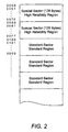
- FIG. 2 shows the configuration of a part of a nonvolatile semiconductor memory device embodying preferred aspects of the invention. More specifically, FIG. 2 shows an array of memory cells that is organized into both standard and special or high reliability sectors. Each of the sectors might store, for example, 128 bytes of data and has an address represented by a hexadecimal number. In the arrangement of FIG. 2, two sectors corresponding to addresses "0000" to "00FF" are reserved as special sectors. Those addresses following the address "0100" are used as ordinary sectors or standard regions in which one bit of data is stored into a single corresponding memory cell. Other embodiments of the invention might provide different numbers of special sectors or might provide different memory partitioning schemes.
- a memory cell array 302 includes a matrix of rows and columns of memory cells 101.
- the rows of memory cells 101 are electrically connected at their control gates CG to parallel common word lines WLa to WLz.
- the columns are coupled at drains D to parallel common bit lines BLa-BLz.
- All the memory cells 101 have sources S connected together to common source lines SL.
- Respective word lines WLa-WLz are connected to a row decoder 306 whereas bit lines BLa-BLz are connected to a column decoder 308.
- the memory cell array 302 is divided into a special sector array (for example, those cells associated with word lines WLa-WLn) and a standard sector array (e.g. word lines WLy-WLz).
- the row decoder 302 selects two of word lines WLa-WLn (e.g. WLm and WLn) that correspond to the row address as latched in latch 314, then connects the selected word lines WLm, WLn to a gate-voltage control circuit 316.
- the column decoder 308 is responsive to receipt of a column address as latched in address latch 314 and selects a corresponding one of the bit lines BLa-BLz (e.g.
- the gate voltage control circuit 316 is operable to control voltage potentials of the word lines WLm, WLn as connected via the row decoder 306 in a way that corresponds to a respective one of the operation modes shown in FIG. 4.
- the output potential of the drain voltage control circuit 318 controls the bit line BLm coupled via the column decoder 308 in a way corresponding to the operation modes illustrated in FIG. 4
- the common source line SL is connected to a source voltage control circuit 320. This circuit controls the potential applied to the common source line SL in a way corresponding to the operation modes shown in FIG. 4 to effect data writing operations.
- data are read out of any given one of the memory cells 101 and transferred from a corresponding one of the bit lines BLa-BLz through the column decoder 308 to a sense amplifier group 322.
- the sense amplifier group 322 includes a predefined number of sense amplifiers (not shown).
- the column decoder 308 provides an electrical connection between the presently selected bit line BLm and a corresponding sense amplifier.
- data judged (i.e., detected) by the sense amplifier group 322 is sent from an output buffer 324 via data pins 326 to external circuitry.
- two word lines e.g. WLm and WLn
- WLa-WLz select memory cells having sources coupled in common to each other.
- This selection permits the same data to be written into such two memory cells simultaneously in a relatively simple manner. Accordingly, reading the data from these two memory cells results in a readout cell current being doubled in magnitude.
- the read, write and other operations of the circuits illustrated in FIG. 3 (306 to 328) are under control of a core control circuit 330.
- the memory cells 332, 334 are related in the manner of memory cells within pages (sectors) having a common source and bit line.
- a scheme for selecting the word lines WLm, WLn associated with memory cells 332, 334 is to employ a row decoder 306 such as that shown in FIG. 5.
- FIG. 5 shows a row decoder 306 in accordance with the present teachings that allows pairs of memory cells to be selected through a hardware configuration modified from the conventional row address decoder configuration.
- four bit address data are provided through I/O pins and processed to provide signals to address nodes.
- the address nodes illustrated in FIG. 5 receive eight input address signals A0, *A0, ..., A3, *A3, where the mark "*" is used here to signify the binary complement of a signal and each of the address signals has either the "H” or the "L” level.
- the circuitry of FIG. 5 provides a number of sets of identical logic gates having identical connections.
- AND gates 1A and 1B are identical to each other in logical operation, due to the identical input signals provided to the gates.
- AND gates 2A, 2B provide the same logical operations.
- This hardware configuration makes it possible by using a single address to select both the word line WLm and word line WLn at the same time. Similar operations are performed for others of the groups, in this embodiment pairs, of "upper" AND gates 1A-8B shown in FIG. 5.
- addresses within the range of "0000" to "0111” correspond to special sectors and data stored in these sectors are high reliability data because the data signals are stored in two or more memory cells simultaneously. Addresses following the address "1000" correspond to standard sectors that are used in storing normal data. When addresses following "1000" are provided to the circuitry of FIG. 5, only one AND gate has its output go high for each distinct address. In this way, use of the row decoder configuration of FIG. 5 may permit users to selectively use any one of the special sectors for storing important data. Data can be stored in a high reliability manner by selecting the special sectors for the storage of the data.
- a selected word line WLm is supplied with a voltage of 14 to 15 volts, whereas the remaining (non-selected) word lines WLa-AL1, WLn-WLz are kept at ground potential.
- the potential on the control gate of a respective one of those memory cells 101 connected to the selected word line WLm is raised to 14 to 15 V.
- the electrostatic capacitance between the floating gate FG and portions of the memory cell including the source S and substrate 102 is almost always greater than the gate-to-gate electrostatic capacitance between the control gate CG and floating gate FG.
- the erase operation is done at the same time for all of the memory cells 101 coupled to the selected word line WLm. As necessary, the erase operation may be carried out for all of the memory cells 101 associated with multiple ones of the word lines WLa-WLz by simultaneous selection of these word lines.
- This erase scheme is called the "block" erase, reflecting the fact that the memory cell array 302 is divided into several blocks each coupled to and addressed by plural ones of the word lines WLa-WLz, permitting data erasure to be done in units of blocks.
- bit lines BLa-BLz are controlled so that bit lines associated with certain memory cells of interest-i.e., the memory cells to be programmed by injecting of electrons into their floating gates FG-are kept at ground potential whereas a high voltage is supplied to the remaining bit lines coupled to the other cells.
- individual data signals (such as bits) of important data are "duplicatively" stored in both the memory cell 332 and cell 334 at the same time. Such a duplicative storage strategy offers more stable data storage as well as allowing an increase in the rewrite number for the memory.
- the illustrative embodiment applies a voltage of 2 volts to the word lines WLm and WLn and sets the remaining non-selected word lines WLa-AL1, ALo-WLz at ground potential.
- the common source line SL is given a 12-V voltage. Writing may then be done with respect to the memory cells 332, 334 simultaneously.
- Each memory cell 101 includes a transistor having its source S and drain D, and control gate CG, where the transistor has a threshold voltage Vth that is typically about 0.5 volts.
- Vth threshold voltage
- electrons residing within the drain D move or "migrate" into the channel CH, which is in the inverted state. This inverted channel results in a current (cell current) flowing from source S to drain D.
- the potential underlying floating gate FG is raised due to the capacitive coupling between source S and floating gate FG. This creates a high electric field between control gate CG and floating gate FG.
- a voltage of 4 volts is applied to the word lines WLm, WLn and from the word lines to the control gates CG of the selected memory cells 101, while any remaining, non-selected word lines WLa-WL1, WLo-WLz are set at ground potential.
- a voltage of 2 V is applied to the one bit line BLm connected to the drains D of selected memory cells 332, 334, whereas the other non-selected bit lines BLa-BLl, BLn-BLz are coupled to ground.
- the floating gate FG of each of the erased ones of the memory cells 101 is charged to a positive polarity as the result of removing electrons from the floating gate FG.
- the floating gate FG of each one of the programmed memory cells 101 is, on the other hand, charged to a negative polarity by injecting electrons into the floating gate. Accordingly, in the individual erased memory cell 101, the channel CH immediately underlying the floating gate FG is rendered conductive (turned on) while the channel CH of each programmed cell is rendered nonconductive (turned off).
- memory cells 332, 334 are programmed so that the floating gate has a negative polarity.
- This programmed state is identified in the read operation by a relatively low level of current flow. More specifically, when the read voltage is applied to the gates of memory cells 332, 334, a cell current flows in the memory cells 332, 334 that is sufficiently small so that the cells are recognized as being programmed by the normal read circuits of the memory. On the other hand, assuming that these cells 332, 334 are not subject to programming (i.e., the cells are kept in the erased state) and their floating gates FG are charged to the positive polarity, an increased amount of current flows through the memory cells. This "erased" read current may be two times greater than the read current detected for a standard cell.
- the resulting read data is forwarded to a corresponding sense amplifier of the sense amplifier group 322, which attempts to identify the logic value of the data, "1" or "0", by determining whether the value of a cell current Id detected from a cell 101 is greater or less than a reference value.
- the judgment output from the comparison to the reference current effects the reading of cell data from each of the memory cells 101.
- the data readout is typically done using the definition that data from erased memory cells has the logical value of "1" whereas data from programmed cells is "0".
- the individual memory cells 101 are capable of storing therein binary data of either the logic value "1" as designated by the erase state or "0" as designated by the programmed state.
- FIG. 6 shows a relation of a rewrite number versus a cell current.
- the rewrite number represents how many times the date rewrite or re-programming is carried out and is plotted logarithmically along the horizontal axis of the graph of FIG. 6.
- a curve “A” indicates a cell current resulting from standard “one-at-a-time” read operations wherein a single memory cell is selected for read at a time.
- Curve “B” demonstrates a cell current resulting from a "two-at-a-time” read procedure in accordance with certain preferred embodiments of the invention, wherein two memory cells are read simultaneously.
- FIG. 6 represents the value of a reference current used in determining whether a stored data bit is a logic "0" or "1". Comparing the cell-current curves A and B with the reference value Iref, FIG. 6 shows that a Flash EEPROM according to an embodiment of the invention, identified by curve B in FIG. 6, can be rewritten approximately ten times more than the standard EEPROM identified by curve A. The curves of FIG. 6 demonstrate that the floating gate memory cell rewrite number may be significantly increased through practice of preferred embodiments of the invention.
- the invention is also capable of increasing the amount of time that data are stored through the accumulation and long-term storage of electrons on the floating gate of each memory cell.
- the write operation places the floating gate of the written memory cell in the "deep" positive polarity state due to removal of electrons therefrom. If the floating gate is in such a highly positive state, the gate may accommodate an increased number of electrons leaking from nearby structures onto the gate without threatening the integrity of the data stored in the memory cell.
- the gradual reduction in programming charge can continue for a longer period of time without affecting operation of the memory cell due to the positive state achieved in accordance with preferred embodiments of the invention.
- the potential drop associated with charge leaking onto the floating gate could otherwise make forming the underlying channel region more difficult, which reduces the current that flows in the memory cell.
- the cell current reduction is suppressed by one half, thus increasing the time period over which data can reliably stored.
- a nonvolatile semiconductor memory device which does not exhibit as significant of reduction in cell current even after many rewrite cycles.
- two or more memory cells may be designed so that the same data are written into and read from the same two or more memory cells, it becomes possible to increase the rewrite number while enabling important data to be stored therein for an extended time period.
Landscapes
- Read Only Memory (AREA)
- Non-Volatile Memory (AREA)
- For Increasing The Reliability Of Semiconductor Memories (AREA)
Description
- The present invention relates generally to nonvolatile semiconductor memory devices and, more particularly, to nonvolatile semiconductor memory devices capable of increasing the number of times memory cells can reliably be rewritten and limiting cell current reduction in an extended storage time period memory device.
- In recent years nonvolatile semiconductor memory devices have become more important. Nonvolatile memories include ferro-electric random access memories (FRAM), erasable programmable read-only memories (EPROM), electrically erasable programmable read-only memories (EEPROM), and similar devices. EPROMs and EEPROMs store data by accumulating electrical charge carriers on the floating gate of a memory transistor. A control gate within the memory transistor is used to detect a variation in the threshold voltage of the memory due to the presence or absence of programming charge on the gate of the memory transistor. EEPROMs include "Flash" EEPROMs which provide an array of memory cells divided into sub-arrays or "blocks" where data erasure is performed in units of complete blocks.
- Flash-EEPROMs include memory cells which may be generally categorized into two types: the split gate type and the stacked gate type. A conventional Flash-EEPROM cell of the split gate type is illustrated in PCT Publication No. WO92/18980. FIG. 1 illustrates, in cross-section, a
single memory cell 101 of the split gate type as shown in the Publication. Referring now to FIG. 1, the illustrated p-type single-crystal silicon substrate 102 has n-type source S and drain D regions formed on its surface. The source S and drain D define therebetween a channel region CH, above which a floating gate FG is formed. The floating gate FG is separated from the channel region CH by a firstdielectric film 103. A control gate CG is formed extending partially over the floating gate FG with a seconddielectric film 104 separating the control gate CG from the floating gate FG. A portion of the control gate CG is disposed over the channel CH and is separated from the channel CH by the firstdielectric film 103 so that control gate CG can be used as aselect gate 105 for the memory transistor. Data storage is accomplished by accumulating electrons in the floating gate FG using in part a voltage applied to the control gate CG and interacting with the floating gate FG through the seconddielectric film 104. - In those memory devices of the type shown in FIG. 1, which may store electrons in the floating gate FG, the cell current that flows through the memory cell decreases as the memory device is subjected to repeated data rewriting cycles. This reduced cell current may result in the memory cell being unable to reliably perform the data write and read operations required by normal operation of the memory cell. Presumably, the reduced cell current is caused by repeated rewrite operations physically damaging or degrading the quality of the second
dielectric film 104. In turn, a damageddielectric film 104 may make it difficult for electrons to "escape" from the floating gate FG and may trap once-escaped electrons within the seconddielectric film 104. The trapped electrons may then return to the floating gate FG, whereby the potential applied to the floating gate FG is effectively reduced so that the channel is not well formed beneath the floating gate FG. - Another disadvantage observed when using conventional floating gate memories is that the time period over which data can be reliably stored is limited. In other words, with conventional floating gate memories there is a risk of data alteration after the elapse of a certain time period resulting in lack of reliability. Data can be altered as electrons leak through the dielectric film to a floating gate FG that is in the erase state, which results in this gate unintentionally changing to an electron injected state.
- EP-A-0 463 580 describes an EEPROM memory device with a number of memory cells that are selected simultaneously for reading and writing to increase the reliability of the data storage. The simultaneous selection is achieved by connecting each memory cell to a common source line, a common data bit line and to a common word line. In one embodiment, the memory device includes a high-reliability memory area, in which each 1 bit data memory unit is constituted by two memory cells, and an ordinary memory area in which each 1 bit data memory unit is a single memory cell. Two separate row decoders are provided for addressing the two memory areas. The row decoder that selects word lines in the high-reliability memory area is connected to two word lines simultaneously. The other row decoder is connected to individual word lines.
- The present invention provides a nonvolatile semiconductor memory device having: a memory cell array including a matrix of columns and rows of memory cells, wherein each row of memory cells is electrically connected to parallel common word lines and each column of memory cells is electrically connected to parallel common bit lines, the memory cell array further being divided into a special sector array for storing data of high reliability and comprising memory cells connected to a first set of word lines and a standard sector array comprising memory cells connected to a second set of word lines for storing data of normal reliability,
a row decoder being provided for selecting word lines in response to the receipt of a row address, wherein the row decoder comprises a plurality of AND-gates the input of each AND gate being connected to a plurality of address nodes and the output of each AND-gate being connected to an individual word line, wherein pairs of AND gates connected to said first set of word lines have identical input connections and the AND gates connected to said second set of word lines have different input connections, such that the row decoder is arranged to select two word lines simultaneously when storing data in said high reliability section array and to select individual word lines when storing data of normal reliability in said standard sector. -
- FIG. 1 provides a sectional view of one memory cell of a nonvolatile semiconductor memory device.
- FIG. 2 shows an address map of a memory having two special sectors.
- FIG. 3 is a block diagram showing an overall configuration of a nonvolatile semiconductor memory device embodying aspects of the invention.
- FIG. 4 shows selected characteristics of some operational modes of memory cells of a nonvolatile semiconductor memory device embodying aspects of the invention.
- FIG. 5 shows a
row decoder 306 that might be used in a nonvolatile memory in accordance with a preferred embodiment of the present invention. - FIG. 6 is a graph showing a relation of a rewrite number versus cell current of the nonvolatile semiconductor memory device.
- An explanation of the present invention will be given in terms of various embodiments of a nonvolatile semiconductor memory device implementing one or more aspects of the invention. According to particularly preferred embodiments of the invention, a nonvolatile memory device has one or more sectors reserved as a "special" sector (high reliability region). This high reliability sector is adapted so that when performing writing operations, data are written or "programmed" into two or more memory cells simultaneously; during reading, data are read out of all of the simultaneously written memory cells at the same time. Operation according to this aspect ensures that cell current is substantially doubled in magnitude thus enabling both an increase in the number of times that data can be rewritten and an increase in storage time as compared to that observed for conventional implementations of floating gate memories.
- FIG. 2 shows the configuration of a part of a nonvolatile semiconductor memory device embodying preferred aspects of the invention. More specifically, FIG. 2 shows an array of memory cells that is organized into both standard and special or high reliability sectors. Each of the sectors might store, for example, 128 bytes of data and has an address represented by a hexadecimal number. In the arrangement of FIG. 2, two sectors corresponding to addresses "0000" to "00FF" are reserved as special sectors. Those addresses following the address "0100" are used as ordinary sectors or standard regions in which one bit of data is stored into a single corresponding memory cell. Other embodiments of the invention might provide different numbers of special sectors or might provide different memory partitioning schemes.
- Turning to FIG. 3, an overall configuration of a Flash
EEPROM 300 embodying aspects of the invention is shown which employs memory cells of the split gate type. A memory cell array 302 includes a matrix of rows and columns ofmemory cells 101. The rows ofmemory cells 101 are electrically connected at their control gates CG to parallel common word lines WLa to WLz. The columns are coupled at drains D to parallel common bit lines BLa-BLz. All thememory cells 101 have sources S connected together to common source lines SL. Respective word lines WLa-WLz are connected to arow decoder 306 whereas bit lines BLa-BLz are connected to acolumn decoder 308. Externally supplied row address and column address bits are input to the nonvolatile memory ataddress pins 310, and then the address bits are transferred frompins 310 through anaddress buffer 312 to anaddress latch circuit 314. Of those address bits latched atlatch 314, row address bits are sent to therow decoder 306, while column address bits are passed to thecolumn decoder 308. - The memory cell array 302 is divided into a special sector array (for example, those cells associated with word lines WLa-WLn) and a standard sector array (e.g. word lines WLy-WLz). Upon receipt of an address designating a special sector, the row decoder 302 selects two of word lines WLa-WLn (e.g. WLm and WLn) that correspond to the row address as latched in
latch 314, then connects the selected word lines WLm, WLn to a gate-voltage control circuit 316. Thecolumn decoder 308 is responsive to receipt of a column address as latched inaddress latch 314 and selects a corresponding one of the bit lines BLa-BLz (e.g. BLm), which bit line is then coupled to a drain-voltage control circuit 318. The gatevoltage control circuit 316 is operable to control voltage potentials of the word lines WLm, WLn as connected via therow decoder 306 in a way that corresponds to a respective one of the operation modes shown in FIG. 4. The output potential of the drainvoltage control circuit 318 controls the bit line BLm coupled via thecolumn decoder 308 in a way corresponding to the operation modes illustrated in FIG. 4 The common source line SL is connected to a sourcevoltage control circuit 320. This circuit controls the potential applied to the common source line SL in a way corresponding to the operation modes shown in FIG. 4 to effect data writing operations. - In data reading operations, data are read out of any given one of the
memory cells 101 and transferred from a corresponding one of the bit lines BLa-BLz through thecolumn decoder 308 to asense amplifier group 322. Thesense amplifier group 322 includes a predefined number of sense amplifiers (not shown). Thecolumn decoder 308 provides an electrical connection between the presently selected bit line BLm and a corresponding sense amplifier. As will be described later, data judged (i.e., detected) by thesense amplifier group 322 is sent from anoutput buffer 324 via data pins 326 to external circuitry. - In this illustrated embodiment of the invention, two word lines (e.g. WLm and WLn) are simultaneously selected from among those sets of word lines WLa-WLz that select memory cells having sources coupled in common to each other. This selection permits the same data to be written into such two memory cells simultaneously in a relatively simple manner. Accordingly, reading the data from these two memory cells results in a readout cell current being doubled in magnitude. The read, write and other operations of the circuits illustrated in FIG. 3 (306 to 328) are under control of a
core control circuit 330. - Consider now a
memory cell 332 andmemory cell 334 selected as the special-sector memory cells into which the same data signal is to be written in the embodiment illustrated in FIG. 3. Thememory cells memory cells row decoder 306 such as that shown in FIG. 5. - FIG. 5 shows a
row decoder 306 in accordance with the present teachings that allows pairs of memory cells to be selected through a hardware configuration modified from the conventional row address decoder configuration. As shown in the exemplary embodiment of FIG. 5, four bit address data are provided through I/O pins and processed to provide signals to address nodes. The address nodes illustrated in FIG. 5 receive eight input address signals A0, *A0, ..., A3, *A3, where the mark "*" is used here to signify the binary complement of a signal and each of the address signals has either the "H" or the "L" level. The circuitry of FIG. 5 provides a number of sets of identical logic gates having identical connections. That is, ANDgates gates - This hardware configuration makes it possible by using a single address to select both the word line WLm and word line WLn at the same time. Similar operations are performed for others of the groups, in this embodiment pairs, of "upper" AND
gates 1A-8B shown in FIG. 5. According to this implementation of aspects of the invention, addresses within the range of "0000" to "0111" correspond to special sectors and data stored in these sectors are high reliability data because the data signals are stored in two or more memory cells simultaneously. Addresses following the address "1000" correspond to standard sectors that are used in storing normal data. When addresses following "1000" are provided to the circuitry of FIG. 5, only one AND gate has its output go high for each distinct address. In this way, use of the row decoder configuration of FIG. 5 may permit users to selectively use any one of the special sectors for storing important data. Data can be stored in a high reliability manner by selecting the special sectors for the storage of the data. - An explanation is now given of respective operation modes (erase, write, and read modes) of the
Flash EEPROM 300 in conjunction with FIGS. 1 through 5. - When the EEPROM is set in the erase mode, the potentials of all the bit lines BLa-BLz and common source line SL are held at ground level (= 0 V). A selected word line WLm is supplied with a voltage of 14 to 15 volts, whereas the remaining (non-selected) word lines WLa-AL1, WLn-WLz are kept at ground potential. With the application of these voltages, the potential on the control gate of a respective one of those
memory cells 101 connected to the selected word line WLm is raised to 14 to 15 V. The electrostatic capacitance between the floating gate FG and portions of the memory cell including the source S andsubstrate 102 is almost always greater than the gate-to-gate electrostatic capacitance between the control gate CG and floating gate FG. Due to this, a high electric field is created between the control gate CG and floating gate FG when the control gate CG is at 14-15 V and the source is at 0 V. This results in a Fowler-Nordheim (FN) tunnel current flowing as electrons on the floating gate FG move toward control gate CG, erasing the data signal stored inmemory cell 101. - The erase operation is done at the same time for all of the
memory cells 101 coupled to the selected word line WLm. As necessary, the erase operation may be carried out for all of thememory cells 101 associated with multiple ones of the word lines WLa-WLz by simultaneous selection of these word lines. This erase scheme is called the "block" erase, reflecting the fact that the memory cell array 302 is divided into several blocks each coupled to and addressed by plural ones of the word lines WLa-WLz, permitting data erasure to be done in units of blocks. - In the data write mode the bit lines BLa-BLz are controlled so that bit lines associated with certain memory cells of interest-i.e., the memory cells to be programmed by injecting of electrons into their floating gates FG-are kept at ground potential whereas a high voltage is supplied to the remaining bit lines coupled to the other cells. Note that in preferred embodiments of the instant invention, individual data signals (such as bits) of important data are "duplicatively" stored in both the
memory cell 332 andcell 334 at the same time. Such a duplicative storage strategy offers more stable data storage as well as allowing an increase in the rewrite number for the memory. To effect duplicative storage, the illustrative embodiment applies a voltage of 2 volts to the word lines WLm and WLn and sets the remaining non-selected word lines WLa-AL1, ALo-WLz at ground potential. The common source line SL is given a 12-V voltage. Writing may then be done with respect to thememory cells - Each
memory cell 101 includes a transistor having its source S and drain D, and control gate CG, where the transistor has a threshold voltage Vth that is typically about 0.5 volts. Within individual ones of selectedmemory cells 101, electrons residing within the drain D move or "migrate" into the channel CH, which is in the inverted state. This inverted channel results in a current (cell current) flowing from source S to drain D. On the other hand, upon application of a 12 V voltage to source S, the potential underlying floating gate FG is raised due to the capacitive coupling between source S and floating gate FG. This creates a high electric field between control gate CG and floating gate FG. Thus, electrons within channel CH are electrically accelerated producing the so-called "hot" electrons, which are then injected into the floating gate FG as shown by arrow A in FIG. 1. As a result, a desired amount of charge is accumulated on floating gate FG of each selectedmemory cell 101 so that 1-bit data are written and stored in the cells. - When the Flash EEPROM is in the read mode, a voltage of 4 volts is applied to the word lines WLm, WLn and from the word lines to the control gates CG of the selected
memory cells 101, while any remaining, non-selected word lines WLa-WL1, WLo-WLz are set at ground potential. A voltage of 2 V is applied to the one bit line BLm connected to the drains D of selectedmemory cells - As discussed previously, the floating gate FG of each of the erased ones of the
memory cells 101 is charged to a positive polarity as the result of removing electrons from the floating gate FG. The floating gate FG of each one of the programmedmemory cells 101 is, on the other hand, charged to a negative polarity by injecting electrons into the floating gate. Accordingly, in the individual erasedmemory cell 101, the channel CH immediately underlying the floating gate FG is rendered conductive (turned on) while the channel CH of each programmed cell is rendered nonconductive (turned off). Consequently, application of a read voltage of 4 volts to the control gate CG causes a cell current to flow from drain D to source S in the erased cell that is greater in magnitude than the current that flows in a programmed memory cell upon application of a similar read voltage. - Referring once again to FIG. 3, then,
memory cells memory cells memory cells cells - The resulting read data is forwarded to a corresponding sense amplifier of the
sense amplifier group 322, which attempts to identify the logic value of the data, "1" or "0", by determining whether the value of a cell current Id detected from acell 101 is greater or less than a reference value. The judgment output from the comparison to the reference current effects the reading of cell data from each of thememory cells 101. Those skilled in the art will appreciate that the data readout is typically done using the definition that data from erased memory cells has the logical value of "1" whereas data from programmed cells is "0". In the illustrated embodiment of the invention, theindividual memory cells 101 are capable of storing therein binary data of either the logic value "1" as designated by the erase state or "0" as designated by the programmed state. - FIG. 6 shows a relation of a rewrite number versus a cell current. The rewrite number represents how many times the date rewrite or re-programming is carried out and is plotted logarithmically along the horizontal axis of the graph of FIG. 6. A curve "A" indicates a cell current resulting from standard "one-at-a-time" read operations wherein a single memory cell is selected for read at a time. Curve "B" demonstrates a cell current resulting from a "two-at-a-time" read procedure in accordance with certain preferred embodiments of the invention, wherein two memory cells are read simultaneously. "Iref" in FIG. 6 represents the value of a reference current used in determining whether a stored data bit is a logic "0" or "1". Comparing the cell-current curves A and B with the reference value Iref, FIG. 6 shows that a Flash EEPROM according to an embodiment of the invention, identified by curve B in FIG. 6, can be rewritten approximately ten times more than the standard EEPROM identified by curve A. The curves of FIG. 6 demonstrate that the floating gate memory cell rewrite number may be significantly increased through practice of preferred embodiments of the invention.
- It should be noted that the invention is also capable of increasing the amount of time that data are stored through the accumulation and long-term storage of electrons on the floating gate of each memory cell. The write operation places the floating gate of the written memory cell in the "deep" positive polarity state due to removal of electrons therefrom. If the floating gate is in such a highly positive state, the gate may accommodate an increased number of electrons leaking from nearby structures onto the gate without threatening the integrity of the data stored in the memory cell. The gradual reduction in programming charge can continue for a longer period of time without affecting operation of the memory cell due to the positive state achieved in accordance with preferred embodiments of the invention. The potential drop associated with charge leaking onto the floating gate could otherwise make forming the underlying channel region more difficult, which reduces the current that flows in the memory cell. Advantageously, by practice of preferred embodiments of the invention, the cell current reduction is suppressed by one half, thus increasing the time period over which data can reliably stored.
- According to the present invention, a nonvolatile semiconductor memory device is obtainable which does not exhibit as significant of reduction in cell current even after many rewrite cycles. According to this invention, since two or more memory cells may be designed so that the same data are written into and read from the same two or more memory cells, it becomes possible to increase the rewrite number while enabling important data to be stored therein for an extended time period.
- While the present invention has been described with particular emphasis on certain preferred embodiments thereof, the invention is not limited to these particular embodiments. Those of ordinary skill will appreciate that different implementations of this invention and alternate variations can be made, consistent with the teachings herein. Accordingly, the scope of the invention is to be determined by the claims that follow.
Claims (2)
- A nonvolatile semiconductor memory device (300), having:a memory cell array (302) including a matrix of columns and rows of memory cells (141), wherein each row of memory cells is electrically connected to parallel common word lines (WLa-WLz) and each column of memory cells is electrically connected to parallel common bit lines (BLa-BLz),said memory cell array further being divided into a special sector array for storing data of high reliability and comprising memory cells connected to a first set of word lines (WLa-WLn) and a standard sector array comprising memory cells connected to a second set of word lines (WLy-WLz) for storing data of normal reliability,a row decoder (306) being provided for selecting word lines in response to the receipt of a row address,characterised in that the row decoder comprises a plurality of AND-gates (1A-8B, 9-16) the input of each AND gate being connected to a plurality of address nodes and the output of each AND-gate being connected to an individual word line (Wla-WLz), wherein pairs of AND gates (1A-8B) connected to said first set of word lines (WLa-WLz) have identical input connections and the AND gates (9-16) connected to said second set of word lines (Wly-WLz) have different input connections, such that the row decoder is arranged to select two word lines simultaneously when storing data in said high reliability section array and to select individual word lines when storing data of normal reliability in said standard sector.
- The device of claim 1, further characterised in that a column decoder (308) is provided, said column decoder being arranged to connect to said plurality of bit lines (BLa-BLz).
Applications Claiming Priority (3)
| Application Number | Priority Date | Filing Date | Title |
|---|---|---|---|
| JP25359197 | 1997-09-18 | ||
| JP25359197A JPH1196776A (en) | 1997-09-18 | 1997-09-18 | Non-volatile semiconductor memory |
| JP253591/97 | 1997-09-18 |
Publications (3)
| Publication Number | Publication Date |
|---|---|
| EP0903748A2 EP0903748A2 (en) | 1999-03-24 |
| EP0903748A3 EP0903748A3 (en) | 2000-11-15 |
| EP0903748B1 true EP0903748B1 (en) | 2006-02-01 |
Family
ID=17253512
Family Applications (1)
| Application Number | Title | Priority Date | Filing Date |
|---|---|---|---|
| EP98117243A Expired - Lifetime EP0903748B1 (en) | 1997-09-18 | 1998-09-11 | Nonvolatile semiconductor memory device |
Country Status (5)
| Country | Link |
|---|---|
| US (1) | US6118695A (en) |
| EP (1) | EP0903748B1 (en) |
| JP (1) | JPH1196776A (en) |
| KR (1) | KR100370890B1 (en) |
| DE (1) | DE69833348T2 (en) |
Families Citing this family (13)
| Publication number | Priority date | Publication date | Assignee | Title |
|---|---|---|---|---|
| US6452856B1 (en) | 1999-02-26 | 2002-09-17 | Micron Technology, Inc. | DRAM technology compatible processor/memory chips |
| KR100447222B1 (en) | 2001-09-17 | 2004-09-04 | 주식회사 하이닉스반도체 | Ferroelectric memory and method for driving the same |
| KR100447223B1 (en) * | 2001-09-17 | 2004-09-04 | 주식회사 하이닉스반도체 | Ferroelectric Random Access Memory Device and method for driving the same |
| KR100451763B1 (en) * | 2001-11-19 | 2004-10-08 | 주식회사 하이닉스반도체 | Ferroelectric Random Access Memory Device and method for driving the same |
| KR100463602B1 (en) * | 2001-12-29 | 2004-12-29 | 주식회사 하이닉스반도체 | metal line of Nonvolatile Ferroelectric memory |
| JP4469649B2 (en) | 2003-09-17 | 2010-05-26 | 株式会社ルネサステクノロジ | Semiconductor flash memory |
| TW200527656A (en) * | 2004-02-05 | 2005-08-16 | Renesas Tech Corp | Semiconductor device |
| US7038944B2 (en) * | 2004-07-06 | 2006-05-02 | Oki Electric Industry Co., Ltd. | Non-volatile memory device |
| WO2007020648A2 (en) * | 2005-08-17 | 2007-02-22 | Novatrans Group Sa | Non-volatile memory device |
| JP2007141286A (en) * | 2005-11-15 | 2007-06-07 | Nec Electronics Corp | Semiconductor integrated circuit device and its control method |
| US7313018B2 (en) * | 2006-03-08 | 2007-12-25 | Macronix International Co., Ltd. | Methods and apparatus for a non-volatile memory device with reduced program disturb |
| US8321764B2 (en) | 2008-12-11 | 2012-11-27 | Micron Technology, Inc. | Multilevel encoding with error correction |
| JP6384232B2 (en) * | 2014-09-22 | 2018-09-05 | 株式会社ソシオネクスト | Semiconductor device and control method thereof |
Family Cites Families (10)
| Publication number | Priority date | Publication date | Assignee | Title |
|---|---|---|---|---|
| JPS6180597A (en) * | 1984-09-26 | 1986-04-24 | Hitachi Ltd | semiconductor storage device |
| US5844842A (en) * | 1989-02-06 | 1998-12-01 | Hitachi, Ltd. | Nonvolatile semiconductor memory device |
| US5029130A (en) * | 1990-01-22 | 1991-07-02 | Silicon Storage Technology, Inc. | Single transistor non-valatile electrically alterable semiconductor memory device |
| JP2685966B2 (en) * | 1990-06-22 | 1997-12-08 | 株式会社東芝 | Nonvolatile semiconductor memory device |
| US5349552A (en) * | 1991-12-20 | 1994-09-20 | Vlsi Technology, Inc. | Memory compiler with multiple selectable core elements |
| JPH0683716A (en) * | 1992-09-01 | 1994-03-25 | Rohm Co Ltd | Electrically rewritable non-volatile memory |
| US5867443A (en) * | 1995-08-17 | 1999-02-02 | The United States Of America As Represented By The Secretary Of The Air Force | Shared bitline heterogeneous memory |
| US5966332A (en) * | 1995-11-29 | 1999-10-12 | Sanyo Electric Co., Ltd. | Floating gate memory cell array allowing cell-by-cell erasure |
| JP3378746B2 (en) * | 1995-11-29 | 2003-02-17 | 三洋電機株式会社 | Nonvolatile semiconductor memory device |
| US5880991A (en) * | 1997-04-14 | 1999-03-09 | International Business Machines Corporation | Structure for low cost mixed memory integration, new NVRAM structure, and process for forming the mixed memory and NVRAM structure |
-
1997
- 1997-09-18 JP JP25359197A patent/JPH1196776A/en active Pending
-
1998
- 1998-09-10 US US09/151,080 patent/US6118695A/en not_active Expired - Lifetime
- 1998-09-11 DE DE69833348T patent/DE69833348T2/en not_active Expired - Lifetime
- 1998-09-11 EP EP98117243A patent/EP0903748B1/en not_active Expired - Lifetime
- 1998-09-18 KR KR10-1998-0038670A patent/KR100370890B1/en not_active Expired - Fee Related
Also Published As
| Publication number | Publication date |
|---|---|
| JPH1196776A (en) | 1999-04-09 |
| DE69833348T2 (en) | 2006-10-12 |
| KR100370890B1 (en) | 2003-04-18 |
| KR19990029931A (en) | 1999-04-26 |
| US6118695A (en) | 2000-09-12 |
| EP0903748A2 (en) | 1999-03-24 |
| EP0903748A3 (en) | 2000-11-15 |
| DE69833348D1 (en) | 2006-04-13 |
Similar Documents
| Publication | Publication Date | Title |
|---|---|---|
| US5270980A (en) | Sector erasable flash EEPROM | |
| US6031764A (en) | Nonvolatile semiconductor memory device | |
| US5550772A (en) | Memory array utilizing multi-state memory cells | |
| US5638327A (en) | Flash-EEPROM memory array and method for biasing the same | |
| US5790456A (en) | Multiple bits-per-cell flash EEPROM memory cells with wide program and erase Vt window | |
| JP2007507055A (en) | Erase prohibition in non-volatile memory | |
| EP0903748B1 (en) | Nonvolatile semiconductor memory device | |
| KR20220168549A (en) | Semiconductor storage device and writing method thereof | |
| US6172915B1 (en) | Unified erase method in flash EEPROM | |
| EP0903749B1 (en) | Nonvolatile semiconductor memory device | |
| US6075727A (en) | Method and apparatus for writing an erasable non-volatile memory | |
| US7382651B2 (en) | Nonvolatile semiconductor memory device | |
| US5517453A (en) | Memory with multiple erase modes | |
| KR19990013057A (en) | Read and write method of flash memory device for selectively storing single bit data and multiple bit data on same chip | |
| US5923589A (en) | Non-volatile semiconductor memory device having long-life memory cells and data erasing method | |
| US7042767B2 (en) | Flash memory unit and method of programming a flash memory device | |
| EP1011105B1 (en) | One-chip microcomputer | |
| JP3263636B2 (en) | Nonvolatile semiconductor memory device | |
| JPH1196782A (en) | Nonvolatile semiconductor memory device | |
| JP3258945B2 (en) | Nonvolatile semiconductor memory device | |
| JP3639415B2 (en) | Nonvolatile semiconductor memory device | |
| KR950006212B1 (en) | Non-volatile semiconductor memory device and data erasing method thereof | |
| JP2000100189A (en) | 1-chip microcomputer | |
| JPH10199267A (en) | Nonvolatile semiconductor memory device | |
| JP3108391B2 (en) | Nonvolatile semiconductor memory device |
Legal Events
| Date | Code | Title | Description |
|---|---|---|---|
| PUAI | Public reference made under article 153(3) epc to a published international application that has entered the european phase |
Free format text: ORIGINAL CODE: 0009012 |
|
| AK | Designated contracting states |
Kind code of ref document: A2 Designated state(s): DE FI GB NL |
|
| AX | Request for extension of the european patent |
Free format text: AL;LT;LV;MK;RO;SI |
|
| PUAL | Search report despatched |
Free format text: ORIGINAL CODE: 0009013 |
|
| AK | Designated contracting states |
Kind code of ref document: A3 Designated state(s): AT BE CH CY DE DK ES FI FR GB GR IE IT LI LU MC NL PT SE |
|
| AX | Request for extension of the european patent |
Free format text: AL;LT;LV;MK;RO;SI |
|
| 17P | Request for examination filed |
Effective date: 20010514 |
|
| AKX | Designation fees paid |
Free format text: DE FI GB NL |
|
| 17Q | First examination report despatched |
Effective date: 20030530 |
|
| GRAP | Despatch of communication of intention to grant a patent |
Free format text: ORIGINAL CODE: EPIDOSNIGR1 |
|
| GRAS | Grant fee paid |
Free format text: ORIGINAL CODE: EPIDOSNIGR3 |
|
| GRAA | (expected) grant |
Free format text: ORIGINAL CODE: 0009210 |
|
| AK | Designated contracting states |
Kind code of ref document: B1 Designated state(s): DE FI GB NL |
|
| REG | Reference to a national code |
Ref country code: GB Ref legal event code: FG4D |
|
| REF | Corresponds to: |
Ref document number: 69833348 Country of ref document: DE Date of ref document: 20060413 Kind code of ref document: P |
|
| PLBE | No opposition filed within time limit |
Free format text: ORIGINAL CODE: 0009261 |
|
| STAA | Information on the status of an ep patent application or granted ep patent |
Free format text: STATUS: NO OPPOSITION FILED WITHIN TIME LIMIT |
|
| 26N | No opposition filed |
Effective date: 20061103 |
|
| PGFP | Annual fee paid to national office [announced via postgrant information from national office to epo] |
Ref country code: FI Payment date: 20130909 Year of fee payment: 16 Ref country code: NL Payment date: 20130912 Year of fee payment: 16 |
|
| PGFP | Annual fee paid to national office [announced via postgrant information from national office to epo] |
Ref country code: GB Payment date: 20130827 Year of fee payment: 16 |
|
| PGFP | Annual fee paid to national office [announced via postgrant information from national office to epo] |
Ref country code: DE Payment date: 20130930 Year of fee payment: 16 |
|
| REG | Reference to a national code |
Ref country code: DE Ref legal event code: R119 Ref document number: 69833348 Country of ref document: DE |
|
| PG25 | Lapsed in a contracting state [announced via postgrant information from national office to epo] |
Ref country code: FI Free format text: LAPSE BECAUSE OF NON-PAYMENT OF DUE FEES Effective date: 20140911 |
|
| GBPC | Gb: european patent ceased through non-payment of renewal fee |
Effective date: 20140911 |
|
| REG | Reference to a national code |
Ref country code: DE Ref legal event code: R119 Ref document number: 69833348 Country of ref document: DE Effective date: 20150401 |
|
| PG25 | Lapsed in a contracting state [announced via postgrant information from national office to epo] |
Ref country code: NL Free format text: LAPSE BECAUSE OF NON-PAYMENT OF DUE FEES Effective date: 20150401 |
|
| PG25 | Lapsed in a contracting state [announced via postgrant information from national office to epo] |
Ref country code: GB Free format text: LAPSE BECAUSE OF NON-PAYMENT OF DUE FEES Effective date: 20140911 Ref country code: DE Free format text: LAPSE BECAUSE OF NON-PAYMENT OF DUE FEES Effective date: 20150401 |