EP0903601B1 - Mehrkanaliges optisches Empfänger-/Sendersystem - Google Patents
Mehrkanaliges optisches Empfänger-/SendersystemInfo
- Publication number
- EP0903601B1 EP0903601B1 EP98306392A EP98306392A EP0903601B1 EP 0903601 B1 EP0903601 B1 EP 0903601B1 EP 98306392 A EP98306392 A EP 98306392A EP 98306392 A EP98306392 A EP 98306392A EP 0903601 B1 EP0903601 B1 EP 0903601B1
- Authority
- EP
- European Patent Office
- Prior art keywords
- substrate
- optical
- optical waveguides
- light
- waveguides
- Prior art date
- Legal status (The legal status is an assumption and is not a legal conclusion. Google has not performed a legal analysis and makes no representation as to the accuracy of the status listed.)
- Expired - Lifetime
Links
- 230000003287 optical effect Effects 0.000 title claims description 58
- 239000000758 substrate Substances 0.000 claims description 58
- 239000000835 fiber Substances 0.000 claims description 35
- 230000001902 propagating effect Effects 0.000 claims 1
- 238000005516 engineering process Methods 0.000 description 11
- 230000005540 biological transmission Effects 0.000 description 7
- 239000004020 conductor Substances 0.000 description 5
- 239000013307 optical fiber Substances 0.000 description 5
- 238000013459 approach Methods 0.000 description 3
- 238000003491 array Methods 0.000 description 3
- 230000009977 dual effect Effects 0.000 description 3
- 238000004891 communication Methods 0.000 description 2
- 238000010276 construction Methods 0.000 description 2
- 238000000034 method Methods 0.000 description 2
- 239000004065 semiconductor Substances 0.000 description 2
- 238000011144 upstream manufacturing Methods 0.000 description 2
- 239000000919 ceramic Substances 0.000 description 1
- 230000001419 dependent effect Effects 0.000 description 1
- 238000009434 installation Methods 0.000 description 1
- 230000010354 integration Effects 0.000 description 1
- 238000004519 manufacturing process Methods 0.000 description 1
- 239000000463 material Substances 0.000 description 1
- 239000004033 plastic Substances 0.000 description 1
- 230000000135 prohibitive effect Effects 0.000 description 1
- 230000000644 propagated effect Effects 0.000 description 1
- 238000011084 recovery Methods 0.000 description 1
Images

Classifications
-
- G—PHYSICS
- G02—OPTICS
- G02B—OPTICAL ELEMENTS, SYSTEMS OR APPARATUS
- G02B6/00—Light guides; Structural details of arrangements comprising light guides and other optical elements, e.g. couplings
- G02B6/24—Coupling light guides
- G02B6/42—Coupling light guides with opto-electronic elements
- G02B6/4201—Packages, e.g. shape, construction, internal or external details
- G02B6/4249—Packages, e.g. shape, construction, internal or external details comprising arrays of active devices and fibres
-
- G—PHYSICS
- G02—OPTICS
- G02B—OPTICAL ELEMENTS, SYSTEMS OR APPARATUS
- G02B6/00—Light guides; Structural details of arrangements comprising light guides and other optical elements, e.g. couplings
- G02B6/24—Coupling light guides
- G02B6/42—Coupling light guides with opto-electronic elements
- G02B6/4201—Packages, e.g. shape, construction, internal or external details
- G02B6/4246—Bidirectionally operating package structures
-
- G—PHYSICS
- G02—OPTICS
- G02B—OPTICAL ELEMENTS, SYSTEMS OR APPARATUS
- G02B6/00—Light guides; Structural details of arrangements comprising light guides and other optical elements, e.g. couplings
- G02B6/24—Coupling light guides
- G02B6/42—Coupling light guides with opto-electronic elements
- G02B6/4201—Packages, e.g. shape, construction, internal or external details
- G02B6/4256—Details of housings
- G02B6/4257—Details of housings having a supporting carrier or a mounting substrate or a mounting plate
-
- G—PHYSICS
- G02—OPTICS
- G02B—OPTICAL ELEMENTS, SYSTEMS OR APPARATUS
- G02B6/00—Light guides; Structural details of arrangements comprising light guides and other optical elements, e.g. couplings
- G02B6/24—Coupling light guides
- G02B6/42—Coupling light guides with opto-electronic elements
- G02B6/4201—Packages, e.g. shape, construction, internal or external details
- G02B6/4274—Electrical aspects
- G02B6/4284—Electrical aspects of optical modules with disconnectable electrical connectors
Definitions
- the invention relates, generally, to bi-directional optical interfaces and, more particularly, to a device for arranging an array of coarse wavelength division multiplexing (CWDM) optical systems in a single, compact and inexpensive device.
- CWDM coarse wavelength division multiplexing
- bi-directional fiber optic transmission systems are an emerging technology for telecommunication networks, backplanes in computers, transmission and sensor technologies and other similar systems.
- One known technology uses a pair of fibers between the endpoints where each fiber carries traffic in one direction. While the use of dual fibers is technologically simple, in certain applications the cost of installing and maintaining dual fibers is prohibitive.
- One such technology is coarse wavelength division multiplexing (CWDM) in which different wavelengths of light are used to transport data streams over the same optical fiber in opposite directions.
- CWDM coarse wavelength division multiplexing
- CWDM CWDM technology
- light of a first wavelength is generated by a laser at a first end of a fiber optic link and is received by a photodiode at a second end of the link
- light of a second wavelength is generated by a laser at the second end of the same link and received by a photodiode at the first end of the link.
- the CWDM couplers that combine and split the light at the endpoints use technology such as fibers bent to critical radii, ball lenses, wavelength selective gratings and the like.
- Telecommunication network architectures are being developed for providing optical fiber to the customer premise.
- fiber links extend between interface cards in a network element such as an optical network unit, switching system or the like and the customer premise.
- each interface card should optimally support a minimum of 12 to 24 channels.
- the use of two fibers, one handling traffic in the upstream direction and one handling traffic in the downstream directions, is prohibitively expensive in such systems because the fiber link is typically on the order of 10,000 meters in length.
- CWDM technology offers a viable alternative for providing the high density line cards; however a cost effective and compact system for splitting and combining the different wavelengths of light where laser arrays and photodiode arrays are used on the limited space of a line card (a line card being approximately 12 x 8 inches) has not been developed.
- the first approach uses a single CWDM device that includes the lasers, photodiodes and an CWDM optical splitter system on a single device.
- This device is relatively robust and has a reasonable level of integration but is relatively large (i.e. 3 x 4 inches) and relies on an expensive optical splitter system.
- arranging 24 such integrated systems on the limited area of a line card presents physical design problems.
- the second approach uses a packaged array of twelve photodiodes, a separate packaged array of twelve lasers, and a separate packaged array of twelve CWDM optical splitter systems. This system reduces the component count over the integrated device design but requires fiber ribbons between the laser, diodes and splitters that are difficult to manage and also present physical design problems.
- Optical interface devices according to the invention are as set out in the independent claims. Preferred forms are set out in the dependent claims.
- a substrate is provided that supports a packaged laser array chip positioned such that the light streams emanating from the laser array are parallel to and substantially coplanar with the surface of the substrate.
- a plurality of apertures for receiving a photodiode array chip are formed in the substrate between the light streams emanating from the lasers.
- the packaged photodiode array chip is formed as a comb-like structure where the "teeth" of the comb are aligned with and fit into the apertures formed in the substrate such that the photodiode array chip is supported perpendicular to the substrate. Located on each of the teeth of the photodiode array chip is a photodiode.
- the photodiodes are arranged such that when the photodiode array chip is inserted into the substrate, the photodiodes are substantially coplanar with the surface of the substrate.
- the light streams emanating from the lasers on the laser array chip are interdigitated with and coplanar with the photodiodes.
- Fibers placed on or waveguides located in the substrate connect to the lasers and photodiodes and extend parallel to and coplanar with one another such that adjacent fibers or waveguides can be simply connected to the inputs of a CWDM coupler. Because the unique configuration of the CWDM optical module allows the laser and photodiodes to be coplanar and interdigitated, standard inexpensive and relatively small CWDM couplers can be used. The resulting CWDM optical module is inexpensive and relatively small when compared to existing technologies. As a result, the optical module of the invention can be easily mounted on or integrated into an interface card to provide the 24 channels required in fiber based telecommunications networks.
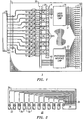
- the optical module 1of the invention consists of a semiconductor, ceramic or plastic substrate 2.
- a packaged laser array chip 4 consists of a plurality of surface or edge emitting lasers 5 operating at a predetermined wavelength such as 1310 nm.
- Laser array 4 is positioned in substrate 2 such that the streams of light that are emitted from the lasers 5 are parallel to and located substantially at the surface of substrate 2. To arrange the lasers at the surface of substrate 2, it may be necessary to photochemically or mechanically mill a hole in substrate 2 to receive the laser array 4.
- the hole may consist of a milled depression in the surface of substrate 2.
- Transmission elements 8 consisting of optical waveguides located within substrate 2 or fibers placed on substrate 2 connect each of the lasers 5 to the inputs of CWDM splitters 10.
- Electrical conductors 12 connect the lasers 5 of laser array 4 to controlling electrical elements such as a laser driver chip 16, framers or the like. These electrical elements are connected to the module's electrical connector 19 by conductors 21.
- the electrical elements are shown as being integrated onto the substrate 2, they can be located off of substrate 2 and on an associated device such as a line card circuit board if desired.
- a photodiode array 20 is shown consisting of a plurality of photodiodes 22 operating at a predetermined wavelength such as 1550 nm arranged in a row along one edge of chip 24.
- the number of photodiodes is equal to the number of lasers on laser array 4.
- Photodiodes 22 are connected to bonding pads 28 via conductors 30. Slots 32 are milled in the edge of chip 24 between the photodiodes 22 to create teeth or extending members 34 such that photodiode array 20 has a comb-like structure where the photodiodes are disposed in the teeth 34 of the "comb.”
- substrate 2 includes a plurality of mechanically or chemically milled apertures 38 for receiving the teeth 34 of photodiode array 20.
- Photodiode array 20 is inserted into substrate 2 such that teeth 34 extend into apertures 38 and are positioned such that the photodiodes 22 are disposed at the level of substrate 2 aligned with waveguides or fibers 40.
- Waveguides or fibers 40 extend to another input of CWDM couplers 10.
- Slots 32 of photodiode array 20 extend over and bridge the waveguides or fibers 8 emanating from lasers 5. Once the photodiode array 20 is properly aligned in substrate 2, it is bonded to the substrate.
- Bonding pads 28 are connected to conductors 42 that are connected to electrical elements such as photodiode preamplifier decision circuits 44, clock recovery circuits, framers or the like.
- the electrical elements 44 are connected to the module electrical connector 19 by conductors 23. Although the electrical elements are shown as being integrated onto the substrate 2, they can be located off of substrate 2 and on an associated device such as a line card circuit board if desired.
- CWDM couplers 10 function to combine and split the light as the light is transmitted between the separate fibers leading to the lasers 5 and photodiodes 22 and the single fibers 41 carrying the combined traffic from the optical module of the invention to the opposite end of the fiber link.
- the optical fibers or waveguides 41 are connected to an optical fiber ribbon 43 for transmitting the combined upstream and downstream traffic between the link endpoints.
- the optical module 1 is connected to a line card for use in a network element such as a switching system in a telecommunications network for providing fiber to the customer.
- a network element such as a switching system in a telecommunications network for providing fiber to the customer.
- FIG. 3 a typical subrack or shelf 50 and interface units such as line cards 52 for a switching system or other network element are shown. While specific reference is made to line cards 52, is to be understood that the optical module of the invention also can be used on trunk cards, other interface cards or other elements.
- Subrack 50 consists of side plates 54 and 56 and backplate 60 including electrical connectors 62, one connector 62 being provided for each of the line cards 52. Connectors 62 releasably engage connectors 64 on the line cards 52 to allow communication between the line card and the switching system or other network element.
- Line cards 52 consist of a circuit pack 65 having circuitry for controlling the lines hosted by that line card.
- a face place 66 is connected to the side of the circuit pack opposite to connector 64.
- Face plate 66 includes an aperture 68 through which the plug 72 of cable assembly 74 can access an optical connector 69 on the line card.
- the line card 52 is inserted into subrack 50 so that connector 64 engages the backplane connector 62 and latches 69 engage supports 58.
- Plug 72 is inserted through aperture 68 into engagement with the pin connectors to complete the physical installation of the line card.
- Cable assembly 74 provides a connection to the optical fibers that extends to the customer premise or other network element.
- line card 52 interfaces between the fiber transmission elements to the customer premise and the switching system or other network element hosting the line card as is generally known in the art.
- the optical module of the invention 1 is mounted on circuit pack 65 such that the optical waveguides or fibers extending from CWDM splitters terminate at optical connector 69.
- the waveguides or placed fibers could be connected directly to connector 69 or that other transmission techniques could be used.
- the optical module 1 communicates with downstream network elements such a customer premise equipment.
- the optical module's electrical connector 19 is electrically connected to the electronics on circuit pack 65 such that when circuit pack 65 is inserted in network element, the optical module 1 is in communication with the network element.
- the electronics such as the laser chip driver and photodiode interface chip can be located on circuit pack 65 rather than on the optical module 1.
- the optical module of the invention is relatively small, compact, and inexpensive it can be used to create high density interface cards. For example, to provide 24 channels, two of the 12 channel modules described with reference to FIGs. 1 and 2 are used. It will be appreciated that the number of channels provided and the number of modules used to provide those channels are a matter of engineering design choice. Moreover, because of its simple design, it eliminates the physical design problems of the prior art.
- the "comb" structure of the photodiode array allows the interdigitation of the photodiodes and lasers thereby greatly simplifying the construction of the CWDM couplers and eliminating the need for complex transmission arrangements.
- the photodiode array could be mounted to the substrate in place of the laser array and the lasers mounted on a "comb" shaped array such that the relative positions of the lasers and photodiodes are reversed from that in the illustrated example.
Landscapes
- Physics & Mathematics (AREA)
- General Physics & Mathematics (AREA)
- Optics & Photonics (AREA)
- Optical Couplings Of Light Guides (AREA)
- Optical Communication System (AREA)
- Photo Coupler, Interrupter, Optical-To-Optical Conversion Devices (AREA)
Claims (9)
- Optische Schnittstellenvorrichtung (1), umfassend ein erstes ebenes Substrat (2), das mehrere lichtemittierende Mittel (5) und erste optische Wellenleiter (8) auf dem ersten Substrat (2) und parallel zu einer Hauptoberfläche des letzteren zum jeweiligen Verbinden der lichtemittierenden Mittel (5) mit mehreren Optokopplern (10) trägt, ein zweites ebenes Substrat (24), welches mehrere lichtempfangende Mittel (22) trägt, wobei das zweite Substrat (24) an dem ersten Substrat (2) angebracht ist, derart, dass die ersten optischen Wellenleiter (8) und die mehreren lichtempfangenden Mittel (22) ineinandergreifen, und zweite optische Wellenleiter (40) auf dem ersten Substrat (2) und parallel zu einer Hauptoberfläche davon zum jeweiligen Verbinden der lichtempfangenden Mittel (22) mit den mehreren Optokopplern (10), wobei die optische Schnittstellenvorrichtung (1) DADURCH GEKENNZEICHNET IST, DASS:die Optokoppler (10) auf dem ersten Substrat (2) angeordnet sind,das zweite Substrat (24) senkrecht zur Ebene des ersten Substrats (2) angebracht ist, wobei die lichtempfangenden Mittel (22) auf dem zweiten Substrat (24) Licht empfangen, welches sich parallel zu der Hauptoberfläche des ersten Substrats (2) ausbreitet,das zweite Substrat (24) an dem ersten Substrat (2) derart angebracht ist, dass die lichtempfangenden Mittel (22) jeweils mit Endflächen der zweiten optischen Wellenleiter (40) optisch gekoppelt sind, wobei das Licht, welches durch die lichtemittierenden Mittel (5) erzeugt wird, mit einem Bestimmungsort außerhalb der optischen Schnittstellenvorrichtung (1), und Licht von außerhalb der optischen Schnittstellenvorrichtung (1), welches durch die Optokoppler (10) zu empfangen ist, sich in entgegengesetzte Richtungen auf bidirektionalen optischen Wellenleitern (41) fortpflanzt, wobei die Optokoppler (10) jeweils ausgebildet sind, um Licht von den ersten optischen Wellenleitern (8) zu den bidirektionalen optischen Wellenleitern (41) zu koppeln und um Licht von den bidirektionalen optischen Wellenleitern (41) zu den zweiten optischen Wellenleitern (40) zu koppeln.
- Optische Schnittstellenvorrichtung nach Anspruch 1, wobei die lichtemittierenden Mittel (5) eine Mehrzahl von Lasern (5) und die lichtempfangenden Mittel (2) mehrere Fotodioden (22) aufweisen.
- Vorrichtung nach Anspruch 1, wobei die ersten optischen Wellenleiter (8) entweder mehrere optische Wellenleiter, die im ersten Substrat (2) ausgebildet sind, oder mehrere Fasern, die auf dem ersten Substrat (2) angeordnet sind, aufweisen.
- Vorrichtung nach Anspruch 1 oder 3, wobei die zweiten optischen Wellenleiter (40) entweder andere mehrere optische Wellenleiter, die in dem ersten Substrat (2) ausgebildet sind, oder andere mehrere Fasern, die in dem ersten Substrat (2) angeordnet sind, aufweisen.
- Vorrichtung nach Anspruch 1, wobei die ersten optischen Wellenleiter (8) entweder mehrere Fasern aufweisen, die an dem ersten Substrat (2) angeordnet sind, und die zweiten optischen Wellenleiter (40) andere mehrere Fasern aufweisen, die an dem ersten Substrat (2) angeordnet sind und mit den mehreren Fasern ineinandergreifen, oder mehrere Wellenleiter, die in dem ersten Substrat (2) ausgebildet sind, und die zweiten optischen Wellenleiter (40) andere mehrere Wellenleiter, die in dem ersten Substrat (2) ausgebildet sind und mit den mehreren Wellenleitern ineinandergreifen, aufweisen.
- Vorrichtung nach Anspruch 1, 2, 3 oder 4, wobei das zweite Substrat (24) eine Mehrzahl von Ausnehmungen (32) aufweist, die entlang einer Kante davon ausgebildet sind, um mehrere vorragende Glieder (34) vorzusehen, wobei jeweils eines der mehreren lichtempfangenden Mittel (22) in jedem der vorragenden Glieder (34) angeordnet ist, wobei das zweite Substrat (24) an dem ersten Substrat (2) derart befestigt ist, dass die vorragenden Glieder (34) zwischen den ersten optischen Wellenleitern (8), die Licht von dem anderen der lichtempfangenden (22) bzw. -emittierenden (5) Mittel führen, angeordnet sind.
- Vorrichtung nach Anspruch 6, wobei das erste Substrat (2) Abschnitte umfasst, welche mehrere Öffnungen (38) bilden, wobei die Öffnungen (38) zwischen den ersten optischen Wellenleitern (8) und den vorragenden Gliedern (34) angeordnet sind und die Öffnungen (38) einen Abschnitt der jeweiligen vorragenden Glieder (34) darin aufnehmen.
- Vorrichtung nach Anspruch 1, wobei das erste Substrat (2) an einer Leitungskarte (52) in einem Telekommunikationsnetzelement angebracht ist.
- Vorrichtung nach Anspruch 1, ferner umfassend:ein Schaltkreismodul (65), an welchem das erste Substrat (2) angebracht ist;einen Verbinder (64), der an dem Schaltkreismodul (65) angebracht und ausgebildet ist, um externe elektrische Pfade für Signale bereitzustellen, welche den lichtemittierenden Mitteln (5) und den lichtempfangenden Mitteln (22) zugeordnet sind, undeinen Verbinder (69), der an dem Schaltkreismodul (65) angebracht und ausgebildet ist, um externe optische Pfade für Lichtstrahlen bereitzustellen, welche den lichtemittierenden Mitteln (5) und den lichtempfangenden Mitteln (22) zugeordnet sind.
Applications Claiming Priority (2)
| Application Number | Priority Date | Filing Date | Title |
|---|---|---|---|
| US915244 | 1997-08-20 | ||
| US08/915,244 US5943456A (en) | 1997-08-20 | 1997-08-20 | Coarse wavelength division multiplexing optical system |
Publications (2)
| Publication Number | Publication Date |
|---|---|
| EP0903601A1 EP0903601A1 (de) | 1999-03-24 |
| EP0903601B1 true EP0903601B1 (de) | 2006-10-04 |
Family
ID=25435446
Family Applications (1)
| Application Number | Title | Priority Date | Filing Date |
|---|---|---|---|
| EP98306392A Expired - Lifetime EP0903601B1 (de) | 1997-08-20 | 1998-08-11 | Mehrkanaliges optisches Empfänger-/Sendersystem |
Country Status (4)
| Country | Link |
|---|---|
| US (1) | US5943456A (de) |
| EP (1) | EP0903601B1 (de) |
| JP (1) | JP3489722B2 (de) |
| DE (1) | DE69836058T2 (de) |
Families Citing this family (25)
| Publication number | Priority date | Publication date | Assignee | Title |
|---|---|---|---|---|
| JPS57181801A (en) * | 1981-05-01 | 1982-11-09 | Uichi Miyawaki | Saw and manufacture of saw |
| US20010048793A1 (en) * | 1999-05-27 | 2001-12-06 | Edwin Dair | Method and apparatus for multiboard fiber optic modules and fiber optic module arrays |
| US6527456B1 (en) | 1999-10-13 | 2003-03-04 | Teraconnect, Inc. | Cluster integration approach to optical transceiver arrays and fiber bundles |
| GB0016500D0 (en) * | 2000-07-06 | 2000-08-23 | Pace Micro Tech Plc | Control and communication system for components of electrical apparatus |
| US20020131125A1 (en) * | 2001-03-16 | 2002-09-19 | Myers Michael H. | Replicated-spectrum photonic transceiving |
| US20020131100A1 (en) * | 2001-03-16 | 2002-09-19 | Myers Michael H. | Method for photonic wavelength error detection |
| US6542306B2 (en) | 2001-03-16 | 2003-04-01 | Optical Coating Laboratories, Inc. | Compact multiple channel multiplexer/demultiplexer devices |
| US6407846B1 (en) | 2001-03-16 | 2002-06-18 | All Optical Networks, Inc. | Photonic wavelength shifting method |
| US6775431B1 (en) * | 2001-04-18 | 2004-08-10 | Turin Networks | V groove optic switch |
| US6636658B2 (en) | 2001-04-23 | 2003-10-21 | Optical Coating Laboratory, Inc. | Wavelength division multiplexing/demultiplexing systems |
| CN1541461A (zh) * | 2001-07-13 | 2004-10-27 | ʽϵͳ�ɷݹ�˾ | 光学系统和光学系统中的方法 |
| US6769812B1 (en) | 2002-07-01 | 2004-08-03 | Nortel Networks, Ltd | Method and apparatus for forming an optical module with optical and electrical connections facing one direction |
| US6796716B1 (en) * | 2002-07-01 | 2004-09-28 | Nortel Networks, Ltd. | Network device containing an optical module having optical and electrical connections facing one direction |
| US7106973B2 (en) * | 2002-08-13 | 2006-09-12 | Lightpointe Communications, Inc. | Apparatus and method for use in free-space optical communication comprising optically aligned components integrated on circuit boards |
| US20040120717A1 (en) * | 2002-12-18 | 2004-06-24 | Lightpointe Communications, Inc. | Extended source free-space optical communication system |
| US7636522B2 (en) * | 2004-04-15 | 2009-12-22 | Infinera Corporation | Coolerless photonic integrated circuits (PICs) for WDM transmission networks and PICs operable with a floating signal channel grid changing with temperature but with fixed channel spacing in the floating grid |
| JP2005341118A (ja) * | 2004-05-26 | 2005-12-08 | Hitachi Communication Technologies Ltd | フィルタ回路、論理ic、マルチチップモジュール、フィルタ搭載型コネクタ、伝送装置及び伝送システム |
| CN101278217B (zh) * | 2005-06-30 | 2012-03-21 | 英飞聂拉股份有限公司 | 用于多通道光子集成电路(pic)的波长锁定和功率控制系统 |
| US7559703B2 (en) * | 2005-09-14 | 2009-07-14 | Ibiden Co., Ltd. | Optical module and data communication system including the optical module |
| USD591745S1 (en) * | 2005-09-19 | 2009-05-05 | Schweitzer Engineering Laboratories, Inc. | Data stream management device |
| KR100765466B1 (ko) | 2006-02-28 | 2007-10-09 | 한국광기술원 | 박막간섭형 채널소자의 다중병렬 배치구조를 갖는 cwdm광모듈 |
| JP4343238B2 (ja) * | 2007-05-29 | 2009-10-14 | 日本航空電子工業株式会社 | 組立体 |
| US9215517B2 (en) * | 2012-11-15 | 2015-12-15 | Compass Electro Optical Systems Ltd. | Switching Clos network universal element |
| US9961799B1 (en) * | 2016-08-19 | 2018-05-01 | Juniper Networks, Inc. | Apparatuses and systems for increasing thermal mass in line card heatsinks |
| CN110265876B (zh) * | 2019-06-21 | 2021-02-12 | 中国科学院半导体研究所 | 基于低温共烧陶瓷的光电集成封装结构 |
Citations (1)
| Publication number | Priority date | Publication date | Assignee | Title |
|---|---|---|---|---|
| DE4411860A1 (de) * | 1994-04-06 | 1995-10-19 | Fraunhofer Ges Forschung | Dreidimensionale Wellenleiterstrukturen und Verfahren zu ihrer Herstellung |
Family Cites Families (8)
| Publication number | Priority date | Publication date | Assignee | Title |
|---|---|---|---|---|
| JPS6067907A (ja) * | 1983-09-26 | 1985-04-18 | Hitachi Ltd | 光電変換モジユ−ル |
| JPS62159105A (ja) * | 1986-01-08 | 1987-07-15 | Hitachi Ltd | 双方向伝送用光モジユ−ル |
| US4943136A (en) * | 1988-12-09 | 1990-07-24 | The Boeing Company | Optical backplane interconnection |
| KR100225026B1 (ko) * | 1993-03-31 | 1999-10-15 | 구라우치 노리타카 | 광파이버어레이 |
| US5345524A (en) * | 1993-05-20 | 1994-09-06 | Motorola, Inc. | Optoelectronic transceiver sub-module and method for making |
| US5394489A (en) * | 1993-07-27 | 1995-02-28 | At&T Corp. | Wavelength division multiplexed optical communication transmitters |
| JP2859112B2 (ja) * | 1993-11-26 | 1999-02-17 | 日本電気 株式会社 | 発光アレーモジュール |
| US5745270A (en) * | 1996-03-28 | 1998-04-28 | Lucent Technologies Inc. | Method and apparatus for monitoring and correcting individual wavelength channel parameters in a multi-channel wavelength division multiplexer system |
-
1997
- 1997-08-20 US US08/915,244 patent/US5943456A/en not_active Expired - Lifetime
-
1998
- 1998-08-11 DE DE69836058T patent/DE69836058T2/de not_active Expired - Fee Related
- 1998-08-11 EP EP98306392A patent/EP0903601B1/de not_active Expired - Lifetime
- 1998-08-20 JP JP23339798A patent/JP3489722B2/ja not_active Expired - Fee Related
Patent Citations (1)
| Publication number | Priority date | Publication date | Assignee | Title |
|---|---|---|---|---|
| DE4411860A1 (de) * | 1994-04-06 | 1995-10-19 | Fraunhofer Ges Forschung | Dreidimensionale Wellenleiterstrukturen und Verfahren zu ihrer Herstellung |
Also Published As
| Publication number | Publication date |
|---|---|
| US5943456A (en) | 1999-08-24 |
| JP3489722B2 (ja) | 2004-01-26 |
| DE69836058D1 (de) | 2006-11-16 |
| EP0903601A1 (de) | 1999-03-24 |
| DE69836058T2 (de) | 2007-04-05 |
| JPH11163389A (ja) | 1999-06-18 |
Similar Documents
| Publication | Publication Date | Title |
|---|---|---|
| EP0903601B1 (de) | Mehrkanaliges optisches Empfänger-/Sendersystem | |
| US6661940B2 (en) | Apparatus and method for rebroadcasting signals in an optical backplane bus system | |
| KR100570424B1 (ko) | 광학적으로 접속가능한 회로 보드 | |
| US4943136A (en) | Optical backplane interconnection | |
| US7447440B2 (en) | Multiple channel optical transceiver modules | |
| US7275876B2 (en) | Optical transmission circuit device | |
| US5313536A (en) | Modular photonic waveguide distribution system | |
| JPH10123373A (ja) | 導波路型光モジュール | |
| US5066097A (en) | Connector for an optical cable | |
| EP1811324A2 (de) | Optischer Schalter mit zueinander senkrecht angeordneten planaren Lichtwellenleiterschaltkreisen | |
| US5091985A (en) | Optical signal connection device for units to be inserted in a rack | |
| US6625369B1 (en) | Optical transmitter-receiver module | |
| KR0135410B1 (ko) | 광접속장치 | |
| KR101501140B1 (ko) | 광 파워 모니터 구조를 개량시킨 평판형 광도파로 소자 모듈 | |
| US7587115B1 (en) | Integrated functionality in optical backplane | |
| US6128428A (en) | Single-type array optical conversion apparatus | |
| GB2237949A (en) | Optical networks | |
| JPS5915422B2 (ja) | パツケ−ジ間光伝送方式 | |
| JP2002044849A (ja) | 光電気複合実装構造 | |
| KR0174407B1 (ko) | 인쇄회로기판의 광신호 상호연결장치 | |
| Chamberlain et al. | Topologies and technologies for optically interconnected multicomputers using inverted graphs | |
| TW202542567A (zh) | 用於高密度光纖連接之裝置、系統及方法 | |
| CN118033824A (zh) | 光连接器、光尾纤、光跳线、光通信设备及系统 | |
| KR100359942B1 (ko) | 광 스위치 | |
| KR100606697B1 (ko) | 광섬유 결합기를 이용한 가변광감쇠기 |
Legal Events
| Date | Code | Title | Description |
|---|---|---|---|
| PUAI | Public reference made under article 153(3) epc to a published international application that has entered the european phase |
Free format text: ORIGINAL CODE: 0009012 |
|
| AK | Designated contracting states |
Kind code of ref document: A1 Designated state(s): DE FR GB |
|
| AX | Request for extension of the european patent |
Free format text: AL;LT;LV;MK;RO;SI |
|
| 17P | Request for examination filed |
Effective date: 19990910 |
|
| AKX | Designation fees paid |
Free format text: DE FR GB |
|
| 17Q | First examination report despatched |
Effective date: 20041028 |
|
| GRAP | Despatch of communication of intention to grant a patent |
Free format text: ORIGINAL CODE: EPIDOSNIGR1 |
|
| RTI1 | Title (correction) |
Free format text: MULTI-CHANNEL OPTICAL RECEIVER/TRANSMITTER SYSTEM |
|
| GRAS | Grant fee paid |
Free format text: ORIGINAL CODE: EPIDOSNIGR3 |
|
| GRAA | (expected) grant |
Free format text: ORIGINAL CODE: 0009210 |
|
| AK | Designated contracting states |
Kind code of ref document: B1 Designated state(s): DE FR GB |
|
| REG | Reference to a national code |
Ref country code: GB Ref legal event code: FG4D |
|
| REF | Corresponds to: |
Ref document number: 69836058 Country of ref document: DE Date of ref document: 20061116 Kind code of ref document: P |
|
| ET | Fr: translation filed | ||
| PLBE | No opposition filed within time limit |
Free format text: ORIGINAL CODE: 0009261 |
|
| STAA | Information on the status of an ep patent application or granted ep patent |
Free format text: STATUS: NO OPPOSITION FILED WITHIN TIME LIMIT |
|
| 26N | No opposition filed |
Effective date: 20070705 |
|
| PGFP | Annual fee paid to national office [announced via postgrant information from national office to epo] |
Ref country code: DE Payment date: 20080822 Year of fee payment: 11 |
|
| PGFP | Annual fee paid to national office [announced via postgrant information from national office to epo] |
Ref country code: FR Payment date: 20080813 Year of fee payment: 11 |
|
| PGFP | Annual fee paid to national office [announced via postgrant information from national office to epo] |
Ref country code: GB Payment date: 20080821 Year of fee payment: 11 |
|
| GBPC | Gb: european patent ceased through non-payment of renewal fee |
Effective date: 20090811 |
|
| REG | Reference to a national code |
Ref country code: FR Ref legal event code: ST Effective date: 20100430 |
|
| PG25 | Lapsed in a contracting state [announced via postgrant information from national office to epo] |
Ref country code: FR Free format text: LAPSE BECAUSE OF NON-PAYMENT OF DUE FEES Effective date: 20090831 Ref country code: DE Free format text: LAPSE BECAUSE OF NON-PAYMENT OF DUE FEES Effective date: 20100302 |
|
| PG25 | Lapsed in a contracting state [announced via postgrant information from national office to epo] |
Ref country code: GB Free format text: LAPSE BECAUSE OF NON-PAYMENT OF DUE FEES Effective date: 20090811 |