EP0903564A2 - Circuit à haute température de detection de photocourant à deux fils - Google Patents
Circuit à haute température de detection de photocourant à deux fils Download PDFInfo
- Publication number
- EP0903564A2 EP0903564A2 EP98307611A EP98307611A EP0903564A2 EP 0903564 A2 EP0903564 A2 EP 0903564A2 EP 98307611 A EP98307611 A EP 98307611A EP 98307611 A EP98307611 A EP 98307611A EP 0903564 A2 EP0903564 A2 EP 0903564A2
- Authority
- EP
- European Patent Office
- Prior art keywords
- photocurrent
- current
- detector circuit
- driver
- transimpedance amplifier
- Prior art date
- Legal status (The legal status is an assumption and is not a legal conclusion. Google has not performed a legal analysis and makes no representation as to the accuracy of the status listed.)
- Withdrawn
Links
Images
Classifications
-
- G—PHYSICS
- G01—MEASURING; TESTING
- G01J—MEASUREMENT OF INTENSITY, VELOCITY, SPECTRAL CONTENT, POLARISATION, PHASE OR PULSE CHARACTERISTICS OF INFRARED, VISIBLE OR ULTRAVIOLET LIGHT; COLORIMETRY; RADIATION PYROMETRY
- G01J1/00—Photometry, e.g. photographic exposure meter
- G01J1/42—Photometry, e.g. photographic exposure meter using electric radiation detectors
- G01J1/44—Electric circuits
-
- G—PHYSICS
- G01—MEASURING; TESTING
- G01J—MEASUREMENT OF INTENSITY, VELOCITY, SPECTRAL CONTENT, POLARISATION, PHASE OR PULSE CHARACTERISTICS OF INFRARED, VISIBLE OR ULTRAVIOLET LIGHT; COLORIMETRY; RADIATION PYROMETRY
- G01J1/00—Photometry, e.g. photographic exposure meter
- G01J1/42—Photometry, e.g. photographic exposure meter using electric radiation detectors
- G01J1/429—Photometry, e.g. photographic exposure meter using electric radiation detectors applied to measurement of ultraviolet light
Definitions
- This invention relates to a photocurrent sensor circuit, and more particularly, to a two-wire photocurrent sensor circuit.
- Gas turbine flame intensity may be measured and utilized in the gas turbine engine for efficient operation.
- the flame in a gas turbine engine generates electromagnetic emissions in the visible, infrared, and the ultra-violet electromagnetic spectrum. Ultra-violet emissions of particular interest occur in the range from about 200 to about 400 nano-meters.
- the silicon-carbide photocurrent sensor has demonstrated it's ability to respond well to ultra-violet emissions in a background of infrared emissions and visible emissions, while being relatively insensitive to the infrared and visible emissions, as is disclosed in U.S. Patent No. 5,394,005.
- a five-wire photocurrent detector circuit is disclosed in U.S. Patent No. 5,589,682, hereinafter identified as Patent '682, which describes a silicon-carbide photocurrent detector.
- Patent '682 discloses a photocurrent detector circuit coupled to five wires, each wire having one of the following functions: positive power supply coupling; negative power supply coupling; ground coupling; and couplings for each of two output signals. It is advantageous to minimize the number of wires in gas turbine so as to reduce the complexity, cost, and maintenance. It is thus desirable to employ a silicon-carbide photocurrent detector circuit capable of operating effectively with as few connections as possible.
- a gas turbine engine typically operates over a wide temperature range.
- the flame generated by the gas turbine engine typically generates temperatures above 2000 degrees Centigrade (C).
- Hot sections aft of the combustor of a gas turbine may be heated to 300°C. It is desirable to employ a photocurrent detection circuit that will measure photocurrent accurately at temperatures up to 300 ° C.
- Reducing the number of components in a photocurrent detection circuit provides potential cost and reliability benefits, making it desirable to employ a photocurrent detector circuit employing as few components as necessary.
- a photocurrent detector circuit coupled to a voltage source and an indicator for converting a photocurrent within a photocurrent sensor into a supply current comprising:
- a photocurrent detector circuit coupled to a voltage source and an indicator for converting a photocurrent within a photocurrent sensor into a supply current comprising:
- a high reliability photocurrent sensor circuit may be utilized for detecting photocurrent corresponding with ultra-violet emissions in a range of about 200 to about 400 nano-meters.
- the photocurrent detector circuit may be operational over a temperature range from about 25 degrees Centigrade to about 300 degrees Centigrade.
- the photocurrent detector circuit may provide a flame intensity current signal in correspondence with the flame intensity of a turbine engine.
- the flame intensity current signal may be combined with the supply current in the two photocurrent detector power supply wires so that an external current detector can measure the flame intensity.
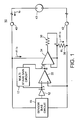
- Figure 1 is a schematic block diagram of the present invention.
- Figure 2 is a schematic diagram of one embodiment of the present invention.
- FIG. 3 is a schematic diagram showing further details of one embodiment of the present invention.
- Photocurrent detector circuit 50 detects a portion of the ultra-violet emissions being emitted from a flame in a gas turbine engine and generates a photocurrent in correspondence with the detected energy in the ultra-violet wavelength as sensed by a silicon-carbide based photocurrent sensor 12.
- the photocurrent generated by photocurrent sensor 12 is then amplified and electrically coupled to the output of photocurrent detector circuit 50 in which a supply current (I o ) is generated that is proportional to the gas turbine flame intensity.
- Patent '682 discloses a circuit having a clamping function and providing inverting and non-inverting outputs. To reduce the number of components and the number of output wires in a photocurrent detector it is desirable to employ a circuit which eliminates the clamping function, and eliminates the inverting and non-inverting functions disclosed in Patent '682.
- the present invention accomplishes the above stated reduction in components and substitute functionality by employing a transimpedance amplifier 21, comprising an operational amplifier 22, a multi-stage gain circuit 17, and a current driver 34, as is further discussed below.
- Photocurrent detection circuit 50 employs transimpedance amplifier 21 to provide precise amplification of the photocurrent signal generated by photocurrent sensor 12 by establishing multi-levels of gain that prevent the UV emission signal of transimpedance amplifier 21 from going beyond its operational limit, thus eliminating the need for the clamping circuit disclosed in Patent '682.
- the gain of transimpedance amplifier 21 is hereinafter defined as the output voltage per unit input current.
- photocurrent detection circuit 50 employs current driver 34 to generate a variable driver current 41 (I c ) which is proportional to the supply current (I o ) that flows through a source voltage 43 from a positive source voltage terminal 40 to a negative source voltage terminal 42.
- Supply current (1,,) thus provides an output signal that is distinct from the inverting and non-inverting output functions disclosed in Patent '682.
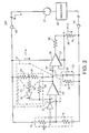
- Photocurrent detector circuit 100 illustrated in Figure 2 is one embodiment further illustrating photocurrent detector circuit 50 as depicted in the schematic block diagram of Figure 1.
- Photocurrent detector circuit 100 comprises the following additional elements: a bias voltage circuit 23; a multi-stage gain circuit 17; a filter circuit 32; a sensor bias circuit 15; a negative driver amplifier terminal 37, and a positive driver amplifier terminal 38.
- Sensor bias circuit 15 comprises a first photocurrent sensor bias resistor 10 and a second photocurrent sensor bias resistor 14 .
- Bias voltage circuit 23 comprises: a low gain resistor 18; a first low gain bias resistor 24; and a second low gain bias resistor 26.
- Multi-stage gain circuit 17 comprises: a diode 16; a high gain resistor 20; and bias voltage circuit 23.
- Photocurrent detector circuit 100 is interconnected as illustrated in the schematic diagram in Figure 2.
- photocurrent detector circuit 100 The function of elements in photocurrent detector circuit 100 are discussed next including: photocurrent sensor 12; photocurrent sensor bias circuit 15; operational amplifier 22; multistage gain circuit 17; filter circuit 32; and driver amplifier 34.
- Photocurrent sensor 12 is disposed in a gas turbine engine such that a portion of the ultra-violet emissions from the gas turbine engine flame is detected by photocurrent sensor 12. As ultraviolet emissions are generated by the flame of the gas turbine engine, a proportional photocurrent is generated in photocurrent sensor 12. Typically, photocurrent sensor 12 generates a photocurrent in the order of magnitude of nano-amps. The magnitude of photocurrent generated by photocurrent sensor 12 directly corresponds with the magnitude of ultra-violet (UV) emissions produced by the jet engine flame-especially UV emissions in the range of about 200 to about 400 nano-meters, with a peak sensitivity of about 270 nano-meters.
- UV ultra-violet
- Detector circuit 100 ( Figure 2) employs sensor bias circuit 15 which generates a bias voltage that is applied at the negative input of operational amplifier 22 so as to cause detector circuit 100 to provide a minimal driver current 41 (I c ) generated by current driver 34.
- This bias voltage is selected to generate a bias current greater than the maximum current drawn by photocurrent detector circuit 100.
- maximum supply current (I B ) is typically about seven milli-amps at 300°C, and is generated based on a bias voltage of about one volt across first photocurrent sensor bias resistor 10.
- Transimpedance amplifier 21 converts the photocurrent generated by photocurrent sensor 12 into an UV emission signal. At least two transimpedance gain values may be required because the current generated by photocurrent sensor has a large dynamic range. In this Specification transimpedance amplifier 21 is described as having two values of gain; any number of values of gain, however, may be employed so as to compensate for the sensitivity of a different photocurrent sensor having a unique response characteristic.
- Operational amplifier 22 is selected because the input impedance of this amplifier circuit is much lower than the impedance from external elements in photocurrent detection circuit 100 coupled directly to the input at point "F". Additionally, the output impedance of transimpedance amplifier 21 is much lower than the impedance from external elements directly coupled to the output at point "B".
- transimpedance amplifier 21 enables a UV emission signal to be generated which is proportional to the photocurrent at point "F.” Additionally, the use of transimpedance amplifier 21 enables the input current to be substantially unaffected by the impedance from external elements at point "F.” Finally, the use of transimpedance amplifier 21 enables the UV emission signal to be substantially unaffected by the impedance of extemal elements directly coupled to transimpedance amplifier 21 at point "B.”
- One embodiment of multi-stage gain circuit 17 is a resistance network comprising diode 16; low gain resistor 18; high gain resistor 20; first low gain bias resistor 24; and second low gain bias resistor 26.
- Diode 16 is biased by voltage bias circuit 23 so that it is reverse biased.
- the voltage bias level is set by selecting a first and second low gain bias resistor to provide a predetermined voltage level at point "E.”
- the voltage bias level is set so that transimpedance amplifier 21 is not saturated when the photocurrent is at a maximum level.
- Diode 16 is forward biased when the photocurrent level is in the upper range thereby reducing the transimpedance at high photocurrent levels.
- the net effect when diode 16 is forward biased is to reduce the feedback impedance.
- This reduction in feedback impedance reduces the transimpedance of amplifier 21; as such, the voltage output of transimpedance amplifier 21 is lower when diode 16 is reverse biased.
- the gain of transimpedance amplifier 21 is respectively 2 x10 9 when diode 16 is reverse biased and 2 x10 7 when diode 16 is forward biased.
- the predetermined bias voltage is typically about 1/3 of the full range of the output voltage of transimpedance amplifier 21.
- Filter circuit 32 filters the UV emission signal of transimpedance amplifier 21.
- the point at which filter circuit 32 is active is determined by the combination selected between filter capacitor 28 and filter resistor 30.
- Filter circuit 32 is an RC filter. Filter circuit 32 thus filters undesirable high frequency noise at point "B".
- 1000 Hertz noise is filtered at the output of transimpedance amplifier 21; any other filter frequency however, may be selected.
- Filter circuit 32 also severs to stabilize detector circuit 100.
- Current driver 34 controls driver current 41. As the output voltage of current driver 34 rises the voltage at point “A” rises by a proportional amount. Thus, as UV emission signal at point “B” changes the voltage at point “A” correspondingly changes by “substantially the same” percentage. The percentage change defining what is “substantially the same” at point “A” and point “B” is determined by the level of common mode rejection of driver amplifier 34. Driver amplifier 34 is selected so that the common mode rejection enables the difference in voltage at point "A” and point “B” to be a negligible factor in the operation of photocurrent detector circuit 100.
- the voltage at point "A” controls the current flowing through output current load resistor 39, as defined by equation (1), where I c is driver current 41, V B is the input voltage of current amplifier 34, and R L is the resistance of load resistor 39.
- I c V B /R L
- the current I c flowing through output current load resistor 39 is substantially the same as the supply current I o flowing from positive supply voltage terminal 40 to negative supply voltage terminal 42.
- the difference between driver current I c and supply current I o flowing from positive supply voltage terminal 40 is the current flowing through other components of photocurrent detector circuit 100.
- driver current I c is above 99 percent of supply current I o . It should be noted that since the voltage at negative amplifier terminal 37 of current driver 34 is the same voltage as at point "A", consequently, current driver 34 floats at the voltage level of point "A".
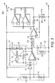
- photocurrent detector circuit 200 depicted in Figure 3.
- the primary difference between photocurrent detector circuit 100 and more detailed photocurrent detector circuit 200 is the number of current drivers.
- the number of current drivers has been increased to generate more driver current 41(I c ).
- Detailed photocurrent detector circuit 200 comprises the following additional components: a driver amplifier input resistor 110; a first output current control resistor 116; a second output current control resistor 120; and voltage followers 122.
- the currents generated by voltage followers 122 are summed at point "A”.
- Driver current 41 (I c ) then flows through output current load resistor 39.
- driver current 41 (I c ) flowing through output current load resistor 39 and associated source current I o flowing from positive supply voltage terminal 40 is substantially the same as discussed above. Since the voltage at point “B” is “substantially the same “ as the voltage level at point “A” voltage followers 122 track current driver 34, and the respective current generated voltage followers 122 is summed at point "A".
- Table 1 illustrates several columns of supply current (I o ) measurements of photocurrent detector circuit 200 at temperatures from 25° C to 300° C.
- the first column is a list of values representing "Light" intensities from 1 to 0.
- the second column is a list of measurements of supply current I o minus baseline current I B at about 25° C.
- the third column is a list of measurements of supply current I o minus baseline current I B at about 300° C.
- supply current I o minus baseline current I B is approximately twelve milli-amps and drops to about zero milli-amps respectively.
- a similar observation of the present invention is also true at the 300 C level.
- supply current I o minus baseline current I B is approximately eight milli-amps and drops to about 0.02 milli-amps respectively.
- Supply Current Versus Ultra-violet Level over Temperature (I B 8.27 milli-amps and I o is supply current) All currents are illustrated in milli-amps "Light" I o -I B (25 C) I o -I B (300 C) 1.00 12.36 8.02 0.93 12.20 7.84 0.71 11.36 7.44 0.50 8.95 6.93 0.32 6.39 6.04 0.16 3.48 3.61 0.10 2.36 2.48 0.00 0.00 0.02
- Photocurrent detector circuit 100 generates supply current I o flowing from positive supply voltage terminal 40 to negative supply voltage terminal 42 that is proportional to the ultra-violet emissions produced by the gas turbine engine flame.
- Voltage source 43 provides supply voltage through positive supply voltage terminal 40 and negative supply voltage terminal to photocurrent detector circuit 100. Thus, only two wires are utilized in providing source voltage to photocurrent detector circuit 100 and an output signal as represented by supply current I o .
Landscapes
- Physics & Mathematics (AREA)
- General Physics & Mathematics (AREA)
- Spectroscopy & Molecular Physics (AREA)
- Photometry And Measurement Of Optical Pulse Characteristics (AREA)
- Amplifiers (AREA)
Applications Claiming Priority (2)
| Application Number | Priority Date | Filing Date | Title |
|---|---|---|---|
| US933897 | 1997-09-19 | ||
| US08/933,897 US5955734A (en) | 1997-09-19 | 1997-09-19 | High temperature two-wire photocurrent detector circuit |
Publications (2)
| Publication Number | Publication Date |
|---|---|
| EP0903564A2 true EP0903564A2 (fr) | 1999-03-24 |
| EP0903564A3 EP0903564A3 (fr) | 2000-05-24 |
Family
ID=25464663
Family Applications (1)
| Application Number | Title | Priority Date | Filing Date |
|---|---|---|---|
| EP98307611A Withdrawn EP0903564A3 (fr) | 1997-09-19 | 1998-09-18 | Circuit à haute température de detection de photocourant à deux fils |
Country Status (3)
| Country | Link |
|---|---|
| US (1) | US5955734A (fr) |
| EP (1) | EP0903564A3 (fr) |
| JP (1) | JPH11153484A (fr) |
Families Citing this family (3)
| Publication number | Priority date | Publication date | Assignee | Title |
|---|---|---|---|---|
| US7349128B2 (en) * | 2003-02-24 | 2008-03-25 | Kabushiki Kaisha Toshiba | Image scanner and peak detecting processing method of image scanner |
| CA2788225C (fr) * | 2009-10-09 | 2018-01-16 | Dh Technologies Development Pte. Ltd. | Appareil de mesure de tension rf d'un quadripole dans un spectrometre de masse |
| JP6889082B2 (ja) * | 2017-09-29 | 2021-06-18 | アズビル株式会社 | 火炎センサの駆動回路 |
Citations (1)
| Publication number | Priority date | Publication date | Assignee | Title |
|---|---|---|---|---|
| US5170035A (en) * | 1990-11-28 | 1992-12-08 | Webster Lee R | Sensor circuit for controlling flow in an instrument loop |
Family Cites Families (4)
| Publication number | Priority date | Publication date | Assignee | Title |
|---|---|---|---|---|
| US5287340A (en) * | 1992-02-13 | 1994-02-15 | International Business Machines Corporation | Differential amplifier for optical detectors in an optical data storage system |
| US5394005A (en) * | 1992-05-05 | 1995-02-28 | General Electric Company | Silicon carbide photodiode with improved short wavelength response and very low leakage current |
| US5589682A (en) * | 1995-06-07 | 1996-12-31 | General Electric Company | Photocurrent detector circuit with high sensitivity, fast response time, and large dynamic range |
| US5592124A (en) * | 1995-06-26 | 1997-01-07 | Burr-Brown Corporation | Integrated photodiode/transimpedance amplifier |
-
1997
- 1997-09-19 US US08/933,897 patent/US5955734A/en not_active Expired - Fee Related
-
1998
- 1998-09-07 JP JP10252066A patent/JPH11153484A/ja not_active Withdrawn
- 1998-09-18 EP EP98307611A patent/EP0903564A3/fr not_active Withdrawn
Patent Citations (1)
| Publication number | Priority date | Publication date | Assignee | Title |
|---|---|---|---|---|
| US5170035A (en) * | 1990-11-28 | 1992-12-08 | Webster Lee R | Sensor circuit for controlling flow in an instrument loop |
Also Published As
| Publication number | Publication date |
|---|---|
| EP0903564A3 (fr) | 2000-05-24 |
| US5955734A (en) | 1999-09-21 |
| JPH11153484A (ja) | 1999-06-08 |
Similar Documents
| Publication | Publication Date | Title |
|---|---|---|
| US4578583A (en) | Solid state ultraviolet flame detector | |
| US5936231A (en) | Photoelectric sensor circuit comprising an auxiliary photodiode and a current mirror circuit | |
| US7265333B2 (en) | Light-receiving circuit | |
| US20030178552A1 (en) | High dynamic range optical signal receiver | |
| US5955726A (en) | System for automatically sensing light in a predetermined range and correcting a meter luminance | |
| JP2005265846A (ja) | 暗光電流をキャンセルするカラーセンサ | |
| KR20190141077A (ko) | 전자 어셈블리, 전자 어셈블리를 포함하는 광학 가스 센서 및 전자 어셈블리를 이용하여 광전류 및 온도를 결합하여 측정하는 방법 | |
| US5880827A (en) | Measurement System with large dynamic range | |
| KR101131710B1 (ko) | 색상 감지기 및 집적 회로 칩 | |
| US5245196A (en) | Infrared flame sensor responsive to infrared radiation | |
| US6404342B1 (en) | Flame detector using filtering of ultraviolet radiation flicker | |
| US5955734A (en) | High temperature two-wire photocurrent detector circuit | |
| JPS6234169B2 (fr) | ||
| US5536934A (en) | Light intensity deterioration detecting circuit with compensation for resistance errors | |
| US5821528A (en) | Two light intensities difference convert into frequency modulator for parallel photodiodes | |
| US4471323A (en) | Protection circuits for complementary direct-coupled amplifiers | |
| JP2674110B2 (ja) | アバランシエホトダイオードのバイアス回路の温度補償回路 | |
| EP4571190A1 (fr) | Dispositif de surveillance, appareil de combustion et procédé d'amplification de signal | |
| JP2511730B2 (ja) | 火炎検出器 | |
| JP2543612B2 (ja) | 受光装置 | |
| JPS6128334B2 (fr) | ||
| JPS6276329A (ja) | 光受信回路 | |
| JPH02164226A (ja) | 受光素子保護回路 | |
| US5029278A (en) | Transducer interface circuit | |
| JPH06104660A (ja) | 交流増幅回路 |
Legal Events
| Date | Code | Title | Description |
|---|---|---|---|
| PUAI | Public reference made under article 153(3) epc to a published international application that has entered the european phase |
Free format text: ORIGINAL CODE: 0009012 |
|
| AK | Designated contracting states |
Kind code of ref document: A2 Designated state(s): DE FR GB IT |
|
| AX | Request for extension of the european patent |
Free format text: AL;LT;LV;MK;RO;SI |
|
| PUAL | Search report despatched |
Free format text: ORIGINAL CODE: 0009013 |
|
| AK | Designated contracting states |
Kind code of ref document: A3 Designated state(s): AT BE CH CY DE DK ES FI FR GB GR IE IT LI LU MC NL PT SE |
|
| AX | Request for extension of the european patent |
Free format text: AL;LT;LV;MK;RO;SI |
|
| RIC1 | Information provided on ipc code assigned before grant |
Free format text: 7G 01J 1/44 A, 7H 03F 3/08 B, 7G 01J 1/42 B |
|
| 17P | Request for examination filed |
Effective date: 20001124 |
|
| AKX | Designation fees paid |
Free format text: DE FR GB IT |
|
| 17Q | First examination report despatched |
Effective date: 20030425 |
|
| STAA | Information on the status of an ep patent application or granted ep patent |
Free format text: STATUS: THE APPLICATION IS DEEMED TO BE WITHDRAWN |
|
| 18D | Application deemed to be withdrawn |
Effective date: 20030906 |