EP0902612A2 - Fügeanordnung für Gehäuse - Google Patents
Fügeanordnung für Gehäuse Download PDFInfo
- Publication number
- EP0902612A2 EP0902612A2 EP98306259A EP98306259A EP0902612A2 EP 0902612 A2 EP0902612 A2 EP 0902612A2 EP 98306259 A EP98306259 A EP 98306259A EP 98306259 A EP98306259 A EP 98306259A EP 0902612 A2 EP0902612 A2 EP 0902612A2
- Authority
- EP
- European Patent Office
- Prior art keywords
- tabs
- slots
- seam
- slot
- plate
- Prior art date
- Legal status (The legal status is an assumption and is not a legal conclusion. Google has not performed a legal analysis and makes no representation as to the accuracy of the status listed.)
- Granted
Links
- 239000002184 metal Substances 0.000 abstract description 8
- 229910052751 metal Inorganic materials 0.000 abstract description 8
- 230000013011 mating Effects 0.000 abstract description 6
- 208000032365 Electromagnetic interference Diseases 0.000 abstract description 3
- 238000004519 manufacturing process Methods 0.000 description 4
- 230000005670 electromagnetic radiation Effects 0.000 description 3
- 239000000463 material Substances 0.000 description 2
- 238000004080 punching Methods 0.000 description 2
- 229910000831 Steel Inorganic materials 0.000 description 1
- HCHKCACWOHOZIP-UHFFFAOYSA-N Zinc Chemical compound [Zn] HCHKCACWOHOZIP-UHFFFAOYSA-N 0.000 description 1
- 238000013459 approach Methods 0.000 description 1
- 238000010276 construction Methods 0.000 description 1
- 238000011109 contamination Methods 0.000 description 1
- 238000005260 corrosion Methods 0.000 description 1
- 230000007797 corrosion Effects 0.000 description 1
- 238000012797 qualification Methods 0.000 description 1
- 230000001105 regulatory effect Effects 0.000 description 1
- 230000003595 spectral effect Effects 0.000 description 1
- 239000010959 steel Substances 0.000 description 1
- 229910052725 zinc Inorganic materials 0.000 description 1
- 239000011701 zinc Substances 0.000 description 1
Images

Classifications
-
- H—ELECTRICITY
- H05—ELECTRIC TECHNIQUES NOT OTHERWISE PROVIDED FOR
- H05K—PRINTED CIRCUITS; CASINGS OR CONSTRUCTIONAL DETAILS OF ELECTRIC APPARATUS; MANUFACTURE OF ASSEMBLAGES OF ELECTRICAL COMPONENTS
- H05K9/00—Screening of apparatus or components against electric or magnetic fields
- H05K9/0007—Casings
- H05K9/0015—Gaskets or seals
Definitions
- the present invention relates to seam structures and in particular to an all-tab seam structure for electro-magnetic interference containment.
- EMC electro-magnetic containment
- Consistent seam containment relies on intimate electrical contact between the mated parts.
- the maximum acceptable spacing between the contact points is a function of the maximum emission frequency of the system and the level of shielding required. As the emission frequency increases, the distance between the contact points must decrease. Likewise, as shielding requirements increase, contact spacing must further decrease. Practical limits quickly come into play.
- a manufacturing solution that does not require discrete fasteners and that greatly reduces the distance between contact points along the fixed enclosure seam would be desirable.
- the preferred embodiment of the present invention is suitable for enclosures having orthogonal panel orientations and at least some material overlap between the panels.
- the all-tab structure comprises two pieces of sheet metal joined at right angles, one with an array of round-top tabs and the other with a matching set of slots.
- the tabs fit orthogonally into the slots of the mating panel and are individually or jointly folded over until they lay flat against the mating part. Alignment of the round-top tabs into the slots is facilitated by punching a round hole directly over each slot. The diameter of the round hole is approximately 2/3 the size of the slot length.
- a superior electrical contact is formed over most or all of the tab span length.
- an EMC enclosure using this embodiment exhibited 60 dB of EMI reduction, versus only 30 dB for an enclosure using rivets.
- a first embodiment of the present invention comprises two pieces of sheet metal joined at right angles, a tab plate 15 with an array of round-top tabs 16 and a slot plate 20 with a matching set of slots 21. Tabs 16 fit orthogonally into slots 21 of slot plate 20 and are individually or jointly folded over until they lay flat against slot plate 20.
- Alignment of the round-top tabs into the slots is facilitated by punching a round hole directly over each slot.
- the diameter of the round holes is approximately 2/3 the size of the slot length.
- An EMC structure using this construction was fabricated with a tab/slot dimension of 0.47 cm (0.188") and a spacing between the tabs of 0.53 cm (0.212").
- the metal sheet stock for this test structure consisted of 16 gauge zinc plated steel.
- the tabs were folded in the direction needed to cover the slot hole open to the high energy side of the seam.
- the high energy side of the seam is defined as the side forming the interior of the structure which contains the noise source.
- tab 16 When tab 16 is folded into place, its bend radius mechanically interferes with the edge of the mating slot. A high force contact is formed, causing all but the round hole in the slot to be electrically sealed.
- the 0.31 cm (1/8") holes 21 are the only exposed apertures at the tab location and are covered by the folded tabs 16. As the uncovered portion of the hole provides no path to the inside of the structure. no breach of the containment structure occurs.
- the span between the tabs 0.53 cm (0.212"), is either flat or slightly convex (upward direction).
- the action of folding the tabs over causes the mating slot plate to mechanically interfere with the span between the tabs at high force.
- a superior electrical contact is formed over most or all of the tab span length. The portion of the slot hole open to the box interior is reduced to an insignificant size by the larger tab fold.
- the maximum exposed aperture in the structure of this first embodiment is the above mentioned array of 0.31 cm (1/8") holes that are loosely covered by a metal tab.
- the performance of this structure as an EMC structure is excellent.
- tests using a radiated shielding effectiveness system show that the structure of the first embodiment of the present invention has superior performance over a conventional structure using a seam that is riveted on 1.27 cm (1 ⁇ 2 inch) centres.
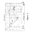
- Fig. 2 shows the performance of the first embodiment's all-tab structure in the frequency range of 290 MHz to 2.0 GHz.
- the present invention provides 60 dB of signal attenuation, while the conventional structure provides only 30 dB of attenuation.
- the first embodiment of the present invention is suitable for enclosure implementations having orthogonal panel orientations and some material overlap. Its superior EMC performance makes it an attractive and inexpensive alternative to more conventional approaches. In applications where a very level of attenuation is required, the present invention may be the only reasonable solution.
Landscapes
- Engineering & Computer Science (AREA)
- Microelectronics & Electronic Packaging (AREA)
- Shielding Devices Or Components To Electric Or Magnetic Fields (AREA)
- Casings For Electric Apparatus (AREA)
Applications Claiming Priority (2)
| Application Number | Priority Date | Filing Date | Title |
|---|---|---|---|
| US925983 | 1986-11-03 | ||
| US92598397A | 1997-09-09 | 1997-09-09 |
Publications (3)
| Publication Number | Publication Date |
|---|---|
| EP0902612A2 true EP0902612A2 (de) | 1999-03-17 |
| EP0902612A3 EP0902612A3 (de) | 1999-09-29 |
| EP0902612B1 EP0902612B1 (de) | 2003-04-02 |
Family
ID=25452539
Family Applications (1)
| Application Number | Title | Priority Date | Filing Date |
|---|---|---|---|
| EP19980306259 Expired - Lifetime EP0902612B1 (de) | 1997-09-09 | 1998-08-05 | Fügeanordnung für Gehäuse |
Country Status (3)
| Country | Link |
|---|---|
| EP (1) | EP0902612B1 (de) |
| JP (1) | JPH11145675A (de) |
| DE (1) | DE69812813T2 (de) |
Cited By (2)
| Publication number | Priority date | Publication date | Assignee | Title |
|---|---|---|---|---|
| EP1128715A3 (de) * | 2000-02-28 | 2003-09-03 | Mitsumi Electric Co., Ltd. | Abschirmgehäuse für ein elektronisches Gerät |
| US12108582B2 (en) | 2019-02-25 | 2024-10-01 | Mitsubishi Heavy Industries, Ltd. | Electronic device protection unit and electronic system |
Family Cites Families (4)
| Publication number | Priority date | Publication date | Assignee | Title |
|---|---|---|---|---|
| JPH0730277A (ja) * | 1993-07-12 | 1995-01-31 | Toshiba Corp | シールド装置 |
| JPH07221481A (ja) * | 1994-02-04 | 1995-08-18 | Matsushita Electric Ind Co Ltd | プリント配線基板のシールド装置 |
| DE59605897D1 (de) * | 1995-02-14 | 2000-10-26 | Knuerr Mechanik Ag | Rahmenkonstruktion für Gestelle und Gehäuse von Baugruppenträgern und Schränken zur Aufnahme von elektrischen und/oder elektronischen Bauteilen |
| JPH0927691A (ja) * | 1995-07-13 | 1997-01-28 | Fuji Electric Co Ltd | プリント基板へのシールドケース取付構造 |
-
1998
- 1998-08-05 EP EP19980306259 patent/EP0902612B1/de not_active Expired - Lifetime
- 1998-08-05 DE DE69812813T patent/DE69812813T2/de not_active Expired - Fee Related
- 1998-09-02 JP JP24796198A patent/JPH11145675A/ja active Pending
Cited By (2)
| Publication number | Priority date | Publication date | Assignee | Title |
|---|---|---|---|---|
| EP1128715A3 (de) * | 2000-02-28 | 2003-09-03 | Mitsumi Electric Co., Ltd. | Abschirmgehäuse für ein elektronisches Gerät |
| US12108582B2 (en) | 2019-02-25 | 2024-10-01 | Mitsubishi Heavy Industries, Ltd. | Electronic device protection unit and electronic system |
Also Published As
| Publication number | Publication date |
|---|---|
| JPH11145675A (ja) | 1999-05-28 |
| DE69812813D1 (de) | 2003-05-08 |
| EP0902612A3 (de) | 1999-09-29 |
| EP0902612B1 (de) | 2003-04-02 |
| DE69812813T2 (de) | 2004-03-04 |
Similar Documents
| Publication | Publication Date | Title |
|---|---|---|
| US5691504A (en) | Multilayer computer chassis having integral circuit board mounting and grounding structure | |
| US6297446B1 (en) | High performance EMC vent panel | |
| US5006667A (en) | Method and apparatus for shielding a printed circuit board | |
| US5045973A (en) | Procedure for manufacturing a radio telephone chassis and a chassis manufactured according to this procedure | |
| EP1951021B1 (de) | Abschirmvorrichtung für elektromagnetische Interferenz und Herstellungsverfahren dafür | |
| CA1319746C (en) | Rfi shielding gasket | |
| US6194653B1 (en) | Enclosure design having an integrated system of retention, electromagnetic interference containment and structural load distribution | |
| US5899755A (en) | Integrated circuit test socket with enhanced noise imminity | |
| US20030218873A1 (en) | Structure for fastening a component | |
| US6711032B2 (en) | Shield and method for shielding an electronic device | |
| EP1065759A2 (de) | Verbindungs- und Erdungsanordnung für einen abgeschirmten und einen Aufnahmeverbinder | |
| EP0351070B1 (de) | Doppelwandiges Ablenkelement zur Belüftung und elektromagnetischen Abschirmung | |
| WO2011090788A1 (en) | Rf interference suppressor | |
| EP0726700B1 (de) | Abschirmungsvorrichtung | |
| US7457134B2 (en) | Electromagnetic radiation containment system | |
| US7132609B2 (en) | Chassis spring finger tortuous path with improved manufacturability | |
| US5256086A (en) | Electrical connector shield and method of fabricating same | |
| EP0902612B1 (de) | Fügeanordnung für Gehäuse | |
| ZA200605484B (en) | Electronic apparatus and enclosure employing substantially co-planar portions with mating crenellations | |
| EP0139623A1 (de) | Kontaktvorrichtung als Schirm für elektronische Komponenten gegen elektromagnetische Strahlung | |
| US5827998A (en) | Electromagnetic shielding structure having radio wave-absorbing material | |
| US6582785B2 (en) | Shield case for electronic equipment | |
| US6608758B1 (en) | Chassis shielding system | |
| US5796594A (en) | Interlocking circuit card faceplate for reduced EMI emissions | |
| JP3019024B2 (ja) | Icカードソケット |
Legal Events
| Date | Code | Title | Description |
|---|---|---|---|
| PUAI | Public reference made under article 153(3) epc to a published international application that has entered the european phase |
Free format text: ORIGINAL CODE: 0009012 |
|
| AK | Designated contracting states |
Kind code of ref document: A2 Designated state(s): DE FR GB |
|
| AX | Request for extension of the european patent |
Free format text: AL;LT;LV;MK;RO;SI |
|
| PUAL | Search report despatched |
Free format text: ORIGINAL CODE: 0009013 |
|
| AK | Designated contracting states |
Kind code of ref document: A3 Designated state(s): AT BE CH CY DE DK ES FI FR GB GR IE IT LI LU MC NL PT SE |
|
| AX | Request for extension of the european patent |
Free format text: AL;LT;LV;MK;RO;SI |
|
| 17P | Request for examination filed |
Effective date: 20000124 |
|
| AKX | Designation fees paid |
Free format text: DE FR GB |
|
| RAP1 | Party data changed (applicant data changed or rights of an application transferred) |
Owner name: HEWLETT-PACKARD COMPANY, A DELAWARE CORPORATION |
|
| GRAG | Despatch of communication of intention to grant |
Free format text: ORIGINAL CODE: EPIDOS AGRA |
|
| 17Q | First examination report despatched |
Effective date: 20020531 |
|
| GRAG | Despatch of communication of intention to grant |
Free format text: ORIGINAL CODE: EPIDOS AGRA |
|
| GRAH | Despatch of communication of intention to grant a patent |
Free format text: ORIGINAL CODE: EPIDOS IGRA |
|
| GRAH | Despatch of communication of intention to grant a patent |
Free format text: ORIGINAL CODE: EPIDOS IGRA |
|
| GRAA | (expected) grant |
Free format text: ORIGINAL CODE: 0009210 |
|
| RIN1 | Information on inventor provided before grant (corrected) |
Inventor name: WORTMAN, MICHAEL Inventor name: CHERNISKI, ANDREW M. |
|
| AK | Designated contracting states |
Designated state(s): DE FR GB |
|
| REG | Reference to a national code |
Ref country code: GB Ref legal event code: FG4D |
|
| REF | Corresponds to: |
Ref document number: 69812813 Country of ref document: DE Date of ref document: 20030508 Kind code of ref document: P |
|
| ET | Fr: translation filed | ||
| PLBE | No opposition filed within time limit |
Free format text: ORIGINAL CODE: 0009261 |
|
| STAA | Information on the status of an ep patent application or granted ep patent |
Free format text: STATUS: NO OPPOSITION FILED WITHIN TIME LIMIT |
|
| 26N | No opposition filed |
Effective date: 20040105 |
|
| PGFP | Annual fee paid to national office [announced via postgrant information from national office to epo] |
Ref country code: GB Payment date: 20070830 Year of fee payment: 10 |
|
| PGFP | Annual fee paid to national office [announced via postgrant information from national office to epo] |
Ref country code: DE Payment date: 20071001 Year of fee payment: 10 |
|
| PGFP | Annual fee paid to national office [announced via postgrant information from national office to epo] |
Ref country code: FR Payment date: 20070817 Year of fee payment: 10 |
|
| GBPC | Gb: european patent ceased through non-payment of renewal fee |
Effective date: 20080805 |
|
| REG | Reference to a national code |
Ref country code: FR Ref legal event code: ST Effective date: 20090430 |
|
| PG25 | Lapsed in a contracting state [announced via postgrant information from national office to epo] |
Ref country code: FR Free format text: LAPSE BECAUSE OF NON-PAYMENT OF DUE FEES Effective date: 20080901 Ref country code: DE Free format text: LAPSE BECAUSE OF NON-PAYMENT OF DUE FEES Effective date: 20090303 |
|
| PG25 | Lapsed in a contracting state [announced via postgrant information from national office to epo] |
Ref country code: GB Free format text: LAPSE BECAUSE OF NON-PAYMENT OF DUE FEES Effective date: 20080805 |