EP0902573A2 - Leitungsempfänger mit galavanischer Trennung - Google Patents
Leitungsempfänger mit galavanischer Trennung Download PDFInfo
- Publication number
- EP0902573A2 EP0902573A2 EP98116121A EP98116121A EP0902573A2 EP 0902573 A2 EP0902573 A2 EP 0902573A2 EP 98116121 A EP98116121 A EP 98116121A EP 98116121 A EP98116121 A EP 98116121A EP 0902573 A2 EP0902573 A2 EP 0902573A2
- Authority
- EP
- European Patent Office
- Prior art keywords
- current
- output
- current mirror
- arrangement
- signal
- Prior art date
- Legal status (The legal status is an assumption and is not a legal conclusion. Google has not performed a legal analysis and makes no representation as to the accuracy of the status listed.)
- Withdrawn
Links
Images

Classifications
-
- H—ELECTRICITY
- H04—ELECTRIC COMMUNICATION TECHNIQUE
- H04L—TRANSMISSION OF DIGITAL INFORMATION, e.g. TELEGRAPHIC COMMUNICATION
- H04L25/00—Baseband systems
- H04L25/02—Details ; arrangements for supplying electrical power along data transmission lines
- H04L25/0264—Arrangements for coupling to transmission lines
- H04L25/0266—Arrangements for providing Galvanic isolation, e.g. by means of magnetic or capacitive coupling
Definitions
- the invention relates to a circuit for recovering a digital signal from a by means of galvanic isolation input signal with two input connections for the input signal and an output terminal for the recovered digital signal.
- the use of the coupling elements causes a change of the waveform, so that when transmitting a Signals from system A to system B in system B a facility is to be provided with which the system A emitted waveform can be recovered. This is required especially with digital signals because the digital signal processing equipment in the receiving System B only reliable with defined signal structures work.
- the technical problem underlying the invention exists therefore in specifying a circuit with which a digital Signal sent to a receiver system using electrical isolation is supplied, recovered from the received signal can be.
- a preferred signal regeneration circuit accordingly has a current direction sensor on the between the input terminals prevailing current direction detected and a Output signal according to the current direction.
- the current direction sensor detects the direction of the Current that flows between the two input connections.
- the current direction sensor preferably has a voltage clamping arrangement and a current mirror arrangement.
- the voltage clamp arrangement sets the voltage between the input terminals to a predetermined maximum value.
- the Current mirror arrangement detects the between the input terminals flowing current and leads the detected current value an output driver arrangement to which the output signal is tapped. It is particularly preferred that the voltage clamp arrangement a first and a second series connection from at least two each switched in the same direction Has diodes.
- the diodes are the first Series connection in the opposite direction to the diodes the second series connection, and the series connections are connected to each other at a middle node.
- the signal regeneration circuit has the current mirror arrangement of the current direction sensor a first and a second Current mirror on.
- the first current mirror forms the Current flow through the voltage clamp assembly in a first Current flow direction
- the second current mirror forms the Current flow through the voltage clamp assembly in a second Current flow direction.
- the current mirror arrangement a third and a fourth current mirror.
- the third current mirror is connected to the output current path of the first current mirror and the fourth current mirror is with the output current path connected to the second current mirror.
- Very particularly preferred is a version in which the output current path of the third current mirror and the output current path of the fourth Current mirrors are connected together and the output driver arrangement form. At the junction of the output current paths of the third and fourth current mirror then the output signal can be tapped.
- a reference potential can be supplied.
- the reference potential is compared to the ground potential of the current direction sensor, and thus the signal receiving system.
- the circuit structures of the current mirror arrangement can then be compared to the ground potential of the receiving Systems can be designed.
- This reference potential is preferably in the area of the threshold potential of CMOS transistors, when such transistors are used in the circuit should be. It is preferred to switch the circuit off to build bipolar transistors and CMOS transistors.
- the input signal is preferably capacitive Coupling fed.
- the current direction sensor a buffer, preferably in the form a flip-flop, with which the last ruling Current direction state is cached.
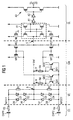
- Figure 1 is essentially divided into four circuit blocks.
- a circuit block CC relates to capacitive coupling two signal lines.
- Circuit blocks VC, CM and OL together form a current direction sensor according to a preferred Embodiment of the invention.
- the current direction sensor according to Figure 1 has a voltage clamp arrangement VC, a current mirror arrangement CM and a buffer arrangement OL on.
- the capacitive coupling CC is the Current direction sensor a typically differential input signal supplied, which is evaluated by the current direction sensor and at its output terminal OUTPUT as recovered Input signal is output.
- the capacitive coupling arrangement points to this in each of the signal lines a coupling capacitor CHP1 and CHP2 and each a resistor R3 or R4 connected in series.
- the free connections of the resistors R3 and R4 are with the Input signal connections INPUT1 or INPUT2 of the voltage terminal arrangement VC of the current direction sensor connected.
- the voltage terminal arrangement has two rows of diodes D1, D2, D3, D4 and D5, D6, D7, D8 connected in anti-parallel which are connected at their free ends to the input signal connections INPUT1 and INPUT2.
- a series connection of resistors R1 and R2 is connected in parallel with the diode series connections, the free ends of which are also connected to the signal input connections INPUT1 and INPUT2.
- the two diode series connections and the resistance series connection are connected to one another at a center node B.
- the center node B lies at a reference potential Vref which is fixed in relation to the ground potential of the receiving system.
- the signal input connections INPUT1 and INPUT2 are thus two diode forward voltages V D above and below the reference voltage Vref with respect to the ground potential of the receiving system to which the current direction sensor belongs.
- the diodes D1 to D8 are preferably designed as bipolar transistors, the collector and base of which are short-circuited and thus simulate the function of a diode in the integrated circuit in a simple manner.
- the input current paths of a first and a second current mirror are connected between the center node B and the node of the input signal connection INPUT2.
- the input current path of the first current mirror has a resistor RX and a bipolar transistor QX1 of the NPN type short-circuited to a diode.
- the input current path of the first current mirror is thus connected in the same forward direction as the diode series circuit D1 to D4.
- the input current path of the second current mirror has a resistor RY and a bipolar transistor QY1 of the pnp type short-circuited as a diode.
- the input current path of the second current mirror has the same forward direction as the diode series circuit D5 to D8.
- the maximum current IX through the input current path of the first current mirror and the maximum current through the input current path of the second current mirror are equal in amount. However, the current direction is opposite according to the diode switching direction. The amount is:
- (2V D -V BE ) / RX, where V D is the forward voltage of a diode of the diode series circuits D1 to D8 and where V BE is the base-emitter voltage of the transistor QX1 and QY1.
- the collector-emitter path lies in the output current path of the first current mirror an npn transistor QX2, and in the output current path the collector current emitter lies on the second current mirror a PNP transistor QY2.
- the basic connections and the emitter terminals of transistors QX1 and QX2 and the transistors QY1 and QY2 are connected to one another, to form a current mirror.
- the output rung of the first current mirror is one with the input current path third current mirror connected and the output current path of the second current mirror is one with the input current path fourth current mirror connected.
- In the input current path of the The third current mirror is the load path of a p-channel MOS transistor MX1.
- the free end of the load section of the Transistor MX1 is connected to the supply voltage connection of the receiving system connected.
- the gate connection of the transistor MX1 with the connection node of the Transistors QX2 and MX1 connected.
- the output current path of the second current mirror with the Input current path of a fourth current mirror connected.
- the input current path of the fourth current mirror is the Load path of an n-channel MOS transistor MY1, the free one End of the load path with the ground potential of the receiving one System is connected.
- the gate of transistor MY1 is with the connection node of transistors QY2 and MY1 connected.
- the output current path of the third current mirror is from a p-channel MOS transistor MX2, and the output current path the fourth current mirror is from the load path of an n-channel MOS transistor MY2 is formed.
- the free end the load path of the transistor MX2 is connected to the supply voltage connection of the receiving system and that free end of the load path of transistor MY2 is connected to the Ground connection of the receiving system connected.
- the gate connections their transistors MX1 and MX2 and Transistors MY1 and MY2 are connected to one another To form current mirror.
- the load paths of the transistors MX2 and MY2 of the third and fourth current mirrors connected to each other at a node S. At node S can a logical signal can be tapped that the currently prevailing current direction between the input connections INPUT1 and INPUT2 displays.
- the current mirror arrangement CM is the output buffer arrangement OL downstream, with which the output signal is stabilized at the node S of the current mirror arrangement CM.
- the output latch circuit OL has one of CMOS inverters existing flip-flop FF, whose input connection with the output node S of the current mirror arrangement CM connected is.
- One of the inverters of the flip-flop FF points in addition, load transistors ML1 and ML2, which also are configured in complementary MOS technology.
- the inverter A3 is configured and dimensioned as a CMOS output driver.
- the output signal is at the output terminal of the inverter A3 OUTPUT of the signal regeneration circuit of the invention.
- the voltage clamp arrangement with the antiparallel connected diode series circuits D1 to D4 or D5 to D8 clamps the voltage between the signal input connections INPUT1 and INPUT2 to a value which is four times the amount of a diode forward voltage V D. Relative to the center node B, the voltage at the signal input connection INPUT2 moves the voltage between Vref + 2 V D and Vref - 2 V D in relation to the ground potential of the receiving system. It should be mentioned that with a rectangular, differential input signal applied to the capacitors CHP1 and CHP2, the capacitors CHP1 and CHP2 discharge exponentially via the resistors R1 and R2 after each voltage level change in the input signal.
- the current direction of the discharge current determines the logical state of the input signal.
- a first current direction is detected in the input current path of the first current mirror
- the second current direction is detected in the input current path of the second current mirror.
- the input current paths of the first and second current mirrors are connected between the central node B and the node of the input connection INPUT2 according to FIG. 1, the circuit function can also be implemented with only a slightly different configuration if the input current path of the first or second current mirror or of the first and second current mirror is connected between the middle node B and the node of the input connection INPUT1.
- the current IX in the input current path of the first current mirror is mapped into its output current path and simultaneously fed to the input current path of the third current mirror.
- the current IY in the input current path of the second current mirror mapped in its output current path and supplied to the input current path of the fourth current mirror. Because at any given time either only the first or only the second current mirror is active the output current paths of the third and fourth current mirrors can be connected to each other in order to connect the connection node S To tap the output signal.
- the reference voltage Vref is based on the ground potential of the receiving system.
- a current IY as calculated above thus flows through the input current path of the second current mirror. This current IY is mapped onto the output current path of the second current mirror, multiplied by the fourth current mirror and applied to the flip-flop FF via the node S in order to switch this state.
- the flip-flop thus switches according to the current direction currently prevailing between the input connections INPUT1 and INPUT2.
- the switching currents of the flip-flop FF can be set with the load transistors ML1 and ML2.
- FIG. 2 shows a circuit for generating the reference potential Vref.
- a current I B is supplied to a node A, the value of which is very low.
- This current flows via diode-connected npn transistors QB1 and QB2 and the load path of an n-channel MOS transistor to the ground connection of the receiving system.
- this current is mapped into an output current path via the transistors MB1 and MB2 connected to form a current mirror.
- the output current path consists of the load path of the transistor MB2, the collector-emitter path of an npn transistor QB7, which is also connected to the current mirror by the transistor QB2, and the load path of a p-channel MOS transistor MB5.
- the current in the output current path of the current mirror arrangement is mapped onto the load path of a p-channel MOS transistor MB6 via the transistor MB5.
- This activates a pnp transistor QB4 and drives a further current mirror arrangement consisting of the n-channel MOS transistors MB3 and MB4.
- the load path of the transistor MB4 and the collector-emitter path of an NPN transistor QB3, which is also activated as a result, is located in the output current path of this current mirror.
- the base of an output transistor QB5 of the npn type is connected to a connection node Y of the transistor MB6 and the transistor QB4.
- the base of an output transistor QB6 of the PNP type is connected to a connection node X between the emitter of transistor QB3 and the load path of transistor MB4.
- the emitters of the output transistors QB5 and QB6 are connected to one another and are at the desired voltage Vref.
- the voltage Vref is at the same level as the potential at node A. This is because the rabbits of the Transistors QB3 and QB4 also connected to node A. and transistors QB3 and QB4 from the current mirror arrays from the transistors MB3 and MB4 or MB5 and MB6 kept activated.
- the node Y is around the Voltage drop across the base-emitter diode of the transistor QB4 above the potential of node A. About the voltage drop reaches the base-emitter diode of transistor QB5 then back to the potential of node A.
- the circuit of Figure 2 belongs to the receiving system and is therefore related to its ground potential. This is true also to the supply voltage connections illustrated in FIG. 2 at the free ends of the load routes of the transistors MB5, MB6, QB3 and QB5. Between the knot A and the ground potential is also a capacitor C1 switched, the high-frequency noise from a surrounding Supply voltage sources or clock system sources filtered out.
- the voltage at node A and thus the output voltage Vref is twice the base-emitter voltage above the threshold voltage of a MOS transistor related to the ground potential of the receiving system.
Landscapes
- Engineering & Computer Science (AREA)
- Power Engineering (AREA)
- Computer Networks & Wireless Communication (AREA)
- Signal Processing (AREA)
- Logic Circuits (AREA)
- Amplifiers (AREA)
- Circuits Of Receivers In General (AREA)
Abstract
Description
- Figur 1
- ein bevorzugtes Ausführungsbeispiel der Signalregenerierungsschaltung gemäß der Erfindung und
- Figur 2
- eine Schaltung zur Erzeugung eines Bezugspotentials.
Claims (11)
- Signalregenerierungsschaltung zum Wiedergewinnen eines digitalen Signals aus einem mittels galvanischer Trennung (CHP1, CHP2) zugeführten Eingangssignal mit zwei Eingangsanschlüssen (INPUT1, INPUT2) für das Eingangssignal und einem Ausgangsanschluß (OUTPUT) für das wiedergewonnene digitale Signal,
gekennzeichnet durch
einen Stromrichtungssensor (VC, CM, OL), der die zwischen den Eingangsanschlüssen (INPUT1, INPUT2) herrschende Stromrichtung erfaßt und der ein Signal (OUTPUT) entsprechend der herrschenden Stromrichtung abgibt. - Schaltung nach Patentanspruch 1,
dadurch gekennzeichnet, daß
der Stromrichtungssensor eine Spannungsklemmanordnung (VC) zum Festlegen der Spannung zwischen den Eingangsanschlüssen (INPUT1, INPUT2) und eine Stromspiegelanordnung (CM), die eine Ausgangstreiberanordnung (MX2, MY2) umfaßt, aufweist, wobei das Ausgangssignal (OUTPUT) an der Ausgangstreiberanordnung (MX2, MY2) abgreifbar ist. - Schaltung nach Patentanspruch 2,
dadurch gekennzeichnet, daß
die Spannungsklemmanordnung (VC) eine erste (D1, D2, D3, D4) und eine zweite (D5, D6, D7, D8) Reihenschaltung aus jeweils mindestens zwei in gleicher Richtung geschalteter Dioden aufweist, wobei die Dioden der ersten Reihenschaltung (D1, D2, D3, D4) in entgegengesetzter Richtung zu den Dioden der zweiten Reihenschaltung (D5, D6, D7, D8) geschaltet sind und die Reihenschaltungen an einem Mittelknoten miteinander verbunden sind. - Schaltung nach einem der Patentansprüche 2 oder 3,
dadurch gekennzeichnet, daß
die Stromspiegelanordnung (CM) einen ersten (QX1, QX2, RX) und einen zweiten (QY1, QY2, RY) Stromspiegel aufweist, wobei der erste Stromspiegel (QX1, QX2, RX) den Stromfluß (IX) durch die Spannungsklemmanordnung (VC) in einer ersten Stromflußrichtung abbildet und der zweite Stromspiegel (QY1, QY2, RY) den Stromfluß (IY) durch die Spannungsklemmanordnung (VC) in einer zweiten Stromflußrichtung abbildet. - Schaltung nach Patentanspruch 4,
dadurch gekennzeichnet, daß
die Stromspiegelanordnung (CM) einen dritten (MX1, MX2) und einen vierten (MY1, MY2) Stromspiegel aufweist, wobei der dritte Stromspiegel (MX1, MX2) mit dem Ausgangsstrompfad des ersten Stromspiegels (QX1, QX2, RX) verbunden ist und der vierte Stromspiegel (MY1, MY2) mit dem Ausgangsstrompfad des zweiten Stromspiegels (QY1, QY2, RY) verbunden ist. - Schaltung nach Patentanspruch 5,
dadurch gekennzeichnet, daß
der Ausgangsstrompfad des dritten Stromspiegels (MX1, MX2) und der Ausgangsstrompfad des vierten Stromspiegels (MY1, MY2) miteinander verbunden sind und die Ausgangstreiberanordnung (MX2, MY2) bilden, wobei am Verbindungsknoten (S) der Ausgangsstrompfade des dritten und vierten Stromspiegels das Ausgangssignal abgegriffen werden kann. - Schaltung nach einem der Patentansprüche 2 bis 6,
dadurch gekennzeichnet, daß
an dem Mittelknoten der Spannungsklemmanordnung (VC) ein Hezugspotential (Vref) zuführbar ist. - Schaltung nach einem der Patentansprüche 7,
dadurch gekennzeichnet, daß
das Bezugspotential (Vref) im Bereich des Schwellenpotentials (VT) der in einer integrierten Schaltung verwendeten CMOS-Transistoren liegt. - Schaltung nach einem der vorhergehenden Patentansprüche,
dadurch gekennzeichnet, daß
die Schaltung aus Bipolaren Transistoren und CMOS Transistoren aufgebaut ist. - Schaltung nach einem der vorhergehenden Patentansprüche,
dadurch gekennzeichnet, daß
das Eingangssignal mittels kapazitiver Kopplung (CHP1, CHP2) zugeführt ist. - Schaltung nach einem der vorhergehenden Patentansprüche,
dadurch gekennzeichnet, daß
der Stromrichtungssensor (VC, CM, OL) einen Zwischenspeicher (OL) aufweist, mit dem der zuletzt herrschende Stromrichtungszustand zwischengespeichert wird.
Applications Claiming Priority (2)
| Application Number | Priority Date | Filing Date | Title |
|---|---|---|---|
| DE19739960A DE19739960C2 (de) | 1997-09-11 | 1997-09-11 | Signalregenerierungsschaltung |
| DE19739960 | 1997-09-11 |
Publications (2)
| Publication Number | Publication Date |
|---|---|
| EP0902573A2 true EP0902573A2 (de) | 1999-03-17 |
| EP0902573A3 EP0902573A3 (de) | 2001-10-04 |
Family
ID=7842023
Family Applications (1)
| Application Number | Title | Priority Date | Filing Date |
|---|---|---|---|
| EP98116121A Withdrawn EP0902573A3 (de) | 1997-09-11 | 1998-08-26 | Leitungsempfänger mit galavanischer Trennung |
Country Status (3)
| Country | Link |
|---|---|
| US (1) | US6225832B1 (de) |
| EP (1) | EP0902573A3 (de) |
| DE (1) | DE19739960C2 (de) |
Family Cites Families (17)
| Publication number | Priority date | Publication date | Assignee | Title |
|---|---|---|---|---|
| US3550007A (en) * | 1967-05-29 | 1970-12-22 | Scm Corp | Variable threshold signal detection and isolation circuit |
| US3754193A (en) * | 1971-04-19 | 1973-08-21 | C Reinhard | Input bias and signal conditioning circuit for differential amplifiers |
| US3883812A (en) * | 1971-12-20 | 1975-05-13 | Nasa | Diode-quad bridge circuit means |
| US3838224A (en) * | 1973-05-17 | 1974-09-24 | L Richards | Electronic telephone trunk circuit |
| US4070600A (en) * | 1976-12-23 | 1978-01-24 | General Electric Company | High voltage driver circuit |
| US4161693A (en) * | 1977-03-09 | 1979-07-17 | Airpax Electronics, Inc. | Clamped input common mode rejection amplifier |
| GB1529043A (en) * | 1977-03-17 | 1978-10-18 | Standard Telephones Cables Ltd | Direct current direction detecting circuit |
| US4401901A (en) * | 1981-06-01 | 1983-08-30 | Advanced Micro Devices, Inc. | Comparator |
| US4728815A (en) * | 1986-10-16 | 1988-03-01 | Motorola, Inc. | Data shaping circuit |
| KR910008101B1 (ko) * | 1988-12-30 | 1991-10-07 | 삼성전자 주식회사 | 반도체 메모리 소자의 피드백형 데이타 출력 회로 |
| IT1236879B (it) * | 1989-11-22 | 1993-04-26 | Sgs Thomson Microelectronics | Circuito elettronico comparatore |
| US5287070A (en) * | 1992-09-02 | 1994-02-15 | Ncr Corporation | Balanced voltage comparator |
| GB2293739B (en) * | 1994-09-29 | 1999-02-03 | Sony Uk Ltd | Balanced output driver |
| JP2885120B2 (ja) * | 1995-01-27 | 1999-04-19 | 日本電気株式会社 | 演算増幅器 |
| US5621340A (en) * | 1995-08-02 | 1997-04-15 | Rambus Inc. | Differential comparator for amplifying small swing signals to a full swing output |
| EP0798885A2 (de) | 1996-03-26 | 1997-10-01 | Siemens Aktiengesellschaft | Schaltungsanordnung zur Kopplung eines analogen Übertragungswegs mit einem digitalen Übertragungsweg |
| JP3881079B2 (ja) * | 1997-03-14 | 2007-02-14 | 株式会社アドバンテスト | 半導体集積回路素子 |
-
1997
- 1997-09-11 DE DE19739960A patent/DE19739960C2/de not_active Expired - Fee Related
-
1998
- 1998-08-26 EP EP98116121A patent/EP0902573A3/de not_active Withdrawn
- 1998-09-11 US US09/151,964 patent/US6225832B1/en not_active Expired - Lifetime
Also Published As
| Publication number | Publication date |
|---|---|
| EP0902573A3 (de) | 2001-10-04 |
| DE19739960C2 (de) | 2000-11-30 |
| US6225832B1 (en) | 2001-05-01 |
| DE19739960A1 (de) | 1999-04-01 |
Similar Documents
| Publication | Publication Date | Title |
|---|---|---|
| EP0288016B1 (de) | Komparator mit erweitertem Eingangsgleichtaktspannungsbereich | |
| EP0094044A2 (de) | Schaltungsanordnung zur Pegelumsetzung | |
| DE3338124C2 (de) | ||
| EP0093996B1 (de) | Schaltungsanordnung zur Pegelumsetzung | |
| EP0725996B1 (de) | Steuerschaltung | |
| DE3937501A1 (de) | Verfahren und vorrichtung zur erzeugung einer vorspannung | |
| DE69528845T2 (de) | N-bit umsetzer mit n-1-grössenverstärkern und n-vergleichern | |
| DE2836445C2 (de) | Schaltungsanordnung zur Fehlererkennung in Digitalsignalen | |
| DE2416534B2 (de) | Transistorschaltung zum umkehren der stromrichtung in einem verbraucher | |
| DE2717059A1 (de) | Automatische verstaerkungs-steuerschaltung | |
| DE3525522C2 (de) | ||
| EP0021085A2 (de) | Monolithisch integrierbarer Transistorverstärker | |
| EP1099308B1 (de) | Treiberschaltung | |
| DE3136910A1 (de) | Signalunterbrechungsschaltung | |
| EP0421016A1 (de) | ECL-TTL-Signalpegelwandler | |
| DE19739960C2 (de) | Signalregenerierungsschaltung | |
| DE3832378C1 (de) | ||
| DE69118249T2 (de) | Verriegelschaltung | |
| DE3110355A1 (de) | "vorspannungsgenerator" | |
| DE3017566C2 (de) | Verstärker, insbesondere für eine Teilnehmerschaltung | |
| EP0436823A1 (de) | Signalpegelwandler | |
| DE3718001C2 (de) | ||
| DE2831278A1 (de) | Schaltungsanordnung zur begrenzung der ausgangsspannung eines verstaerkers | |
| EP0904576A1 (de) | Stromversorgungsschaltung | |
| EP0676846B1 (de) | Schalter mit einem als Bipolartransistor ausgebildeten ersten Schaltelement |
Legal Events
| Date | Code | Title | Description |
|---|---|---|---|
| PUAI | Public reference made under article 153(3) epc to a published international application that has entered the european phase |
Free format text: ORIGINAL CODE: 0009012 |
|
| AK | Designated contracting states |
Kind code of ref document: A2 Designated state(s): AT BE CH CY DE DK ES FI FR GB GR IE IT LI LU MC NL PT SE |
|
| AX | Request for extension of the european patent |
Free format text: AL;LT;LV;MK;RO;SI |
|
| PUAL | Search report despatched |
Free format text: ORIGINAL CODE: 0009013 |
|
| AK | Designated contracting states |
Kind code of ref document: A3 Designated state(s): AT BE CH CY DE DK ES FI FR GB GR IE IT LI LU MC NL PT SE |
|
| AX | Request for extension of the european patent |
Free format text: AL;LT;LV;MK;RO;SI |
|
| RAP1 | Party data changed (applicant data changed or rights of an application transferred) |
Owner name: INFINEON TECHNOLOGIES AG |
|
| AKX | Designation fees paid | ||
| REG | Reference to a national code |
Ref country code: DE Ref legal event code: 8566 |
|
| STAA | Information on the status of an ep patent application or granted ep patent |
Free format text: STATUS: THE APPLICATION IS DEEMED TO BE WITHDRAWN |
|
| 18D | Application deemed to be withdrawn |
Effective date: 20020405 |