EP0902482A1 - SOI-MOSFET and fabrication process thereof - Google Patents
SOI-MOSFET and fabrication process thereof Download PDFInfo
- Publication number
- EP0902482A1 EP0902482A1 EP98305138A EP98305138A EP0902482A1 EP 0902482 A1 EP0902482 A1 EP 0902482A1 EP 98305138 A EP98305138 A EP 98305138A EP 98305138 A EP98305138 A EP 98305138A EP 0902482 A1 EP0902482 A1 EP 0902482A1
- Authority
- EP
- European Patent Office
- Prior art keywords
- soi
- top semiconductor
- mosfet
- conductivity type
- gate electrode
- Prior art date
- Legal status (The legal status is an assumption and is not a legal conclusion. Google has not performed a legal analysis and makes no representation as to the accuracy of the status listed.)
- Granted
Links
- 238000000034 method Methods 0.000 title claims description 32
- 230000008569 process Effects 0.000 title claims description 23
- 238000004519 manufacturing process Methods 0.000 title description 10
- 239000004065 semiconductor Substances 0.000 claims abstract description 63
- 239000000758 substrate Substances 0.000 claims abstract description 50
- 150000002500 ions Chemical class 0.000 claims abstract description 38
- 238000002513 implantation Methods 0.000 claims abstract description 33
- 239000012535 impurity Substances 0.000 claims description 41
- 125000006850 spacer group Chemical group 0.000 claims description 11
- 238000007667 floating Methods 0.000 claims description 6
- 230000000694 effects Effects 0.000 abstract description 13
- 108091006146 Channels Proteins 0.000 description 42
- 239000010408 film Substances 0.000 description 32
- XUIMIQQOPSSXEZ-UHFFFAOYSA-N Silicon Chemical compound [Si] XUIMIQQOPSSXEZ-UHFFFAOYSA-N 0.000 description 24
- 229910052710 silicon Inorganic materials 0.000 description 24
- 239000010703 silicon Substances 0.000 description 24
- VYPSYNLAJGMNEJ-UHFFFAOYSA-N Silicium dioxide Chemical compound O=[Si]=O VYPSYNLAJGMNEJ-UHFFFAOYSA-N 0.000 description 8
- 230000003071 parasitic effect Effects 0.000 description 4
- 238000000926 separation method Methods 0.000 description 4
- 238000000137 annealing Methods 0.000 description 3
- QVGXLLKOCUKJST-UHFFFAOYSA-N atomic oxygen Chemical compound [O] QVGXLLKOCUKJST-UHFFFAOYSA-N 0.000 description 3
- 229910052681 coesite Inorganic materials 0.000 description 3
- 229910052906 cristobalite Inorganic materials 0.000 description 3
- 238000005530 etching Methods 0.000 description 3
- 238000001465 metallisation Methods 0.000 description 3
- 239000001301 oxygen Substances 0.000 description 3
- 229910052760 oxygen Inorganic materials 0.000 description 3
- 229910052594 sapphire Inorganic materials 0.000 description 3
- 239000010980 sapphire Substances 0.000 description 3
- 229910021332 silicide Inorganic materials 0.000 description 3
- 239000000377 silicon dioxide Substances 0.000 description 3
- 229910052682 stishovite Inorganic materials 0.000 description 3
- 229910052905 tridymite Inorganic materials 0.000 description 3
- 102000004129 N-Type Calcium Channels Human genes 0.000 description 2
- 108090000699 N-Type Calcium Channels Proteins 0.000 description 2
- 230000015572 biosynthetic process Effects 0.000 description 2
- 239000004020 conductor Substances 0.000 description 2
- 238000009826 distribution Methods 0.000 description 2
- 238000005421 electrostatic potential Methods 0.000 description 2
- 238000005468 ion implantation Methods 0.000 description 2
- 239000002184 metal Substances 0.000 description 2
- 229910052751 metal Inorganic materials 0.000 description 2
- 238000012986 modification Methods 0.000 description 2
- 230000004048 modification Effects 0.000 description 2
- 238000000206 photolithography Methods 0.000 description 2
- 229910021420 polycrystalline silicon Inorganic materials 0.000 description 2
- FVBUAEGBCNSCDD-UHFFFAOYSA-N silicide(4-) Chemical compound [Si-4] FVBUAEGBCNSCDD-UHFFFAOYSA-N 0.000 description 2
- 229910001218 Gallium arsenide Inorganic materials 0.000 description 1
- 229910000530 Gallium indium arsenide Inorganic materials 0.000 description 1
- BLRPTPMANUNPDV-UHFFFAOYSA-N Silane Chemical compound [SiH4] BLRPTPMANUNPDV-UHFFFAOYSA-N 0.000 description 1
- 239000003990 capacitor Substances 0.000 description 1
- 230000015556 catabolic process Effects 0.000 description 1
- 238000005229 chemical vapour deposition Methods 0.000 description 1
- 150000001875 compounds Chemical class 0.000 description 1
- 238000010276 construction Methods 0.000 description 1
- 238000007796 conventional method Methods 0.000 description 1
- 230000008878 coupling Effects 0.000 description 1
- 238000010168 coupling process Methods 0.000 description 1
- 238000005859 coupling reaction Methods 0.000 description 1
- 230000000593 degrading effect Effects 0.000 description 1
- 238000000151 deposition Methods 0.000 description 1
- 238000009792 diffusion process Methods 0.000 description 1
- 239000007772 electrode material Substances 0.000 description 1
- 230000005669 field effect Effects 0.000 description 1
- 239000007789 gas Substances 0.000 description 1
- 229910052732 germanium Inorganic materials 0.000 description 1
- GNPVGFCGXDBREM-UHFFFAOYSA-N germanium atom Chemical compound [Ge] GNPVGFCGXDBREM-UHFFFAOYSA-N 0.000 description 1
- 239000011521 glass Substances 0.000 description 1
- 239000002784 hot electron Substances 0.000 description 1
- 239000012212 insulator Substances 0.000 description 1
- 230000010354 integration Effects 0.000 description 1
- 238000002955 isolation Methods 0.000 description 1
- 229910044991 metal oxide Inorganic materials 0.000 description 1
- 150000004706 metal oxides Chemical class 0.000 description 1
- 229910052750 molybdenum Inorganic materials 0.000 description 1
- 230000007935 neutral effect Effects 0.000 description 1
- 230000003647 oxidation Effects 0.000 description 1
- 238000007254 oxidation reaction Methods 0.000 description 1
- 238000000059 patterning Methods 0.000 description 1
- 230000000149 penetrating effect Effects 0.000 description 1
- 239000004033 plastic Substances 0.000 description 1
- 229920005591 polysilicon Polymers 0.000 description 1
- 238000004886 process control Methods 0.000 description 1
- 239000010453 quartz Substances 0.000 description 1
- 238000005215 recombination Methods 0.000 description 1
- 230000006798 recombination Effects 0.000 description 1
- 230000009467 reduction Effects 0.000 description 1
- 239000003870 refractory metal Substances 0.000 description 1
- 229910000077 silane Inorganic materials 0.000 description 1
- 229910052814 silicon oxide Inorganic materials 0.000 description 1
- 229910052715 tantalum Inorganic materials 0.000 description 1
- 239000010409 thin film Substances 0.000 description 1
- 229910052719 titanium Inorganic materials 0.000 description 1
- 229910052721 tungsten Inorganic materials 0.000 description 1
Images

Classifications
-
- H—ELECTRICITY
- H10—SEMICONDUCTOR DEVICES; ELECTRIC SOLID-STATE DEVICES NOT OTHERWISE PROVIDED FOR
- H10D—INORGANIC ELECTRIC SEMICONDUCTOR DEVICES
- H10D30/00—Field-effect transistors [FET]
- H10D30/01—Manufacture or treatment
- H10D30/021—Manufacture or treatment of FETs having insulated gates [IGFET]
- H10D30/031—Manufacture or treatment of FETs having insulated gates [IGFET] of thin-film transistors [TFT]
- H10D30/0321—Manufacture or treatment of FETs having insulated gates [IGFET] of thin-film transistors [TFT] comprising silicon, e.g. amorphous silicon or polysilicon
- H10D30/0323—Manufacture or treatment of FETs having insulated gates [IGFET] of thin-film transistors [TFT] comprising silicon, e.g. amorphous silicon or polysilicon comprising monocrystalline silicon
-
- H—ELECTRICITY
- H10—SEMICONDUCTOR DEVICES; ELECTRIC SOLID-STATE DEVICES NOT OTHERWISE PROVIDED FOR
- H10D—INORGANIC ELECTRIC SEMICONDUCTOR DEVICES
- H10D30/00—Field-effect transistors [FET]
- H10D30/60—Insulated-gate field-effect transistors [IGFET]
- H10D30/67—Thin-film transistors [TFT]
- H10D30/6704—Thin-film transistors [TFT] having supplementary regions or layers in the thin films or in the insulated bulk substrates for controlling properties of the device
- H10D30/6708—Thin-film transistors [TFT] having supplementary regions or layers in the thin films or in the insulated bulk substrates for controlling properties of the device for preventing the kink effect or the snapback effect, e.g. discharging the minority carriers of the channel region for preventing bipolar effect
-
- H—ELECTRICITY
- H01—ELECTRIC ELEMENTS
- H01L—SEMICONDUCTOR DEVICES NOT COVERED BY CLASS H10
- H01L21/00—Processes or apparatus adapted for the manufacture or treatment of semiconductor or solid state devices or of parts thereof
- H01L21/02—Manufacture or treatment of semiconductor devices or of parts thereof
- H01L21/04—Manufacture or treatment of semiconductor devices or of parts thereof the devices having potential barriers, e.g. a PN junction, depletion layer or carrier concentration layer
- H01L21/18—Manufacture or treatment of semiconductor devices or of parts thereof the devices having potential barriers, e.g. a PN junction, depletion layer or carrier concentration layer the devices having semiconductor bodies comprising elements of Group IV of the Periodic Table or AIIIBV compounds with or without impurities, e.g. doping materials
- H01L21/26—Bombardment with radiation
- H01L21/263—Bombardment with radiation with high-energy radiation
- H01L21/265—Bombardment with radiation with high-energy radiation producing ion implantation
- H01L21/26586—Bombardment with radiation with high-energy radiation producing ion implantation characterised by the angle between the ion beam and the crystal planes or the main crystal surface
Definitions
- the present invention relates to a SOI ⁇ MOSFET (Silicon-On-Insulator Metal Oxide Semiconductor Field Effect Transistor) and a fabrication process therefor. More particularly, the present invention relates to a SOI ⁇ MOSFET having a region embedded within a channel region and separated from source/drain regions, and a fabrication process therefor.
- SOI ⁇ MOSFET Silicon-On-Insulator Metal Oxide Semiconductor Field Effect Transistor
- MOSFETs fabricated on a SOI substrates such as SOS (Silicon On Sapphire), SIMOX (Silicon Separation by ion implantation of Oxygen) and BSOI (Bonded SOI), offer advantages in low-voltage and high-speed operation. Additionally, SOI ⁇ MOSFETs have only three terminals (Gate, Drain and Source), while devices fabricated on a bulk Si require four terminals (Gate, Drain, Source and Substrate). Accordingly, SOI MOSFETs have a comparatively simple construction and result in a smaller layout area as compared with bulk Si devices.
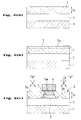
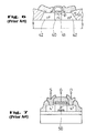
- Figs. 4(a) and 4(b) show a schematic cross section of a conventional MOSFET formed on a bulk Si and its equivalent electrical circuit, also showing a bipolar NPN transistor generated parasitically in this MOSFET structure.
- a gate electrode 23 is formed on a silicon substrate 20 with a gate oxide film 22 interposed therebetween, and source/drain regions 21 are formed in the silicon substrate 20. Therefore, a base terminal of the parasitic NPN bipolar transistor generated by the source/drain regions 21 and the silicon substrate 20 is tied to the substrate terminal, and the substrate/source junction is reverse biased. As a result, the bipolar NPN transistor has very little effect on the MOSFET operation.
- Figs. 5(a) and 5(b) show a schematic cross section of a conventional SOI ⁇ MOSFET and its equivalent electrical circuit, also showing a bipolar NPN transistor generated parasitically in this SOI ⁇ MOSFET structure.
- a silicon oxide film 32 and a top semiconductor layer are successively formed on a silicon substrate 31; a gate electrode 35 is formed on the top silicon layer with a gate oxide film 34 interposed therebetween; and source/drain regions 33 are formed in the top silicon layer. Therefore, a parasitic bipolar base is floating.
- holes generated by impact ionization at a drain junction could act as a base current for the parasitic bipolar NPN transistor, creating a positive feedback effect and degrading device electrical characteristics, especially short-channel effect and reduction of a drain/source breakdown voltage.
- the SOI ⁇ MOSFET with thick top Si channel it operates in the partially depleted mode, and holes generated by impact ionization flow into a neutral region under the channel, raising a channel potential to increase a drain current, which further increases the number of holes. This leads to a so-called "kink" effect in output characteristics, representing a serious limitation of the SOI ⁇ MOSFET.
- the present invention provides a SOI ⁇ MOSFET comprising: a substrate; a buried oxide film formed on the substrate; a top semiconductor layer formed on the buried oxide film; a gate electrode formed on the top semiconductor layer with a gate oxide film interposed therebetween; source/drain regions of a second conductivity type formed in the top semiconductor layer and on both sides of the gate electrode; and an embedded region of the second conductivity type disposed in the top semiconductor layer and between the source/drain regions and is separated from the source/drain regions and from a top semiconductor/gate oxide interface.
- the present invention provides a process of fabricating the above-mentioned SOI ⁇ MOSFET, comprising the steps of: (i) forming a buried oxide film and a top semiconductor layer of a second conductivity type successively on a substrate;(ii) implanting impurity ions of a first conductivity type into a surface of the top semiconductor layer thereafter; (iii) forming a gate electrode on the resultant substrate; and (iv) forming a deep channel portion of the first conductivity type underneath the gate electrode by a tilted implantation of impurity ions of the first conductivity type using the gate electrode as a mask to form an embedded region of the second conductivity type, before or after forming source/drain regions separated from the embedded region by implantation of impurity ions of the second conductivity type from above the substrate.
- the present invention provides with a SOI MOSFET structure with a fully depleted channel on a relatively thick top Si film.
- a substrate, a buried oxide film, and a top semiconductor layer in the SOI ⁇ MOSFET of the present invention are those generally used in fabricating a semiconductor device having a SOI ⁇ MOSFET structure.
- the substrate may be a semiconductor substrate such as silicon or germanium, a compound semiconductor such as GaAs or InGaAs, an insulating substrate such as sapphire, quartz, glass, plastic or the like.
- the substrate is provided thereon with a buried oxide film and a top semiconductor layer which are mentioned later.
- This substrate could be a bonded SOI (BSOI) or SIMOX (Separation by Implantation of Oxygen) type substrate.
- the buried oxide film may be formed of, for example, SiO 2 to a thickness satisfying a later-mentioned relationship.
- the thickness of the buried oxide film may be varied suitably in accordance with other conditions, as shown in the following formula.
- the specific thickness of the buried oxide film may be about 50 nm to about 400 nm.
- the top semiconductor layer is a semiconductor thin film functioning as an active layer for forming a transistor and may be formed to a thickness satisfying the later-mentioned relationship.
- the thickness of the top semiconductor layer may be varied suitably in accordance with other conditions, as shown in the following formula.
- the specific thickness of the top semiconductor layer may be, for example, about 100 nm to about 500 nm, more preferably about 100 to about 200 nm.
- a surface of the top semiconductor layer, in which a channel region of the transistor is formed, preferably has an impurity concentration satisfying the later-mentioned relationship so as to fully deplete the channel region and to control a threshold voltage.
- the impurity concentration of the top semiconductor layer surface may be varied suitably in accordance with other conditions, as shown in the following formula.
- the top semiconductor layer surface may be formed by implanting impurity ions of a first conductivity type at a dose of about 0.5 x 10 12 to about 3 x 10 12 ions/cm 2 so that a final impurity concentration of the top semiconductor layer surface will be about 5 x 10 16 to about 3 x 10 17 ions/cm 3 .
- a gate electrode is formed on the top semiconductor layer with a gate oxide film interposed therebetween; and, further, source/drain regions of a second conductivity type are formed in the top semiconductor layer and on both sides of the gate electrode to constitute the transistor.
- the gate oxide film may be formed to have a thickness such that it functions generally as a gate oxide film and satisfies the later-mentioned relationship.
- the thickness of the gate oxide film may be varied suitably in accordance with other conditions, as shown in the following formula.
- the specific thickness of the gate oxide film is preferably about 5 to about 10 nm, more preferably about 5 to about 8 nm.
- the gate electrode is preferably formed to a thickness of about 150 to about 300 nm with polysilicon, a silicide of a refractory metal such as W, Ta, Ti or Mo, a polycide of these silicides, a different metal or the like.
- the gate electrode may be provided with a sidewall spacer formed of an insulating film having a thickness of about 100 to about 200 nm to constrain the lateral diffusion of impurity ions which are implanted for forming the later-mentioned source/drain regions.
- the source/drain regions contain the impurity ions of the second conductivity type at a concentration of about 1 x 10 20 to about 1 x 10 21 ions/cm 3 .
- the source/drain regions may each include shallow extension regions which may have a concentration of a lower level as a LDD structure and are formed at an end of the source/drain region adjacent to the channel.
- the source/drain regions may each include regions which may have a concentration of the same level or a concentration of a higher level and may have a depth a little smaller than the junction depth of the source/drain regions.
- the SOI ⁇ MOSFET according to the present invention has an embedded region of the second conductivity type disposed between the source/drain regions in the top semiconductor layer and underneath the gate electrode and separated from the source/drain regions and from a top semiconductor/gate oxide interface.
- This embedded region is used to fully deplete the channel region by contact potential with the channel region, so that there is no need for the embedded region itself to be fully depleted.
- the embedded region may have a junction depth, an impurity concentration and the like that satisfy the later-mentioned relationship.
- the junction depth and the impurity concentration of the embedded region may vary suitably in accordance with other conditions, as shown in the following formula.
- the specific junction depth of the embedded region is preferably about 50 to about 450 nm if the top semiconductor layer has a thickness of about 100 to about 500 nm.
- the impurity concentration of the embedded region may be, for example, about 3 x 10 16 to about 1 x 10 18 ions/cm 3 .
- the embedded region is floating and in contact with the buried oxide/top semiconductor interface to be coupled to the substrate bias through capacitive coupling with the buried oxide film and the substrate.
- the embedded region is explained as a second conductivity type region, the embedded region is N-type in the case of an enhanced mode NMOSFET, and it is P-type in the case of an enhanced mode PMOSFET.
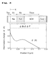
- the gate oxide thickness is Tox; the surface channel (P-type) has a doping level Na and a thickness Xc; and the embedded region has a thickness Xb and a doping level Nd.
- the buried oxide thickness is Tbox and the bias voltages are Vg and Vb for the gate electrode and the substrate, respectively.
- Vfb the top interface flat-band voltage
- ⁇ B 2 ⁇ F
- Cox ⁇ ox /Tox
- Cbox ⁇ ox /Tbox
- Cch ⁇ /Xc
- Cjb ⁇ /Xb
- Vb1 Vb - Vfbb
- Vfbb the back interface flat-band voltage.
- Cboxe 1 1 Cjb + 1 Cbox
- the surface channel is depleted from the gate oxide/top semiconductor interface by Xcs, and a depletion region extends from the buried PN junction (between the embedded region and the channel region) into the channel region by Xbp:
- Xcs [2 ⁇ ⁇ B/q Na] 1/2
- Xbp [2 ⁇ (Nd/Na)Vbi/q(Na + Nd)] 1/2 where Vbi is the PN junction built-in potential.
- a SOI substrate is used in which the top semiconductor layer is doped as to become a semiconductor film of the second conductivity type. This doping may be achieved by implanting impurity ions of the second conductivity type, followed by an annealing treatment under a desired condition.
- impurity ions of the first conductivity type are implanted into a surface of the top semiconductor layer in the step (ii).
- This implantation of the impurity ions of the first conductivity type is carried out uniformly on the entire surface of the top semiconductor layer in order to fully deplete the channel region and to control the threshold voltage of the channel region.
- the impurity ions are implanted preferably at an implantation energy of about 10 to about 20 keV, though it depends on the dose of the implantation, the thickness of the top semiconductor layer and the like.
- an annealing treatment is preferably carried out under an arbitrary condition.
- a gate electrode is formed on the resulting substrate in the step (iii).
- the gate electrode may be formed by depositing an electrically conductive material for the gate electrode to a desired thickness on the entire substrate and then patterning it to a desired shape by a known technique, for example, photolithography and etching method.
- a field oxide film is preferably formed by a LOCOS method or the like to define an active region before forming the gate electrode or before implanting impurity ions into the top semiconductor layer in the step (ii).
- impurity ions of the first conductivity type are implanted by a tilted implantation in the step (iv) using, as a mask, the gate electrode obtained in the above step.
- This implantation of the impurity ions is for forming a deep portion of the channel region adjacent to the later-mentioned source/drain regions and is preferably carried out with a tilted angle of about 30 to about 50° at an implantation energy adjusted to obtain an impurity concentration peak at around the center of the top semiconductor layer.
- the implantation energy may be about 30 to about 80 keV
- the implantation energy may be about 80 to about 150 keV.
- impurity ions of the second conductivity type are implanted from above the substrate using the gate electrode as a mask to form the source/drain regions.
- the tilted implantation may be carried out before the implantation from above the substrate, or vice versa.
- impurity ions of the second conductivity type may be implanted from above the substrate to form first portions of the source/drain regions and then sidewall spacers are formed adjacent to the gate electrode, impurity ions of the second conductivity type may be implanted from above the substrate using the gate electrode and the sidewall spacers as a mask to form second portions of the source/drain regions.
- impurity ions of the second conductivity type may be implanted from above the substrate to form first regions of the source/drain regions before the above-mentioned tilted implantation, and then, sidewall spacers are formed adjacent to the gate electrode, impurity ions of the second conductivity type may be implanted from above the substrate using the gate electrode and the sidewall spacers as a mask to form second portions of the source/drain regions.
- the first portions of the source/drain regions are shallow extension regions formed at an end of the source/drain regions adjacent to the channel and having a concentration of a lower level as a LDD structure.
- the first portions are regions having a concentration of the same level or a higher level and having a depth a little smaller than the junction depth of the second portions of the source/drain regions.
- source/drain regions By forming the source/drain regions through the two-step implantation of impurity ions, hot electrons generated at the end of the source/drain regions can be alleviated and the separation of the embedded region from the source/drain regions can be fully ensured, eliminating the need for additional margin in the fabricating process and further reducing the area occupied by the SOI ⁇ MOSFET.
- a salicide process may be carried out at least on the source/drain regions and further on the gate electrode. Namely, since the top semiconductor layer has a comparatively large thickness in the present invention, the salicide process can be carried out without penetrating through the top semiconductor layer.
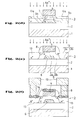
- the SOI ⁇ MOSFET of this embodiment is mainly composed of a silicon substrate 1, a buried oxide film 2, a top silicon layer 3, a gate insulating film 7, a gate electrode 4 with sidewall spacers 8, source/drain regions 13 of N-type having the LDD structure and an embedded region 6 of N-type.
- a channel region 5 having a fully depleted surface channel (P-type) with an impurity concentration adjusted according to the above formula is disposed between the source/drain regions 13 in the top silicon layer 3.
- the embedded region 6 is N-type which is the same conductivity type as the source/drain regions 13 and which is different from the conductivity type of the surface channel.
- the embedded region 6 is separated from the source/drain regions 13 and from the gate oxide/surface channel interface. Although the embedded region 6 is floating, the embedded region 6 is in contact with the buried oxide 2 and is capacitively coupled to the substrate potential through a capacitor formed by the embedded region 6, the buried oxide film 2 and the substrate 1.
- the contact potential between the surface channel (P-type) and the embedded region 6 is used to fully deplete the surface channel. As previously described, since the embedded region 6 is separated from the source/drain regions 13 by the channel region 5, there is no need for the embedded region 6 itself to be fully depleted.
- Fig. 2(a) refers to the starting SOI substrate to fabricate the SOI ⁇ MOSFET device of this embodiment.
- the SOI substrate may have been formed by any conventional technique such as SOS (Silicon On Sapphire), SIMOX (Silicon Separation by ion Implantation of Oxygen) and BSOI (Bonded SOI).
- the substrate 1 may be a semiconductor like silicon and the insulating layer 2 may be SiO 2 .
- a device isolation film (not shown) was formed on the resulting substrate 1 by LOCOS method to define an active region.
- a gate oxide film 7 was grown on the top silicon layer 3 to a thickness of about 7 nm by thermal oxidation.
- a polycrystalline silicon film was deposited as a gate electrode material to a thickness of about 200 nm by CVD method using a silane-based gas, as shown in Fig. 2(c).
- the gate electrode 4 was then patterned using a known photolithography and etching technique.
- P-type impurity ions such as 11 B + ions (i.e. of the same conductivity type as the surface channel 5a) were implanted into a comparatively deep portion of the top silicon layer 3 to form a P-type region 5b and to form an embedded region 6 of N-type having a thickness of about 50 nm under the surface channel 5a underneath the gate electrode 4.
- this implantation was done, for example, with a tilted angle of about 30 to 50° at an implantation energy of about 50 keV and a dose of about 7 x 10 12 to about 10 x 10 12 cm -2 so as to obtain an impurity concentration peak at around the center of the top silicon layer 3 and to reduce the short-channel effects.
- As + ions were implanted from above the silicon substrate 1 at an implantation energy of about 20 keV and a dose of about 2 x 10 14 cm -2 to form shallow low-concentration extension regions 13a of the N-type source/drain regions, as shown in Fig. 2(d).
- a CVD oxide is deposited to a thickness of about 100 to about 200 nm and etched back to form sidewall spacers 8, as shown in Fig. 2(e).
- As + ions were implanted at an implantation energy of about 40 keV and a dose of about 5 x 10 15 cm -2 to form high-concentration regions 13b of the source/drain regions, thereby forming the source/drain regions 13 with the LDD structure and forming the channel region 5. Proceeding in this way, the embedded region 6 was separated from the source/drain regions 13.
- the surfaces of the gate electrode 4 and the source/drain regions 13 were subjected to a salicide process to form a silicide layer 14, and a metal interconnection 15 was formed by a metallization process to complete the SOI ⁇ MOSFET.
- the present invention allows the formation of a SOI ⁇ MOSFET having a fully depleted surface channel on a comparatively thick top semiconductor layer, eliminating the conventional problem of "kink" effect. As a result, better control of the SOI ⁇ MOSFET electrical parameters is obtained, improving the manufacturing yield. Also, salicide process can be carried out in the metallization step. Further, integration process is facilitated and the process margin is enlarged, allowing to use a conventional etching technique.
- the present invention allows fabrication of the SOI ⁇ MOSFET without addition of complicated fabrication steps and facilitates the process control. Especially, if a two-step implantation of impurity ions is carried out in forming the source/drain regions, the process margin can be enlarged and the area occupied by the SOI ⁇ MOSFET can be further reduced.
Landscapes
- Thin Film Transistor (AREA)
Abstract
Description


Claims (11)
- A SOI·MOSFET comprising:a substrate;a buried oxide film formed on the substrate;a top semiconductor layer formed on the buried oxide film;a gate electrode formed on the top semiconductor layer with a gate oxide film interposed therebetween;source/drain regions of a second conductivity tape formed in the top semiconductor layer and on both sides of the gate electrode; andan embedded region of the second conductivity type which is disposed in the top semiconductor layer and between the source/drain regions and is separated from the source/drain regions and from a top semiconductor/gate oxide interface.
- The SOI·MOSFET of claim 1, in which the embedded region is formed adjacent to a buried oxide/top semiconductor interface.
- The SOI·MOSFET of claim 1 or 2, in which the embedded region is electrically floating.
- The SOi.MOSFET of claim 1, in which a surface of the top semiconductor layer is fully depleted by a depletion layer from the gate oxide/top semiconductor interface and a depletion layer from an embedded region top semiconductor interface.
- The SOI·MOSFET of claim 1, in which at least the source/drain regions include a salicide layer.
- The SOI·MOSFET of claim 1, in which sidewall spacers are formed on a sidewall of the gate electrode and the source/drain regions include shallow extension regions.
- A process of fabricating a SOI·MOSFET of claim 1 comprising the steps of:(i) forming a buried oxide film and a top semiconductor layer of a second conductivity type successively on a substrate;(ii) implanting impurity ions of a first conductivity type into a surface of the top semiconductor layer thereafter;(iii) forming a gate electrode on the resultant substrate; and(iv) forming a deep channel portion of the first conductivity type underneath the gate electrode by a tilted implantation of impurity ions of the first conductivity type using the gate electrode as a mask to form an embedded region of the second conductivity type, before or after forming source/drain regions separated from the embedded region by implantation of impurity ions of the second conductivity type from above the substrate.
- The process of fabricating a SOI·MOSFET of claim 7, in which the step (iv) comprises:(a) forming a deep channel portion of the first conductivity type underneath the gate electrode by a tilted implantation of impurity ions of the first conductivity type using the gate electrode as a mask to form an embedded region of the second conductivity type, before or after forming a first portion of the source/drain regions by implantation of impurity ions of the second conductivity type from above the substrate; and thereafter(b) forming sidewall spacers adjacent to the gate electrode and forming second portions of the source/drain regions by implantation of impurity ions of the second conductivity type from above the substrate using the gate electrode and the sidewall spacers as a mask.
- The process of fabricating a SOI·MOSFET of claim 7, in which the embedded region is formed adjacent to a buried oxide/top semiconductor interface.
- The process of fabricating a SOI·MOSFET of claim 7, in which the embedded region is formed into an electrically floating state.
- The process of fabricating a SOI·MOSFET of claim 7, in which a surface of the top semiconductor layer is formed so as to be fully depleted by a depletion layer from the gate oxide/top semiconductor interface and a depletion layer from an embedded region/top semiconductor interface.
Applications Claiming Priority (3)
| Application Number | Priority Date | Filing Date | Title |
|---|---|---|---|
| JP24148297A JP3337953B2 (en) | 1997-09-05 | 1997-09-05 | SOI MOSFET and manufacturing method thereof |
| JP241482/97 | 1997-09-05 | ||
| JP24148297 | 1997-09-05 |
Publications (2)
| Publication Number | Publication Date |
|---|---|
| EP0902482A1 true EP0902482A1 (en) | 1999-03-17 |
| EP0902482B1 EP0902482B1 (en) | 2003-09-17 |
Family
ID=17074977
Family Applications (1)
| Application Number | Title | Priority Date | Filing Date |
|---|---|---|---|
| EP98305138A Expired - Lifetime EP0902482B1 (en) | 1997-09-05 | 1998-06-29 | SOI-MOSFET and fabrication process thereof |
Country Status (6)
| Country | Link |
|---|---|
| US (1) | US6288425B1 (en) |
| EP (1) | EP0902482B1 (en) |
| JP (1) | JP3337953B2 (en) |
| KR (1) | KR100329055B1 (en) |
| DE (1) | DE69818183T2 (en) |
| TW (1) | TW500258U (en) |
Cited By (3)
| Publication number | Priority date | Publication date | Assignee | Title |
|---|---|---|---|---|
| US6429055B2 (en) * | 2000-06-30 | 2002-08-06 | Hynix Semiconductor Inc. | Method for making SOI MOSFETS |
| WO2003032401A1 (en) * | 2001-10-02 | 2003-04-17 | Nec Corporation | Semiconductor device and its manufacturing method |
| EP1739738A3 (en) * | 2005-06-30 | 2009-04-01 | STMicroelectronics (Crolles 2) SAS | Memory cell with an isolated-body MOS transistor with reinforced memory effect |
Families Citing this family (25)
| Publication number | Priority date | Publication date | Assignee | Title |
|---|---|---|---|---|
| US6156589A (en) * | 1998-09-03 | 2000-12-05 | Micron Technology, Inc. | Compact SOI body contact link |
| US6740912B1 (en) * | 1999-06-24 | 2004-05-25 | Agere Systems Inc. | Semiconductor device free of LLD regions |
| US6362082B1 (en) * | 1999-06-28 | 2002-03-26 | Intel Corporation | Methodology for control of short channel effects in MOS transistors |
| JP3573056B2 (en) * | 1999-07-16 | 2004-10-06 | セイコーエプソン株式会社 | Semiconductor device, semiconductor gate array, electro-optical device, and electronic equipment |
| JP2001036092A (en) | 1999-07-23 | 2001-02-09 | Mitsubishi Electric Corp | Semiconductor device |
| KR100343288B1 (en) * | 1999-10-25 | 2002-07-15 | 윤종용 | An SOI semiconductor integrated circuit for eliminating floating body effect in SOI MOSFETs and method of fabricating the same |
| US6521959B2 (en) | 1999-10-25 | 2003-02-18 | Samsung Electronics Co., Ltd. | SOI semiconductor integrated circuit for eliminating floating body effects in SOI MOSFETs and method of fabricating the same |
| JP3608456B2 (en) * | 1999-12-08 | 2005-01-12 | セイコーエプソン株式会社 | Manufacturing method of SOI structure MIS field effect transistor |
| JP3504212B2 (en) * | 2000-04-04 | 2004-03-08 | シャープ株式会社 | Semiconductor device with SOI structure |
| US6512269B1 (en) * | 2000-09-07 | 2003-01-28 | International Business Machines Corporation | High-voltage high-speed SOI MOSFET |
| US6479866B1 (en) * | 2000-11-14 | 2002-11-12 | Advanced Micro Devices, Inc. | SOI device with self-aligned selective damage implant, and method |
| CN1147935C (en) * | 2000-12-18 | 2004-04-28 | 黄敞 | Complementary Even-Carrier Field Effect Transistor and Its System-on-Chip |
| JP2002185008A (en) * | 2000-12-19 | 2002-06-28 | Hitachi Ltd | Thin film transistor |
| US6538284B1 (en) * | 2001-02-02 | 2003-03-25 | Advanced Micro Devices, Inc. | SOI device with body recombination region, and method |
| US6509613B1 (en) * | 2001-05-04 | 2003-01-21 | Advanced Micro Devices, Inc. | Self-aligned floating body control for SOI device through leakage enhanced buried oxide |
| US7122863B1 (en) | 2001-05-07 | 2006-10-17 | Advanced Micro Devices, Inc. | SOI device with structure for enhancing carrier recombination and method of fabricating same |
| US6528851B1 (en) * | 2001-05-31 | 2003-03-04 | Advanced Micro Devices, Inc. | Post-silicidation implant for introducing recombination center in body of SOI MOSFET |
| US6407428B1 (en) * | 2001-06-15 | 2002-06-18 | Advanced Micro Devices, Inc. | Field effect transistor with a buried and confined metal plate to control short channel effects |
| US6828632B2 (en) * | 2002-07-18 | 2004-12-07 | Micron Technology, Inc. | Stable PD-SOI devices and methods |
| KR100985581B1 (en) | 2003-04-30 | 2010-10-06 | 매그나칩 반도체 유한회사 | Semiconductor device and manufacturing method |
| KR100650901B1 (en) * | 2005-12-29 | 2006-11-28 | 동부일렉트로닉스 주식회사 | Metal oxide semiconductor transistor with buried gate |
| DE102005063092B3 (en) * | 2005-12-30 | 2007-07-19 | Advanced Micro Devices, Inc., Sunnyvale | Semiconductor device having a contact structure with increased Ätzselektivität |
| US7704844B2 (en) * | 2007-10-04 | 2010-04-27 | International Business Machines Corporation | High performance MOSFET |
| GB201202128D0 (en) * | 2012-02-08 | 2012-03-21 | Univ Leeds | Novel material |
| CN113363323B (en) * | 2020-03-05 | 2023-08-18 | 苏州大学 | Single gate field effect transistor device and method for regulating and controlling driving current thereof |
Citations (7)
| Publication number | Priority date | Publication date | Assignee | Title |
|---|---|---|---|---|
| JPS5678156A (en) * | 1979-11-30 | 1981-06-26 | Fujitsu Ltd | Charge pump semiconductor memory |
| JPS62133762A (en) * | 1985-12-06 | 1987-06-16 | Hitachi Ltd | semiconductor equipment |
| JPH02178965A (en) * | 1988-12-29 | 1990-07-11 | Nippondenso Co Ltd | Insulated isolation type field-effect semiconductor device |
| US4965213A (en) * | 1988-02-01 | 1990-10-23 | Texas Instruments Incorporated | Silicon-on-insulator transistor with body node to source node connection |
| JPH05218425A (en) * | 1992-01-31 | 1993-08-27 | Nippon Telegr & Teleph Corp <Ntt> | Field effect semiconductor device and manufacturing method thereof |
| US5296727A (en) * | 1990-08-24 | 1994-03-22 | Fujitsu Limited | Double gate FET and process for manufacturing same |
| US5463237A (en) * | 1993-11-04 | 1995-10-31 | Victor Company Of Japan, Ltd. | MOSFET device having depletion layer |
Family Cites Families (3)
| Publication number | Priority date | Publication date | Assignee | Title |
|---|---|---|---|---|
| US4563805A (en) * | 1984-03-08 | 1986-01-14 | Standard Telephones And Cables, Plc | Manufacture of MOSFET with metal silicide contact |
| TW222345B (en) * | 1992-02-25 | 1994-04-11 | Semicondustor Energy Res Co Ltd | Semiconductor and its manufacturing method |
| JP3222380B2 (en) | 1996-04-25 | 2001-10-29 | シャープ株式会社 | Field effect transistor and CMOS transistor |
-
1997
- 1997-09-05 JP JP24148297A patent/JP3337953B2/en not_active Expired - Fee Related
-
1998
- 1998-06-18 US US09/099,107 patent/US6288425B1/en not_active Expired - Lifetime
- 1998-06-18 TW TW090216904U patent/TW500258U/en not_active IP Right Cessation
- 1998-06-29 EP EP98305138A patent/EP0902482B1/en not_active Expired - Lifetime
- 1998-06-29 DE DE69818183T patent/DE69818183T2/en not_active Expired - Fee Related
- 1998-07-02 KR KR1019980026541A patent/KR100329055B1/en not_active Expired - Fee Related
Patent Citations (7)
| Publication number | Priority date | Publication date | Assignee | Title |
|---|---|---|---|---|
| JPS5678156A (en) * | 1979-11-30 | 1981-06-26 | Fujitsu Ltd | Charge pump semiconductor memory |
| JPS62133762A (en) * | 1985-12-06 | 1987-06-16 | Hitachi Ltd | semiconductor equipment |
| US4965213A (en) * | 1988-02-01 | 1990-10-23 | Texas Instruments Incorporated | Silicon-on-insulator transistor with body node to source node connection |
| JPH02178965A (en) * | 1988-12-29 | 1990-07-11 | Nippondenso Co Ltd | Insulated isolation type field-effect semiconductor device |
| US5296727A (en) * | 1990-08-24 | 1994-03-22 | Fujitsu Limited | Double gate FET and process for manufacturing same |
| JPH05218425A (en) * | 1992-01-31 | 1993-08-27 | Nippon Telegr & Teleph Corp <Ntt> | Field effect semiconductor device and manufacturing method thereof |
| US5463237A (en) * | 1993-11-04 | 1995-10-31 | Victor Company Of Japan, Ltd. | MOSFET device having depletion layer |
Non-Patent Citations (4)
| Title |
|---|
| PATENT ABSTRACTS OF JAPAN vol. 005, no. 145 (E - 074) 12 September 1981 (1981-09-12) * |
| PATENT ABSTRACTS OF JAPAN vol. 011, no. 359 (E - 559) 21 November 1987 (1987-11-21) * |
| PATENT ABSTRACTS OF JAPAN vol. 014, no. 448 (E - 0983) 26 September 1990 (1990-09-26) * |
| PATENT ABSTRACTS OF JAPAN vol. 017, no. 657 (E - 1470) 6 December 1993 (1993-12-06) * |
Cited By (4)
| Publication number | Priority date | Publication date | Assignee | Title |
|---|---|---|---|---|
| US6429055B2 (en) * | 2000-06-30 | 2002-08-06 | Hynix Semiconductor Inc. | Method for making SOI MOSFETS |
| WO2003032401A1 (en) * | 2001-10-02 | 2003-04-17 | Nec Corporation | Semiconductor device and its manufacturing method |
| US7485923B2 (en) | 2001-10-02 | 2009-02-03 | Nec Corporation | SOI semiconductor device with improved halo region and manufacturing method of the same |
| EP1739738A3 (en) * | 2005-06-30 | 2009-04-01 | STMicroelectronics (Crolles 2) SAS | Memory cell with an isolated-body MOS transistor with reinforced memory effect |
Also Published As
| Publication number | Publication date |
|---|---|
| TW500258U (en) | 2002-08-21 |
| EP0902482B1 (en) | 2003-09-17 |
| US6288425B1 (en) | 2001-09-11 |
| KR100329055B1 (en) | 2002-08-21 |
| KR19990029240A (en) | 1999-04-26 |
| JPH1187719A (en) | 1999-03-30 |
| DE69818183T2 (en) | 2004-06-03 |
| DE69818183D1 (en) | 2003-10-23 |
| JP3337953B2 (en) | 2002-10-28 |
Similar Documents
| Publication | Publication Date | Title |
|---|---|---|
| EP0902482B1 (en) | SOI-MOSFET and fabrication process thereof | |
| KR100259181B1 (en) | Field Effect Transistors and CMOS Devices | |
| US5185280A (en) | Method of fabricating a soi transistor with pocket implant and body-to-source (bts) contact | |
| KR100252866B1 (en) | Semiconductor device and manufacturing method thereof | |
| US5144390A (en) | Silicon-on insulator transistor with internal body node to source node connection | |
| KR100259097B1 (en) | Semiconductor device and method for fabricating the same | |
| EP0480635B1 (en) | Thin film transistor and a method of manufacturing thereof | |
| US7192816B2 (en) | Self-aligned body tie for a partially depleted SOI device structure | |
| US6770517B2 (en) | Semiconductor device and method for fabricating the same | |
| US6579750B1 (en) | Manufacturing method for fully depleted silicon on insulator semiconductor device | |
| US6462379B2 (en) | SOI semiconductor device and method for manufacturing the same | |
| US6509613B1 (en) | Self-aligned floating body control for SOI device through leakage enhanced buried oxide | |
| US8354714B2 (en) | SOI MOS device having BTS structure and manufacturing method thereof | |
| JP3103159B2 (en) | Semiconductor device | |
| EP1229576B1 (en) | Method of producing SOI MOSFET | |
| US6130135A (en) | Method of fabricating lightly-doped drain transistor having inverse-T gate structure | |
| US6512244B1 (en) | SOI device with structure for enhancing carrier recombination and method of fabricating same | |
| US7122863B1 (en) | SOI device with structure for enhancing carrier recombination and method of fabricating same | |
| US6420767B1 (en) | Capacitively coupled DTMOS on SOI | |
| US7968415B2 (en) | Transistor with reduced short channel effects and method | |
| US8354310B2 (en) | SOI MOS device having a source/body ohmic contact and manufacturing method thereof | |
| CN100416839C (en) | Partially depleted SOI MOS device | |
| JP2007123519A (en) | Semiconductor device manufacturing method and semiconductor device | |
| JPH06151842A (en) | Semiconductor device and its manufacture | |
| JP2000223721A (en) | High breakdown voltage semiconductor device and method of manufacturing the same |
Legal Events
| Date | Code | Title | Description |
|---|---|---|---|
| PUAI | Public reference made under article 153(3) epc to a published international application that has entered the european phase |
Free format text: ORIGINAL CODE: 0009012 |
|
| AK | Designated contracting states |
Kind code of ref document: A1 Designated state(s): DE FR GB NL |
|
| AX | Request for extension of the european patent |
Free format text: AL;LT;LV;MK;RO;SI |
|
| 17P | Request for examination filed |
Effective date: 19990702 |
|
| AKX | Designation fees paid |
Free format text: DE FR GB NL |
|
| 17Q | First examination report despatched |
Effective date: 20000320 |
|
| GRAG | Despatch of communication of intention to grant |
Free format text: ORIGINAL CODE: EPIDOS AGRA |
|
| GRAG | Despatch of communication of intention to grant |
Free format text: ORIGINAL CODE: EPIDOS AGRA |
|
| GRAG | Despatch of communication of intention to grant |
Free format text: ORIGINAL CODE: EPIDOS AGRA |
|
| GRAH | Despatch of communication of intention to grant a patent |
Free format text: ORIGINAL CODE: EPIDOS IGRA |
|
| GRAS | Grant fee paid |
Free format text: ORIGINAL CODE: EPIDOSNIGR3 |
|
| GRAA | (expected) grant |
Free format text: ORIGINAL CODE: 0009210 |
|
| AK | Designated contracting states |
Kind code of ref document: B1 Designated state(s): DE FR GB NL |
|
| REG | Reference to a national code |
Ref country code: GB Ref legal event code: FG4D |
|
| REF | Corresponds to: |
Ref document number: 69818183 Country of ref document: DE Date of ref document: 20031023 Kind code of ref document: P |
|
| ET | Fr: translation filed | ||
| PLBE | No opposition filed within time limit |
Free format text: ORIGINAL CODE: 0009261 |
|
| STAA | Information on the status of an ep patent application or granted ep patent |
Free format text: STATUS: NO OPPOSITION FILED WITHIN TIME LIMIT |
|
| 26N | No opposition filed |
Effective date: 20040618 |
|
| PGFP | Annual fee paid to national office [announced via postgrant information from national office to epo] |
Ref country code: NL Payment date: 20080603 Year of fee payment: 11 Ref country code: DE Payment date: 20080703 Year of fee payment: 11 |
|
| PGFP | Annual fee paid to national office [announced via postgrant information from national office to epo] |
Ref country code: FR Payment date: 20080617 Year of fee payment: 11 |
|
| PGFP | Annual fee paid to national office [announced via postgrant information from national office to epo] |
Ref country code: GB Payment date: 20080702 Year of fee payment: 11 |
|
| GBPC | Gb: european patent ceased through non-payment of renewal fee |
Effective date: 20090629 |
|
| NLV4 | Nl: lapsed or anulled due to non-payment of the annual fee |
Effective date: 20100101 |
|
| REG | Reference to a national code |
Ref country code: FR Ref legal event code: ST Effective date: 20100226 |
|
| PG25 | Lapsed in a contracting state [announced via postgrant information from national office to epo] |
Ref country code: FR Free format text: LAPSE BECAUSE OF NON-PAYMENT OF DUE FEES Effective date: 20090630 |
|
| PG25 | Lapsed in a contracting state [announced via postgrant information from national office to epo] |
Ref country code: GB Free format text: LAPSE BECAUSE OF NON-PAYMENT OF DUE FEES Effective date: 20090629 |
|
| PG25 | Lapsed in a contracting state [announced via postgrant information from national office to epo] |
Ref country code: DE Free format text: LAPSE BECAUSE OF NON-PAYMENT OF DUE FEES Effective date: 20100101 |
|
| PG25 | Lapsed in a contracting state [announced via postgrant information from national office to epo] |
Ref country code: NL Free format text: LAPSE BECAUSE OF NON-PAYMENT OF DUE FEES Effective date: 20100101 |