EP0901645B1 - Elektrooptisches modul - Google Patents
Elektrooptisches modul Download PDFInfo
- Publication number
- EP0901645B1 EP0901645B1 EP97924908A EP97924908A EP0901645B1 EP 0901645 B1 EP0901645 B1 EP 0901645B1 EP 97924908 A EP97924908 A EP 97924908A EP 97924908 A EP97924908 A EP 97924908A EP 0901645 B1 EP0901645 B1 EP 0901645B1
- Authority
- EP
- European Patent Office
- Prior art keywords
- electro
- substrate
- optical
- component
- optical module
- Prior art date
- Legal status (The legal status is an assumption and is not a legal conclusion. Google has not performed a legal analysis and makes no representation as to the accuracy of the status listed.)
- Expired - Lifetime
Links
- 239000000758 substrate Substances 0.000 claims description 31
- 239000013307 optical fiber Substances 0.000 claims description 5
- 230000003287 optical effect Effects 0.000 description 6
- 239000004020 conductor Substances 0.000 description 4
- 239000000835 fiber Substances 0.000 description 4
- 238000004519 manufacturing process Methods 0.000 description 4
- 238000001465 metallisation Methods 0.000 description 4
- 239000002184 metal Substances 0.000 description 3
- XUIMIQQOPSSXEZ-UHFFFAOYSA-N Silicon Chemical compound [Si] XUIMIQQOPSSXEZ-UHFFFAOYSA-N 0.000 description 2
- 238000010276 construction Methods 0.000 description 2
- 238000005516 engineering process Methods 0.000 description 2
- 229910052710 silicon Inorganic materials 0.000 description 2
- 239000010703 silicon Substances 0.000 description 2
- 229910000679 solder Inorganic materials 0.000 description 2
- WZZBNLYBHUDSHF-DHLKQENFSA-N 1-[(3s,4s)-4-[8-(2-chloro-4-pyrimidin-2-yloxyphenyl)-7-fluoro-2-methylimidazo[4,5-c]quinolin-1-yl]-3-fluoropiperidin-1-yl]-2-hydroxyethanone Chemical compound CC1=NC2=CN=C3C=C(F)C(C=4C(=CC(OC=5N=CC=CN=5)=CC=4)Cl)=CC3=C2N1[C@H]1CCN(C(=O)CO)C[C@@H]1F WZZBNLYBHUDSHF-DHLKQENFSA-N 0.000 description 1
- 206010020751 Hypersensitivity Diseases 0.000 description 1
- 208000026935 allergic disease Diseases 0.000 description 1
- 230000005540 biological transmission Effects 0.000 description 1
- 238000012937 correction Methods 0.000 description 1
- 230000008878 coupling Effects 0.000 description 1
- 238000010168 coupling process Methods 0.000 description 1
- 238000005859 coupling reaction Methods 0.000 description 1
- 230000003247 decreasing effect Effects 0.000 description 1
- 238000013461 design Methods 0.000 description 1
- 238000011161 development Methods 0.000 description 1
- 238000005530 etching Methods 0.000 description 1
- 238000011156 evaluation Methods 0.000 description 1
- 230000002349 favourable effect Effects 0.000 description 1
- 230000009610 hypersensitivity Effects 0.000 description 1
- 238000009434 installation Methods 0.000 description 1
- 239000000463 material Substances 0.000 description 1
- 238000000034 method Methods 0.000 description 1
- 238000003303 reheating Methods 0.000 description 1
- 230000008054 signal transmission Effects 0.000 description 1
- 239000002210 silicon-based material Substances 0.000 description 1
Images

Classifications
-
- G—PHYSICS
- G02—OPTICS
- G02B—OPTICAL ELEMENTS, SYSTEMS OR APPARATUS
- G02B6/00—Light guides; Structural details of arrangements comprising light guides and other optical elements, e.g. couplings
- G02B6/24—Coupling light guides
- G02B6/42—Coupling light guides with opto-electronic elements
- G02B6/4201—Packages, e.g. shape, construction, internal or external details
- G02B6/4274—Electrical aspects
- G02B6/4277—Protection against electromagnetic interference [EMI], e.g. shielding means
-
- G—PHYSICS
- G02—OPTICS
- G02B—OPTICAL ELEMENTS, SYSTEMS OR APPARATUS
- G02B6/00—Light guides; Structural details of arrangements comprising light guides and other optical elements, e.g. couplings
- G02B6/24—Coupling light guides
- G02B6/42—Coupling light guides with opto-electronic elements
- G02B6/4201—Packages, e.g. shape, construction, internal or external details
- G02B6/4204—Packages, e.g. shape, construction, internal or external details the coupling comprising intermediate optical elements, e.g. lenses, holograms
-
- G—PHYSICS
- G02—OPTICS
- G02B—OPTICAL ELEMENTS, SYSTEMS OR APPARATUS
- G02B6/00—Light guides; Structural details of arrangements comprising light guides and other optical elements, e.g. couplings
- G02B6/24—Coupling light guides
- G02B6/42—Coupling light guides with opto-electronic elements
- G02B6/4292—Coupling light guides with opto-electronic elements the light guide being disconnectable from the opto-electronic element, e.g. mutually self aligning arrangements
Definitions
- the invention is in the field of electro-optical structures for optical systems and concerns an electro-optical module with an electro-optical component and with a holder for a fiber optic connector that is on a single Surface of a substrate are arranged, and with an in arranged optical path between the component and the receptacle Lens.
- Such modules are used for signal transmission by means of optical Waveguides and contain at least one component, which comprises an electro-optical converter.
- An electro-optical Converter is used to convert optical to electrical signals or vice versa to convert electrical to optical Signals.
- a module of the type mentioned above is from the EP 0 600 645 A1 and comprises two electro-optical components (Laser diode and photodiode) that are precise on one Silicon substrate placed metal surfaces ("pads") with re-heatable Plumb to be positioned.
- the components are due to reheating the solder (reflow) compared to the surface tension of the liquefied solder centered on the metal surfaces.
- the electro-optical Components is in the silicon material by etching created a variety of alignment wells.
- alignment elements for example alignment balls - insertable, with corresponding alignment recesses a separate one, above the respective electro-optical Cooperate component precisely aligned carrier.
- the carrier can be in the beam path between the component and a receptacle for an optical fiber connector Wear lens or relate directly to the shot align with the component.
- the carrier With extremely precise manufacture of the individual parts, in particular the carrier, the two-part alignment recesses and possibly the lens or the receptacle for the fiber optic connector, enables the known module to an active one Adjustment of the receptacle in relation to the electro-optical component to renounce.
- the height of the carrier and possibly the lens diameter are, however, constructive quantities that relate to the relative Position of the receptacle or the fiber optic connector compared to the electro-optical component in the Z direction - So in the direction of the optical fiber or beam path - have significant influence.
- the invention has for its object an electro-optical To create a module with as few individual parts as possible high-precision, reproducible coupling geometries in the Z direction having.
- the substrate is therefore not special Structuring properties - such as the silicon substrate to be used according to EP 0 600 645 A1 - reliant. Rather, the substrate (e.g. printed circuit board) according to handling, manufacturing and especially be selected in an optimized manner from a cost perspective.
- the substrate e.g. printed circuit board
- Another important advantage of the invention is in that the of the electro-optical component and Lens-formed surface-mountable assembly in advance with high precision can be manufactured and tested.
- the structural unit can preferably be metallic Surfaces for direct electrical contact with have the substrate. The reproducible accuracy in the Z direction is only determined by the unit while advantageously not the substrate thickness in this regard is relevant.
- a preferred embodiment of the module according to the invention is that the recording contactless to the unit is arranged and only with the surface of the substrate in contact and connected. This construction enables a completely tension-free and with temperature changes hardly burdened design.
- the substrate its side facing away from the recording is an electronic one Circuit carries.
- the high-frequency properties and the insensitivity to further improve against external disturbances sees a preferred development of the invention Module that the integrated unit through an immediate cap applied to the surface of the substrate is electrically shielded.
- Another advantageous embodiment provides that the Substrate part of a rigid-flex-rigid circuit carrier is.
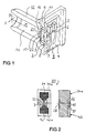
- the electro-optical module contains a substrate in the form of a printed circuit board 1, on its front flat side (first surface) 2 u. a. an electro-optical component 3 is arranged.
- On the rear surface 4 of the substrate 1 are suggestive individual electronic components 5, 6, which are interconnected via conductor tracks 7 interconnected and by not shown electrical Bushings through the substrate 1 with connection contact surfaces 8, 9 are connected on the first surface 2.
- the connection contact surfaces are used to contact the electro-optical Component 3.
- a flange 10 from a receptacle 12, which is a central Bore 14 for receiving a not known per se contains optical fiber connector shown.
- the one Light path between the electro-optical component 3 and one centrally recorded in the fiber optic connector Optical fiber end enables.
- the component 3 forms an integral part one mounted on the surface 2 of the substrate 1 Unit 20.
- the top 22 of the assembly 20 remote from the substrate is as Shaped lens (see. Figure 2), thus in the optical path lies between the component and the receptacle 12.
- the surface 2 has the mentioned contact surfaces 8, 9 and is otherwise not mechanically structured; it contains in particular no alignment recesses for the assembly 20.
- FIG. 2 shows in a top view and a sectional view the assembly 20 is an integral unit from the top 22 trained lens 28 and electro-optical component 3.
- the component 3 is hermetic for protection against external influences tightly embedded in a filling compound 30, which also for contacting the component 3 on its top attached bond wire 32 includes.
- the bond wire 32 leads to a connection metallization 34, which extends over a slope and the floor area a recess 40 receiving the component 3 extends.
- the bottom of the component 3 is with a second metallization 42 electrically connected.
- the receptacle 12 is non-contact is arranged to the unit 20 and only with the surface 2 of the substrate 1 in contact and connected is. This allows a particularly low-voltage and temperature change insensitive to the structure of the module to reach. Furthermore, one is directly on the surface 2 applied electrically conductive cap 60 recognizable by the module 20 is electrically shielded on the receiving side is.
- the module described above an adjustment of the Recording 12 with respect to component 3 in the X-Y direction - d. H. in the plane perpendicular to the Z direction - required but because of the smooth and evenly formed circuit board surface 2 is easily possible.
- the module offers the main advantage that only comparatively few Tolerances affect the accuracy in the Z direction, so that no adjustments or corrections in this regard after installation Measures are more necessary.
- Another advantage of the module is that the assembly 20 and the Recording 12 on the same reference surface - namely the surface 2 - are aligned in the Z direction. The precision in the Z direction is essentially only a only part, namely the assembly 20, determines while the substrate thickness is not considered.
- the evaluation or Control electronics for the component 3 can be arranged on the back of the substrate.
- the evaluation or Control electronics for the component 3 can be arranged.
- Through short conductor tracks 7 and direct plated-through holes to unit 20 are favorable high-frequency properties and high insensitivity to external Guaranteed interference.
- the hypersensitivity is caused by the appropriately contacted cap 6 still increased.
- FIG 3 is a rigid-flex-rigid circuit carrier in a perspective view 50 shown made of a rigid part 1, formed by the substrate, having a flexible part 51 flexible conductors and another rigid part 52.
- the circuit carrier 50 can be assembled as a unit can be mounted, which saves mounting steps become.
Landscapes
- Physics & Mathematics (AREA)
- General Physics & Mathematics (AREA)
- Optics & Photonics (AREA)
- Electromagnetism (AREA)
- Optical Couplings Of Light Guides (AREA)
Description
Claims (5)
- Elektrooptisches Moduldadurch gekennzeichnet, daßmit einem elektrooptischen Bauelement (3) und mit einer Aufnahme (12) für einen Lichtwellenleiterstecker, die auf derselben Montage-Oberfläche (2) eines Substrats (1) angeordnet sind, undmit einer im Strahlengang zwischen dem Bauelement (3) und der Aufnahme (12) angeordneten Linse (28),wobei die Montage-Oberfläche (2) senkrecht zum Strahlengang orientiert ist,die Montage-Oberfläche (2) frei von Ausrichtstrukturen ist und daßdas elektrooptische Bauelement (3) und die Linse (28) unmittelbar aufeinander ausgerichtet sind und eine integrierte, auf der Montage-Oberfläche (2) montierte Baueinheit (20) bilden.
- Elektrooptisches Modul nach Anspruch 1,
dadurch gekennzeichnet, daß
die Aufnahme (12) berührungsfrei zu der Baueinheit (20) angeordnet ist und nur mit der Oberfläche (2) des Substrats (1) in Kontakt und verbunden ist. - Elektrooptisches Modul nach Anspruch 1 oder 2,
dadurch gekennzeichnet, daß
das Substrat (1) auf seiner der Aufnahme (12) abgewandten Seite eine elektronische Schaltung trägt. - Elektrooptisches Modul nach Anspruch 1 oder 2,
dadurch gekennzeichnet, daß
die Baueinheit (20) durch eine unmittelbar auf die Oberfläche (2) des Substrats (1) aufgebrachte Kappe (60) elektrisch abgeschirmt ist. - Elektrooptisches Modul nach Anspruch 1 oder einem der folgenden,
dadurch gekennzeichnet, daß
das Substrat (1) ein Teil eines Starr-flex-starr-Schaltungsträgers (50) ist.
Applications Claiming Priority (3)
| Application Number | Priority Date | Filing Date | Title |
|---|---|---|---|
| DE19622459A DE19622459C1 (de) | 1996-05-24 | 1996-05-24 | Elektrooptisches Modul |
| DE19622459 | 1996-05-24 | ||
| PCT/DE1997/001041 WO1997045759A1 (de) | 1996-05-24 | 1997-05-16 | Elektrooptisches modul |
Publications (2)
| Publication Number | Publication Date |
|---|---|
| EP0901645A1 EP0901645A1 (de) | 1999-03-17 |
| EP0901645B1 true EP0901645B1 (de) | 2001-08-16 |
Family
ID=25962905
Family Applications (1)
| Application Number | Title | Priority Date | Filing Date |
|---|---|---|---|
| EP97924908A Expired - Lifetime EP0901645B1 (de) | 1996-05-24 | 1997-05-16 | Elektrooptisches modul |
Country Status (4)
| Country | Link |
|---|---|
| EP (1) | EP0901645B1 (de) |
| JP (1) | JP2000510963A (de) |
| DE (2) | DE19622459C1 (de) |
| WO (1) | WO1997045759A1 (de) |
Families Citing this family (6)
| Publication number | Priority date | Publication date | Assignee | Title |
|---|---|---|---|---|
| DE19846213C1 (de) * | 1998-10-07 | 1999-10-28 | Siemens Ag | Optisches Modul |
| DE19910164C2 (de) * | 1999-02-24 | 2002-10-17 | Infineon Technologies Ag | Elektrooptisches Modul |
| DE19946101A1 (de) | 1999-09-22 | 2001-05-03 | Infineon Technologies Ag | Elektrooptisches Modul mit einem Gehäuse |
| US7327022B2 (en) | 2002-12-30 | 2008-02-05 | General Electric Company | Assembly, contact and coupling interconnection for optoelectronics |
| DE10322757B4 (de) * | 2003-05-19 | 2012-08-30 | Avago Technologies Fiber Ip (Singapore) Pte. Ltd. | Optoelektronische Sende- und/oder Empfangsanordnungen |
| DE102010011161A1 (de) * | 2010-03-12 | 2011-09-15 | Siemens Aktiengesellschaft | Sensorsystem zur Erfassung der Bewegung eines Objekts |
Family Cites Families (6)
| Publication number | Priority date | Publication date | Assignee | Title |
|---|---|---|---|---|
| EP0053482B1 (de) * | 1980-11-28 | 1987-03-04 | Kabushiki Kaisha Toshiba | Modul für einen fiberoptischen Anschluss |
| US4995695A (en) * | 1989-08-17 | 1991-02-26 | At&T Bell Laboratories | Optical assembly comprising optical fiber coupling means |
| US4979787A (en) * | 1990-01-12 | 1990-12-25 | Pco, Inc. | Optical-electronic interface module |
| US5259053A (en) * | 1992-06-29 | 1993-11-02 | The Whitaker Corporation | Discrete optical receptacle assembly with alignment feature |
| GB9223306D0 (en) * | 1992-11-06 | 1992-12-23 | Bt & D Technologies Ltd | Optoelectronic devices |
| US5337398A (en) * | 1992-11-30 | 1994-08-09 | At&T Bell Laboratories | Single in-line optical package |
-
1996
- 1996-05-24 DE DE19622459A patent/DE19622459C1/de not_active Expired - Fee Related
-
1997
- 1997-05-16 WO PCT/DE1997/001041 patent/WO1997045759A1/de not_active Ceased
- 1997-05-16 EP EP97924908A patent/EP0901645B1/de not_active Expired - Lifetime
- 1997-05-16 DE DE59704315T patent/DE59704315D1/de not_active Expired - Fee Related
- 1997-05-16 JP JP09541389A patent/JP2000510963A/ja active Pending
Also Published As
| Publication number | Publication date |
|---|---|
| DE19622459C1 (de) | 1997-11-27 |
| JP2000510963A (ja) | 2000-08-22 |
| DE59704315D1 (de) | 2001-09-20 |
| EP0901645A1 (de) | 1999-03-17 |
| WO1997045759A1 (de) | 1997-12-04 |
Similar Documents
| Publication | Publication Date | Title |
|---|---|---|
| DE69525701T2 (de) | Integrierter optoelektronischer Verbund und Stecker | |
| DE69018287T2 (de) | Verpackungstechniken für optische Sender/Empfänger. | |
| DE3687063T2 (de) | Optische komponente mit wellenleiter. | |
| DE10034865B4 (de) | Optoelektronisches oberflächenmontierbares Modul | |
| DE69708328T2 (de) | Steckerteil zum direkten ankoppeln optoelektronischer elemente | |
| EP3627545A2 (de) | To-gehäuse mit einem erdanschluss | |
| DE10322757B4 (de) | Optoelektronische Sende- und/oder Empfangsanordnungen | |
| DE19711138C2 (de) | Herstellungsverfahren für ein elektrooptisches Modul | |
| EP0111263A2 (de) | Sende- oder Empfangsvorrichtung mit einer mittels eines Trägers gehalterten Diode | |
| DE60303140T2 (de) | Optische verbindungsanordnung | |
| EP0214464A1 (de) | Gehäuse für ein optoelektronisches Schaltungsmodul | |
| DE60222815T2 (de) | Optischer Stecker, Halterungsvorrichtung für optisches Element und Montageteil für einen optischen Stecker | |
| DE102006014795A1 (de) | Vorrichtung und Verfahren zur Datenübertragung zwischen durch ein Gelenk verbundene Baueinheiten | |
| DE19622459C1 (de) | Elektrooptisches Modul | |
| DE3307669A1 (de) | Koppelanordnung zwischen einem elektro-optischen und/oder opto-elektrischen halbleiterbauelement und einem lichtwellenleiter | |
| DE3835701C2 (de) | ||
| DE19910164C2 (de) | Elektrooptisches Modul | |
| DE68920509T2 (de) | Optisches Modul. | |
| DE19963262A1 (de) | Wandlermodul mit einem Optohalbleiter und Verfahren zur Herstellung eines solchen Wandlermoduls | |
| DE102005002874B3 (de) | Optoelektronisches Bauelement mit integrierter Wellenleiter-Ankopplung für passive Justage | |
| EP0924540A1 (de) | Auf Leiterrahmen montiertes elektrooptisches Modul | |
| DE4405578A1 (de) | Elektronische Baueinheit | |
| DE10234466B4 (de) | Optoelektronisches Gerät zur optischen Erfassung eines Objekts | |
| EP0936485A1 (de) | Optoelektronisches Bauelement | |
| DE102004034332B3 (de) | Oberflächenmontierbare Baugruppe mit optischer Schittstelle sowie Substrat mit eingebettetem Lichtleiter und auf die Baugruppe angepasster optischer Schnittstelle |
Legal Events
| Date | Code | Title | Description |
|---|---|---|---|
| PUAI | Public reference made under article 153(3) epc to a published international application that has entered the european phase |
Free format text: ORIGINAL CODE: 0009012 |
|
| 17P | Request for examination filed |
Effective date: 19981117 |
|
| AK | Designated contracting states |
Kind code of ref document: A1 Designated state(s): DE GB |
|
| GRAG | Despatch of communication of intention to grant |
Free format text: ORIGINAL CODE: EPIDOS AGRA |
|
| 17Q | First examination report despatched |
Effective date: 20000925 |
|
| RAP1 | Party data changed (applicant data changed or rights of an application transferred) |
Owner name: INFINEON TECHNOLOGIES AG |
|
| GRAG | Despatch of communication of intention to grant |
Free format text: ORIGINAL CODE: EPIDOS AGRA |
|
| GRAH | Despatch of communication of intention to grant a patent |
Free format text: ORIGINAL CODE: EPIDOS IGRA |
|
| GRAH | Despatch of communication of intention to grant a patent |
Free format text: ORIGINAL CODE: EPIDOS IGRA |
|
| GRAA | (expected) grant |
Free format text: ORIGINAL CODE: 0009210 |
|
| AK | Designated contracting states |
Kind code of ref document: B1 Designated state(s): DE GB |
|
| REF | Corresponds to: |
Ref document number: 59704315 Country of ref document: DE Date of ref document: 20010920 |
|
| GBT | Gb: translation of ep patent filed (gb section 77(6)(a)/1977) |
Effective date: 20011117 |
|
| REG | Reference to a national code |
Ref country code: GB Ref legal event code: IF02 |
|
| PLBE | No opposition filed within time limit |
Free format text: ORIGINAL CODE: 0009261 |
|
| STAA | Information on the status of an ep patent application or granted ep patent |
Free format text: STATUS: NO OPPOSITION FILED WITHIN TIME LIMIT |
|
| 26N | No opposition filed | ||
| REG | Reference to a national code |
Ref country code: GB Ref legal event code: 732E |
|
| PGFP | Annual fee paid to national office [announced via postgrant information from national office to epo] |
Ref country code: DE Payment date: 20080630 Year of fee payment: 12 |
|
| PGFP | Annual fee paid to national office [announced via postgrant information from national office to epo] |
Ref country code: GB Payment date: 20080529 Year of fee payment: 12 |
|
| GBPC | Gb: european patent ceased through non-payment of renewal fee |
Effective date: 20090516 |
|
| PG25 | Lapsed in a contracting state [announced via postgrant information from national office to epo] |
Ref country code: GB Free format text: LAPSE BECAUSE OF NON-PAYMENT OF DUE FEES Effective date: 20090516 |
|
| PG25 | Lapsed in a contracting state [announced via postgrant information from national office to epo] |
Ref country code: DE Free format text: LAPSE BECAUSE OF NON-PAYMENT OF DUE FEES Effective date: 20091201 |