EP0898729B1 - Optisches schaltelement und kamera mit solchem element - Google Patents
Optisches schaltelement und kamera mit solchem element Download PDFInfo
- Publication number
- EP0898729B1 EP0898729B1 EP98900114A EP98900114A EP0898729B1 EP 0898729 B1 EP0898729 B1 EP 0898729B1 EP 98900114 A EP98900114 A EP 98900114A EP 98900114 A EP98900114 A EP 98900114A EP 0898729 B1 EP0898729 B1 EP 0898729B1
- Authority
- EP
- European Patent Office
- Prior art keywords
- edge
- optical
- switching element
- enveloping
- optical switching
- Prior art date
- Legal status (The legal status is an assumption and is not a legal conclusion. Google has not performed a legal analysis and makes no representation as to the accuracy of the status listed.)
- Expired - Lifetime
Links
- 230000003287 optical effect Effects 0.000 title claims abstract description 43
- 125000006850 spacer group Chemical group 0.000 claims abstract description 22
- 239000000463 material Substances 0.000 claims description 27
- 239000000758 substrate Substances 0.000 claims description 24
- 238000007789 sealing Methods 0.000 claims description 22
- 238000011109 contamination Methods 0.000 abstract description 8
- 239000004983 Polymer Dispersed Liquid Crystal Substances 0.000 description 8
- 239000007788 liquid Substances 0.000 description 8
- 239000000499 gel Substances 0.000 description 7
- 239000004020 conductor Substances 0.000 description 4
- 239000002178 crystalline material Substances 0.000 description 4
- 230000000694 effects Effects 0.000 description 4
- 230000001419 dependent effect Effects 0.000 description 3
- 239000004973 liquid crystal related substance Substances 0.000 description 3
- 239000000178 monomer Substances 0.000 description 3
- 239000002245 particle Substances 0.000 description 3
- 239000010453 quartz Substances 0.000 description 3
- VYPSYNLAJGMNEJ-UHFFFAOYSA-N silicon dioxide Inorganic materials O=[Si]=O VYPSYNLAJGMNEJ-UHFFFAOYSA-N 0.000 description 3
- 238000007792 addition Methods 0.000 description 2
- 239000011521 glass Substances 0.000 description 2
- 239000004988 Nematic liquid crystal Substances 0.000 description 1
- 238000010521 absorption reaction Methods 0.000 description 1
- 230000015556 catabolic process Effects 0.000 description 1
- 238000004587 chromatography analysis Methods 0.000 description 1
- 239000013078 crystal Substances 0.000 description 1
- 238000006731 degradation reaction Methods 0.000 description 1
- 238000009792 diffusion process Methods 0.000 description 1
- 239000000428 dust Substances 0.000 description 1
- 229920006335 epoxy glue Polymers 0.000 description 1
- 238000005530 etching Methods 0.000 description 1
- 239000011888 foil Substances 0.000 description 1
- 239000003365 glass fiber Substances 0.000 description 1
- 239000003292 glue Substances 0.000 description 1
- 238000005286 illumination Methods 0.000 description 1
- 239000007791 liquid phase Substances 0.000 description 1
- 238000000034 method Methods 0.000 description 1
- 229920000642 polymer Polymers 0.000 description 1
- 238000006116 polymerization reaction Methods 0.000 description 1
- 229920005989 resin Polymers 0.000 description 1
- 239000011347 resin Substances 0.000 description 1
- 238000012216 screening Methods 0.000 description 1
- 230000003595 spectral effect Effects 0.000 description 1
Images


Classifications
-
- G—PHYSICS
- G02—OPTICS
- G02F—OPTICAL DEVICES OR ARRANGEMENTS FOR THE CONTROL OF LIGHT BY MODIFICATION OF THE OPTICAL PROPERTIES OF THE MEDIA OF THE ELEMENTS INVOLVED THEREIN; NON-LINEAR OPTICS; FREQUENCY-CHANGING OF LIGHT; OPTICAL LOGIC ELEMENTS; OPTICAL ANALOGUE/DIGITAL CONVERTERS
- G02F1/00—Devices or arrangements for the control of the intensity, colour, phase, polarisation or direction of light arriving from an independent light source, e.g. switching, gating or modulating; Non-linear optics
- G02F1/01—Devices or arrangements for the control of the intensity, colour, phase, polarisation or direction of light arriving from an independent light source, e.g. switching, gating or modulating; Non-linear optics for the control of the intensity, phase, polarisation or colour
- G02F1/13—Devices or arrangements for the control of the intensity, colour, phase, polarisation or direction of light arriving from an independent light source, e.g. switching, gating or modulating; Non-linear optics for the control of the intensity, phase, polarisation or colour based on liquid crystals, e.g. single liquid crystal display cells
- G02F1/133—Constructional arrangements; Operation of liquid crystal cells; Circuit arrangements
- G02F1/1333—Constructional arrangements; Manufacturing methods
- G02F1/1339—Gaskets; Spacers; Sealing of cells
Definitions
- the invention relates to an optical switching element having two substrates provided with a first drive electrode and a second transparent drive electrode, said substrates enclosing, within a sealing edge, a layer of an electro-optical material which is switchable between a plurality of optical states.
- optical switching elements are used, for example in (video) camera shutters, diaphragms, grey filters, but also in, for example applications for illumination.
- An optical switching element of such a type usually comprises a liquid crystalline material or a PDLC material (polymer dispersed liquid crystal material) between the two supporting plates.
- the mutual overlap of the drive electrodes on the two supporting plates determine the switching surface area (active area) which, dependent on the voltage on the drive electrodes, transmits a larger or smaller quantity of light.
- an optical switching element is characterized in that at least one further edge enveloping a part of the layer of electro-optical material and having at least one inlet aperture and at least one outlet aperture is situated between the two substrates within the area bounded by the sealing edge, said enveloping edge having substantially the same thickness as the sealing edge.
- substantially the same thickness is herein understood to mean such a thickness that the two substrates are spaced apart at the same distance by the different edges; the real thickness may differ, for example, because the sealing edge is only situated between the substrates and the further edge is situated between electrodes provided on the substrates (with or without extra layers such as, for example color filters).
- the two edges now take over the function of the spacers, these spacers may be entirely or largely omitted, at least within the further enveloping edge, while a uniform thickness is nevertheless maintained.
- the two edges may be manufactured in the same process step, for example by means of silk screening of epoxy glue.
- the first sealing edge now functions with one or more enveloping edges as a rigid support for the two substrates, while a constant distance between the two substrates is obtained.
- the area between the two edges which is usually unimportant or less important for the optical function of the optical component, is provided with spacer elements, which enhances the rigidity.
- the electro-optical material which is introduced in its liquid phase into the space within this further edge and is subsequently polymerized, if necessary, can flow on as far as a space between the sealing edge and the further edge. It is thereby achieved that, for example, contaminations in the liquid front (for example, dust particles which are taken up from an orienting layer or particles which are released by demixing the filling material (due to chromatography)), are deposited outside the "active area” (the area bounded by the further edge) and thus cannot detrimentally influence the transparency of the optical element in the light-transmissive state.
- contaminations in the liquid front for example, dust particles which are taken up from an orienting layer or particles which are released by demixing the filling material (due to chromatography)
- the active area the area bounded by the further edge
- a further embodiment is characterized in that parts associated with the further enveloping edge between the inlet aperture and the outlet aperture extend as far as the sealing edge.
- a twisted nematic material between crossed polarizers is generally used, so that it is possible to switch between a substantially light-transmissive state and a substantially opaque state.
- the use of polarizers is, however, at the expense of absorption in the polarizers of a part of the light in the light-transmissive state (50% or more).
- an electro-optical material which is switchable between a light-transmissive state (50% or more) and a light-diffusing state is preferably used.
- PDLC material Polymer Dispersed Liquid Crystal
- NAPC material Nematic Aligned Polymer Crystal
- anisotropic gels with or without chiral additions.
- light-transmissive state much more than 50% of the light is then transmitted.
- light is also transmitted in the diffusing state; in, for example, digital (video) cameras provided with one or more CCD sensors (Charge Coupled Devices), this causes a constant background noise which can be compensated electronically.
- CCD sensors Charge Coupled Devices
- a further preferred embodiment of an optical switching element according to the invention is characterized in that the first and the second transparent drive electrode are provided with drive means and are structured in such a way that facing parts of the transparent drive electrodes are substantially completely bounded by the further enveloping edge.
- the active area may be switched from, for example, the light-transmissive state to the light-diffusing state, but intermediate states are alternatively possible.
- the electrodes do not need to be formed as an integral part on the two supporting plates, but may be subdivided into sub-electrodes within the electrode parts bounded by the further enveloping edge, the separate sub-electrodes being provided with separate drive means.
- the active area is then subdivided into separately switching areas, for example annular areas with which a diaphragm function can be realized.
- Fig. 1 is a plan view of an optical switching element 1, in this example a shutter for a CCD camera, with a first substrate 2 having a first transparent drive electrode 4, and a second substrate 3 having a second transparent drive electrode 5.
- a layer of an electro-optical material 6, which is switchable between a plurality of optical states, is situated between the two substrates which are made of, for example quartz or glass (or flexible foils).
- a polymerized nematic liquid crystal gel (with or without a chiral addition) is used for this purpose, but other electro-optical materials are alternatively possible, such as, for example PDLC, or NAPC.
- Non-polymerized liquid crystal material may also be used, for example in optical switching elements based on liquid crystal effects such as dynamic scattering and (S)TN.
- liquid crystal effects such as dynamic scattering and (S)TN.
- the layer 6 is situated between polarizers (not shown).
- the assembly is sealed by means of a sealing edge 7 having a filling aperture 11 which is closed after the element has been filled with the liquid crystal material to be polymerized (or with another material).
- one further edge 8 having the same thickness as the sealing edge 7 is situated (in this embodiment) between the two substrates 2, 3 within the area bounded by the sealing edge 7.
- the further edge has an inlet aperture 9 and an outlet aperture 31.
- FIG. 3 A plan view of the sealing edges 7 (with the filling aperture 11) and the edges 8 (with the apertures 9, 31) is shown in Fig. 3.
- the edges 8 (and possible extra enveloping edges 8' having apertures 9', 31', denoted by broken lines in Fig. 3) function as spacers. Together with the sealing edge 7, this is sufficient to ensure a constant distance between the substrates throughout the surface area of the optical element.
- the active area the area within the enveloping edge 8
- extra spacers in the form of, for example glass fiber particles having the same thickness as the edges 7, 8 are provided in the area between these edges 7 and 8; a combination of extra spacers 10 and extra edges 8' is alternatively possible.
- the edge 8 has two apertures 9, 31 which are in line with the filling aperture 11.
- the LC material or a gel or monomer to be polymerized is introduced into the space between the substrates by creating a sub-pressure therein so that the liquid is sucked up by capillary action.
- the liquid may contain contaminations or absorb during filling. These contaminations are mainly present at the filling fronts 12 which are displaced in the direction denoted by arrow 13.
- the filling fronts extend beyond the aperture 31 and said contaminations are taken along to the area (remote from the filling aperture 11) between the edges 7 and 8, while in the "active area" (the area within the further enveloping edge 8) hardly any or no contaminations are left.
- the "active area" the area within the further enveloping edge 8
- this enhances the transparency of the actual active area and reduces diffusion effects in the driven (fully transmissive) state of the shutter. Also color effects (chromaticity) are prevented. Since the sealing edge 7 and the further enveloping edge 8 are in contact with each other in this embodiment, no liquid can flow via the outlet aperture 31 to the active area.
- the ITO patterns are contacted by means of one or more connection conductors 14, three in this embodiment, which are provided on, for example a tape or strip 15.
- connection conductors 14, three in this embodiment which are provided on, for example a tape or strip 15.
- apertures 17 are provided in the ITO patterns on both substrates 3, 4 so as to obtain a better adhesion of the edge 8 to the substrates.
- This edge (and possible other edges 8') and the sealing edge 7 are made of, for example a layer of a photosensitive resin, provided with spacers 29, which is patterned photolithographically. A better adhesion directly on the glass (quartz) substrate is also obtained when using a glue.
- the edges 7, 8 together with possible spacers 10 may also be obtained by means of patterned etching of a quartz layer having a thickness of about 1 to 25 ⁇ m in this embodiment.
- the ITO patterns have apertures 18. These are not strictly necessary for the operation of the shutter. However, if a second strip 15' with connection conductors 14' is provided (only shown for substrate 3 by means of broken lines in Fig. 1), the aperture 18 prevents an electric current from following substantially only current paths outside the active area at a potential difference between the connection conductors 14 and the connection conductors 14'. In contrast, the current paths now follow the trajectories 19. In the resistance constituted by the ITO, the current dissipates energy so that the layer of electro-optical material is heated; a camera having such a shutter can thus also be used at lower temperatures.
- ITO patterns overlap also outside the active area bounded by the edge 8, there will also be switching between different optical states outside this area. In a camera application, these areas are covered.
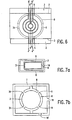
- Fig. 6 is a plan view of another optical element according to the invention, in which switching only takes place within the edge 8.
- the facing parts of the ITO patterns 4, 4', 4", 4'" and 5, 5', 5", 5'" constitute a pattern of a round central part with concentrical rings around it.
- the enveloping edge is not shown in Fig. 6.
- Such an optical element may be used, for example in a diaphragm-operated shutter.
- Fig. 4 shows diagrammatically a CCD camera 20, the front side 21 of which is provided with an optical element as shown in Fig. 1, while a CCD sensor 23 is arranged on the rear side 22.
- incident light 28 is imaged via or not via a lens system on the sensitive part of the CCD sensor 23.
- the camera further comprises a control element 24 (in the form of, for example an IC) which drives the optical element via control wires 26 and drives the sensor 23 via control wires 25, while information is also read from the sensor via the wires 25.
- the assembly is controlled by means of control wires 28, while the information is further read from the sensor via the wires 28.
- Fig. 5a shows a control signal for such a camera.
- the shutter 1 is energized via control wires 26.
- the electrodes 4, 5 of the shutter are energized with a pulse whose pulse height, dependent on the electro-optical material used, is, for example 100 volts at a pulse width t w of 2 msec.
- the shutter is completely blocked and hardly passes incident light 28.
- the charge image which is collected in the image section is (rapidly) transported to the storage section in the CCD sensor 23. Since the optical switch is in its blocked state, incident light 28 will be incident in a fainter form on the image sensor. This fainter light, realized by the optical switch, ensures that the artefact known as smear hardly occurs.
- the pulse 30 drops off, the light is incident on the sensor 23; this particularly applies when a material which is light transmissive (in the unenergized state) such as a gel is chosen. Analogously as for a gel, this also holds for a PDLC, be it that a PDLC is light-diffusing in the unenergized state.
- the shutter is energized again, this time with a pulse 30' of opposite sign.
- the shutter is controlled at such an alternating voltage so as to inhibit degradation of the electro-optical material (LC).
- Fig. 5b shows a variant of the pulse shape of the pulses 30, 30'.
- the pulse shown is formed as a high-frequency AC signal. At a sufficiently high frequency, it is achieved that the electrodes are heated. If necessary, the frequency is adapted, dependent on the ambient temperature and the desired temperature of the shutter.
- Fig. 4 relates to a black-white camera having only one LCD. It will be evident that for color cameras the device is extended in a generally known manner by, for example a prism, color splitters, etc., in which a separate LCD image sensor unit is used for each spectral color.
- the camera of Fig. 4 may also be implemented with an element having a diaphragm function as described with reference to Fig. 6, in which the central part and each concentrical ring can be driven separately.
- the electro-optical element is driven in other applications in such a way that it is partly light- transmissive, preferably with a variable value of the light transmissiveness such as, for example in dipper uses for lamps.
- the electro-optical material then comprises a dye.
- Fig. 7 shows diagrammatically some variants of Fig. 2.
- Fig. 7a shows a variant in which the active area has a rectangular cross-section.
- Such a shutter is used in, for example measuring apparatus for passing or not passing laser beams.
- Fig. 7b shows a variant in which the inlet and outlet apertures 9, 31 are not in line with the filling aperture 18.
- the filling aperture may be present at different positions in the edge 8 at the side of the inlet apertures 9; a possible position for this filling aperture is diagrammatically denoted by the reference numeral 18' in Fig. 7b.
- the active area comprises, for example pixels which can be driven separately.
- one of the two substrates may be opaque when such pixels are reflective (for example in a reflective display for projection purposes).
- the uniform thickness then leads to a capacity which is identical for different switching elements.
- the invention relates to an electro-optical element (shutter) which is switchable between two or more optical states and has a large mechanical rigidity because an extra spacer edge is provided so that no or hardly any spacers are required in the active area.
- an extra spacer edge is provided so that no or hardly any spacers are required in the active area.
Landscapes
- Physics & Mathematics (AREA)
- Nonlinear Science (AREA)
- Mathematical Physics (AREA)
- Chemical & Material Sciences (AREA)
- Crystallography & Structural Chemistry (AREA)
- General Physics & Mathematics (AREA)
- Optics & Photonics (AREA)
- Liquid Crystal (AREA)
Claims (10)
- Optisches Schaltelement (1) mit zwei Substraten (2, 3), die mit einer ersten Ansteuerungselektrode (4) bzw. einer zweiten transparenten Ansteuerungselektrode (5) versehen sind, wobei die genannten Substrate innerhalb eines abschließenden Randes (7) eine Schicht aus einem elektrooptischen Material (6) umschließen, die zwischen mehreren optischen Zuständen umschaltbar ist, dadurch gekennzeichnet, dass sich zwischen den beiden Substraten innerhalb des durch den abschließenden Rand begrenzten Bereichs mindestens ein weiterer Rand (8) befindet, der einen Teil der Schicht des elektrooptischen Materials umgibt und mindestens eine Einlassapertur (9) und mindestens eine Auslassapertur (31) aufweist, wobei der genannten umgebende Rand im Wesentlichen die gleiche Dicke hat wie der abschließende Rand.
- Optisches Schaltelement nach Anspruch 1, dadurch gekennzeichnet, dass der weitere umgebende Rand eine Einlassapertur und eine Auslassapertur hat, die einanander gegenüberliegen.
- Optisches Schaltelement nach Anspruch 1 oder 2, dadurch gekennzeichnet, dass die Einlassapertur und die Auslassapertur in dem umgebenden Rand im Wesentlichen in einer Linie mit einer Füllapertur in dem abschließenden Rand liegen.
- Optisches Schaltelement nach Anspruch 1, 2 oder 3, dadurch gekennzeichnet, dass zum weiteren umgebenden Rand gehörende Teile sich zwischen der Einlassapertur und der Auslassapertur bis an den abschließenden Rand erstrecken.
- Optisches Schaltelement nach einem der vorhergehenden Ansprüche, dadurch gekennzeichnet, dass das Gebiet zwischen dem abschließenden Rand und dem weiteren umgebenden Rand mit Abstandshaltern versehen ist.
- Optisches Schaltelement nach einem der vorhergehenden Ansprüche, dadurch gekennzeichnet, dass das elektrooptische Material zwischen einem lichtdurchlässigen und einem lichtstreuenden Zustand umgeschaltet werden kann.
- Optisches Schaltelement nach einem der Ansprüche 1 bis 6, dadurch gekennzeichnet, dass die erste und die zweite transparente Ansteuerungselektrode mit Ansteuerungsmitteln versehen sind und auf eine derartige Weise strukturiert sind, dass einander gegenüberliegende Teile der transparenten Ansteuerungselektroden im Wesentlichen vollständig durch den weiteren umgebenden Rand begrenzt werden.
- Optisches Schaltelement nach Anspruch 7, dadurch gekennzeichnet, dass die Elektroden innerhalb der durch den weiteren umgebenden Rand begrenzten Teile der Elektroden in Teilelektroden unterteilt sind und die einzelnen Teilelektroden mit einzelnen Ansteuerungsmitteln versehen sind.
- Optisches Schaltelement nach einem der Ansprüche 1 bis 6, dadurch gekennzeichnet, dass in dem weiteren umgebenden Rand und dem abschließenden Rand Abstandshalter vorhanden sind.
- Kamera mit einem ladungsgekoppelten Bauelement (CCD), dadurch gekennzeichnet, dass die Kamera ein optisches Element nach einem der vorhergehenden Ansprüche umfasst sowie Ansteuerungsmittel für das optische Element.
Priority Applications (1)
| Application Number | Priority Date | Filing Date | Title |
|---|---|---|---|
| EP98900114A EP0898729B1 (de) | 1997-02-13 | 1998-01-15 | Optisches schaltelement und kamera mit solchem element |
Applications Claiming Priority (4)
| Application Number | Priority Date | Filing Date | Title |
|---|---|---|---|
| EP97200398 | 1997-02-13 | ||
| EP97200398 | 1997-02-13 | ||
| EP98900114A EP0898729B1 (de) | 1997-02-13 | 1998-01-15 | Optisches schaltelement und kamera mit solchem element |
| PCT/IB1998/000051 WO1998036316A1 (en) | 1997-02-13 | 1998-01-15 | Optical switching element and a camera comprising such an optical element |
Publications (2)
| Publication Number | Publication Date |
|---|---|
| EP0898729A1 EP0898729A1 (de) | 1999-03-03 |
| EP0898729B1 true EP0898729B1 (de) | 2006-03-29 |
Family
ID=26146128
Family Applications (1)
| Application Number | Title | Priority Date | Filing Date |
|---|---|---|---|
| EP98900114A Expired - Lifetime EP0898729B1 (de) | 1997-02-13 | 1998-01-15 | Optisches schaltelement und kamera mit solchem element |
Country Status (2)
| Country | Link |
|---|---|
| EP (1) | EP0898729B1 (de) |
| WO (1) | WO1998036316A1 (de) |
Families Citing this family (1)
| Publication number | Priority date | Publication date | Assignee | Title |
|---|---|---|---|---|
| JP7395368B2 (ja) * | 2020-01-27 | 2023-12-11 | 株式会社ジャパンディスプレイ | 電子機器 |
Family Cites Families (4)
| Publication number | Priority date | Publication date | Assignee | Title |
|---|---|---|---|---|
| FR2364519A1 (fr) * | 1976-09-10 | 1978-04-07 | Thomson Csf | Procede d'assemblage d'une cellule a effet electro-optique, cellule et dispositif d'affichage mis en oeuvre selon le procede |
| DE3049092A1 (de) * | 1980-12-24 | 1982-07-29 | SWF-Spezialfabrik für Autozubehör Gustav Rau GmbH, 7120 Bietigheim-Bissingen | Zelle fuer ein elektrooptisches anzeigeelement und verfahren zu ihrer herstellung |
| JPH0715536B2 (ja) * | 1983-01-28 | 1995-02-22 | キヤノン株式会社 | 表示パネル |
| CH660246A5 (de) * | 1983-07-08 | 1987-03-31 | Bbc Brown Boveri & Cie | Fluessigkristallzelle. |
-
1998
- 1998-01-15 EP EP98900114A patent/EP0898729B1/de not_active Expired - Lifetime
- 1998-01-15 WO PCT/IB1998/000051 patent/WO1998036316A1/en not_active Ceased
Also Published As
| Publication number | Publication date |
|---|---|
| WO1998036316A1 (en) | 1998-08-20 |
| EP0898729A1 (de) | 1999-03-03 |
Similar Documents
| Publication | Publication Date | Title |
|---|---|---|
| US5552841A (en) | Liquid crystal eyeglasses | |
| US5056912A (en) | Projection type image display apparatus | |
| JP4508505B2 (ja) | 液晶表示装置 | |
| JP7315329B2 (ja) | 液晶表示装置及び撮像機能を有する電子機器 | |
| EP0522620A2 (de) | Bildwiedergabenanordnung | |
| CN112987398A (zh) | 显示装置 | |
| KR980010554A (ko) | 액정표시장치 | |
| NL8800595A (nl) | Weergeef- en opneeminrichting voor stereoscopische beeldweergave. | |
| US20090190079A1 (en) | Electro-optic device, electronic instrument, and projection display | |
| EP0625720B1 (de) | Flüssigkristallvorrichtung und methode zu seiner ansteuerung, flüssigkristallgerät und beleuchtungseinrichtung | |
| US4480269A (en) | Television camera | |
| JP2849492B2 (ja) | 投影型液晶表示装置 | |
| CN110488524A (zh) | 显示装置、显示装置中摄像的方法 | |
| EP1574895A1 (de) | Dimmereinirchtung und ansteuerverfahren dafür undabbildungseinrichtung | |
| US6377327B1 (en) | Optical switching element | |
| JP3328496B2 (ja) | 液晶表示装置 | |
| JP2001330844A5 (de) | ||
| JPH1138336A (ja) | 光スイッチング素子 | |
| WO1998036316A1 (en) | Optical switching element and a camera comprising such an optical element | |
| US7492409B2 (en) | Light controller and imaging apparatus | |
| CN113075817A (zh) | 背光模组及液晶显示装置 | |
| JP3826649B2 (ja) | 電気光学装置及び投射型表示装置 | |
| JP4378800B2 (ja) | 表示装置、該表示装置を備えたカメラ | |
| JPH049922A (ja) | 投影型カラー液晶表示装置 | |
| US6347190B1 (en) | Display device of an optical apparatus |
Legal Events
| Date | Code | Title | Description |
|---|---|---|---|
| PUAI | Public reference made under article 153(3) epc to a published international application that has entered the european phase |
Free format text: ORIGINAL CODE: 0009012 |
|
| AK | Designated contracting states |
Kind code of ref document: A1 Designated state(s): DE FR GB NL |
|
| 17P | Request for examination filed |
Effective date: 19990222 |
|
| GRAP | Despatch of communication of intention to grant a patent |
Free format text: ORIGINAL CODE: EPIDOSNIGR1 |
|
| GRAS | Grant fee paid |
Free format text: ORIGINAL CODE: EPIDOSNIGR3 |
|
| GRAA | (expected) grant |
Free format text: ORIGINAL CODE: 0009210 |
|
| AK | Designated contracting states |
Kind code of ref document: B1 Designated state(s): DE FR GB NL |
|
| PG25 | Lapsed in a contracting state [announced via postgrant information from national office to epo] |
Ref country code: NL Free format text: LAPSE BECAUSE OF FAILURE TO SUBMIT A TRANSLATION OF THE DESCRIPTION OR TO PAY THE FEE WITHIN THE PRESCRIBED TIME-LIMIT Effective date: 20060329 |
|
| REG | Reference to a national code |
Ref country code: GB Ref legal event code: FG4D |
|
| REG | Reference to a national code |
Ref country code: GB Ref legal event code: 746 Effective date: 20060331 |
|
| REF | Corresponds to: |
Ref document number: 69834021 Country of ref document: DE Date of ref document: 20060518 Kind code of ref document: P |
|
| NLV1 | Nl: lapsed or annulled due to failure to fulfill the requirements of art. 29p and 29m of the patents act | ||
| ET | Fr: translation filed | ||
| PGFP | Annual fee paid to national office [announced via postgrant information from national office to epo] |
Ref country code: GB Payment date: 20070129 Year of fee payment: 10 |
|
| PGFP | Annual fee paid to national office [announced via postgrant information from national office to epo] |
Ref country code: DE Payment date: 20070312 Year of fee payment: 10 |
|
| PLBE | No opposition filed within time limit |
Free format text: ORIGINAL CODE: 0009261 |
|
| STAA | Information on the status of an ep patent application or granted ep patent |
Free format text: STATUS: NO OPPOSITION FILED WITHIN TIME LIMIT |
|
| 26N | No opposition filed |
Effective date: 20070102 |
|
| PGFP | Annual fee paid to national office [announced via postgrant information from national office to epo] |
Ref country code: FR Payment date: 20070129 Year of fee payment: 10 |
|
| GBPC | Gb: european patent ceased through non-payment of renewal fee |
Effective date: 20080115 |
|
| PG25 | Lapsed in a contracting state [announced via postgrant information from national office to epo] |
Ref country code: DE Free format text: LAPSE BECAUSE OF NON-PAYMENT OF DUE FEES Effective date: 20080801 |
|
| REG | Reference to a national code |
Ref country code: FR Ref legal event code: ST Effective date: 20081029 |
|
| PG25 | Lapsed in a contracting state [announced via postgrant information from national office to epo] |
Ref country code: GB Free format text: LAPSE BECAUSE OF NON-PAYMENT OF DUE FEES Effective date: 20080115 |
|
| PG25 | Lapsed in a contracting state [announced via postgrant information from national office to epo] |
Ref country code: FR Free format text: LAPSE BECAUSE OF NON-PAYMENT OF DUE FEES Effective date: 20080131 |