EP0896426A1 - Verfahren zum Simulieren einer nichtlinearen Verstärkers mit Hüllkurvenspeicher - Google Patents
Verfahren zum Simulieren einer nichtlinearen Verstärkers mit Hüllkurvenspeicher Download PDFInfo
- Publication number
- EP0896426A1 EP0896426A1 EP98401958A EP98401958A EP0896426A1 EP 0896426 A1 EP0896426 A1 EP 0896426A1 EP 98401958 A EP98401958 A EP 98401958A EP 98401958 A EP98401958 A EP 98401958A EP 0896426 A1 EP0896426 A1 EP 0896426A1
- Authority
- EP
- European Patent Office
- Prior art keywords
- amplitude
- frequency
- signal
- components
- input
- Prior art date
- Legal status (The legal status is an assumption and is not a legal conclusion. Google has not performed a legal analysis and makes no representation as to the accuracy of the status listed.)
- Withdrawn
Links
Images


Classifications
-
- H—ELECTRICITY
- H03—ELECTRONIC CIRCUITRY
- H03F—AMPLIFIERS
- H03F1/00—Details of amplifiers with only discharge tubes, only semiconductor devices or only unspecified devices as amplifying elements
- H03F1/32—Modifications of amplifiers to reduce non-linear distortion
- H03F1/3241—Modifications of amplifiers to reduce non-linear distortion using predistortion circuits
Definitions
- the present invention relates to the field of response simulation in signal from non-linear amplifiers and relates to a signal simulation system response of a non-linear amplifier with a memory effect.
- An application of such a system is the simulation of amplification high efficiency microwave, in particular in class AB, B or C of amplification and more particularly the simulation of response of power amplifiers in the state solid, SSPA type, and amplifiers based on wave tubes progressive, TOP or TWT type, used in transmission links by terrestrial or satellite radio beam.
- Such amplifying devices exhibit a non-linear response characteristic.
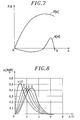
- Figure 1 illustrates an example of an input-output response curve ANL non-linear amplifier.
- the curve giving the output signal level g of the amplifier ANL as a function of the input signal level x is typically bent at high amplitudes A of the input signal x, due to phenomena of saturation.
- gain is not constant depending on the input signal level x, we speak of amplifier operating in a non-linear regime or more simply in non-linear amplification.
- Amplifiers without memory exhibit strong non-linearity in amplitude and less phase distortion.
- the response characteristic input / output of an amplifier without ANL memory can then be reduced, as illustrated in figure 1, with a single curve g (x).
- a (t) represents the envelope of the input signal, which is defined by the limits in amplitude in which the sinusoidal signal x evolves, the envelope varying according to the time.
- FIG. 3 illustrates a timing diagram of a signal x (t) having an envelope A constant.
- g (t) C (A (t)). cos (2 ⁇ .f 0 .t + ⁇ (t))
- C (A) is the Chebyshev transform of the input / output response curve g (x).
- the response of a non-linear ANL amplifier without memory to a signal x modulated can therefore be modeled and simulated simply by a single curve C (A), an example of which is illustrated in solid lines in FIG. 6A.
- A Such a curve giving the output amplitude C as a function of the input amplitude A is called the amplitude non-linearity and noted abbreviated AM / AM curve.
- Figure 2 illustrates a response characteristic of a non-linear amplifier with memory ANLAM, on which a phenomenon of hysteresis appears caused by memory effect.
- the rise curves m and m ' hysteresis do not overlap when the respective amplitudes A and A 'of the signal input x are different.
- the variation in the memorization time linked to the variation amplitude prevents the curves m and m 'from overlapping.
- Figure 7 illustrates an example of curves P (A) and Q (A) equivalent to curves C (A) and ⁇ (A) of Figures 6A and 6B.
- the known quasi-memoryless amplifier response simulation models generally prefer to use features as a pair of curves P (A) and Q (A) rather than as a pair of curves C (A) and ⁇ (A), well that these pairs of curves are strictly equivalent.
- a known principle of non-linear amplifier simulation consists in precharacterize the amplifier produced on a test bench, precharacterization being performed with a signal of determined frequency and amplitude, in order to simulate then the response to a signal of any frequency and amplitude.
- a single frequency signal f 0 taking different amplitudes A ', A'', A ′′′ is applied to the amplifier tested to obtain its characteristics, illustrated for example in FIG. 6 or 7.
- HB Poza's simulator stores only a pair of AM / AM and AM / PM curves, for example the pair of curves obtained at the frequency f 0 , and reconstructs the other pairs of curves (not stored) corresponding to the other frequencies f 0 - , f 0 + or at intermediate frequencies.
- An unstored curve is deduced simply by translating the stored curve of a suitable vector.
- the simulator calculates the components along the axis (A) and along the axis (C) or ( ⁇ ) of the translation vector to best approximate the frequency curve f 0 , shown in solid line in FIG. 6A or 6B, of the frequency curve f 0 - or f 0 + , shown in dotted lines.
- Another disadvantage of such a system is that it does not simulate the response from a memory amplifier.
- FIG. 9 illustrates another known system of simulation, according to the model of A.A.M. Saleh, described in an article titled “Frequency-independent and frequency-dependent models of TWTA Amplifiers "published in November 1981 in the review” IEEE transactions on communication ", volume com-29, n ° 11, page 1715.
- the calculation of the response to an input signal x from a quasi-memoryless non-linear amplifier is decomposed into two stages P (A, f) and Q (A, f) of calculation of two components yp and yq respective of the output signal y.
- the yp component is in phase with the signal input x, while the component yq is in phase quadrature.
- Saleh's simulation system uses characterization results from the amplifier at several frequencies f, several pairs of curves P (A) and Q (A) being established at several frequencies f to calculate transfer functions P (A, f) and Q (A, f) corresponding to each branch of calculation of the components yp and yq of the signal output y.
- Each of the transfer functions P (A, f) or Q (A, f) corresponds to the calculation of a non-linear response without memory effect, no phase shift being introduced in each of these calculation branches.
- Another disadvantage of this model is that it does not apply to memory amplifiers, the system not accounting for distortions appearing at different frequencies when the signal amplitude changes rapidly compared to the storage time constants.
- FIG. 10 illustrates the simulation system described by MT Abuelma'atti which as before comprises two branches for calculating the components in phase yp and in quadrature yq of the output signal y, each branch calculating the contribution of a series of N functions of Bessel J1 depending on the amplitude A of the input signal x, by weighting each function J1 by a coefficient ⁇ and a factor G (f) of frequency correction.
- the coefficients ⁇ n and the factors G n (f) are calculated after having established several pairs of curves P (A) and Q (A) characteristic of the non-linear amplifier, the curves being established at several test frequencies f the amplifier.
- Bessel functions are the Chebychev transforms of sinusoidal functions and that the development following Bessel functions of curves P (A) and Q (A) corresponds to a Fourier expansion following sinusoidal functions of the amplifier's non-linearity curves y (x), which elegantly suited to the sinusoidal shape of the hysteresis curves y (x), such as illustrated in figure 2.
- such a system should allow the simulation of amplification of multi-carrier signals, i.e. signals comprising several sinusoidal components of distinct frequencies.
- Figures 11-14 illustrate the appearance of the intermodulation phenomenon during non-linear amplification of a two-carrier signal.
- FIG. 11 represents a frequency diagram of input signal x two-carrier, on which we see for example, two carrier components of respective frequencies f -1 and f 1 having an equal amplitude A input.
- the two carrier frequencies f -1 and f 1 located in the useful band BU of the amplifier frequency, are separated by a frequency difference df.
- FIG. 14 represents a frequency diagram of output signal y which corresponds to ANLAM amplification with memory effect of the input signal x two-carrier in Figure 11.
- the output signal has a series of harmonics of various frequencies f and of different amplitudes C.
- the frequency of each of the intermodulation components is a integer combination of input carrier frequencies.
- Figure 15 reproduces results provided by the Abuelma'atti model which allowed an estimation of the amplitudes C -1 , C 1 , and C -3 , C 3 of output of the carrier components and the order intermodulation components 3.
- the estimation of the amplitude of the intermodulation components by the Abuelma'atti's model does not correspond well to the reality of distortion measurements intermodulation when amplifying multi-carrier microwave signals by a memory amplifier in non-linear operation with high efficiency.
- envelope memory when amplifying a multi-carrier signal.
- envelope memory when amplifying a multi-carrier signal, the envelope, defined by the positive and negative limits in amplitude of the signal, is not constant.
- FIG. 12 which illustrates the temporal evolution of the input signal x two-carrier of FIG. 11, shows for example that the envelope X (t) and -X (t) of the two-carrier signal varies very quickly and in significant proportions, whereas the amplitude A of each carrier f 1 and f -1 carrier is assumed to be constant.
- FIG. 13 which illustrates the temporal evolution of the output signal y corresponding to the previous input signal x two-carrier, thus shows that the envelope Y (t) and -Y (t) of the output signal y, then appears very distorted by the distortions intermodulation. These are referred to as the envelope memory effect. amplitude distortions of the signal by a non-linear amplifier with memory.
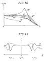
- the first effect observed is that the C1 / C3 ratio illustrated in Figure 16, comparing the amplitude C1 of carriers with respect to the amplitude C3 of the components intermodulation, varies considerably according to the frequency difference df of the carriers and according to the precise value of the amplitude A of the carriers of the input signal.
- the second effect observed is that the presence of a second carrier influences the output amplitude of the first carrier.
- FIG. 17 shows for example peaks of weakening or resonance of amplitude C1 or C-1 of output of each of the carriers of frequency f 1 or f -1 , according to the frequency difference df of the two carriers (df being equal to f 1 -f -1 ).
- the object of the invention is to provide a response simulation system by signal from a non-linear amplifier having a memory effect without them aforementioned drawbacks.
- a primary object of the invention is to obtain precise simulations of the effects of envelope memory on non-linear amplifiers.
- a particular object of the invention is to obtain precise simulations of amplification of multi-carrier signals by a non-linear memory amplifier.
- Another object of the invention is to provide a simple system for simulating response from non-linear memory amplifiers.
- the invention provides a measure dynamic characteristics of the amplifier under the conditions where distortions, that is to say with an amplitude modulated signal, which makes it possible to vary the signal envelope.
- the amplitude modulation distortions each measurement being made by modulating the input amplitude.
- These measurements of modulation distortion characteristics allow to calculate modulation transfer functions reproducing at output the amplitudes of the distortions according to the amplitudes of modulation at input.
- the amplitudes of distortions reproduced by the transfer functions modulation correct the output of direct transfer functions from a known model.
- the known models were obtained by measuring characteristics of amplitude / amplitude conversion and amplitude / phase shift conversion of the amplifier, each measurement being carried out at constant amplitude at the input, then at developing the characteristics as a result of direct transfer function.
- Modulation distortion characteristic measurements are performed more precisely with multi-carrier signals, that is to say by applying signals comprising several frequency components (carriers) at input of the non-linear amplifier, the amplified signals at the output presenting a multitude of frequency components (amplified carriers + intermodulation products).
- the amplifier has a variation in carrier gain in depending on the envelope frequency, it is planned to measure characteristics of amplitude gain for a carrier in the presence of another carrier as a function of the carrier differential.
- the means for generating harmonics of the device include preferably according to the invention a Fourier decomposition module of a signal into frequency components and / or a combinatorial module calculating the combinations frequency of intermodulation components and / or a normative module calculating an effective signal amplitude value.
- a first embodiment of the device according to the invention provides that the modulation filter has a transfer function established from characteristics of rejection of intermodulation components, so that components amplitude intermodulation calculated by the modulation filter are added to the response of the calculation module when the amplification of a multi-carrier signal is simulated by the device.
- a second embodiment of the device according to the invention provides in in addition to a filter for correcting the response of the calculation module, the filter having a transfer function established from interaction characteristics of carriers, so that the amplitude of a carrier provided by the calculation module is corrected by the correction filter when the amplification of a multi-carrier signal is simulated by the device.
- the invention advantageously applies to the simulation of response in signal from a high efficiency microwave amplifier.
- the simulation methods and device according to the invention are developed at from known models.
- the invention proposes to simulate the amplification of shape signals any and especially of signals comprising several components frequency.
- the device simulation includes means for generating harmonics in response to a multi-carrier signal.
- FIGS. 21 to 23 systematically include a block 11 or 21 or 31 for signal calculation output y according to a known model and a parallel block 12 or 22, 23 or 32 of generation of harmonics which calculates the frequencies of the components intermodulation before calculating their precise amplitude to correct the signal exit there.
- the output signal calculation blocks 11, 21 and 31 are provided for putting implement a known simulation model, for example and respectively the model non-linear without memory MNLSM by H.B. Poza, the non-linear model without Quadratic MNLSM memory of A.A.M. Saleh and the MM memory model of M.T. Abuelma'atti.
- Other models can be implemented, and the description of the implementation of the invention will be developed mainly from the model perfected by M.T. Abuelma'atti.
- the parallel structure of the MNLSM output calculation blocks or MM and Harm blocks for generating harmonics is indicative, the structure of blocks being able to be in series, and the effective realization of the blocks of calculations being of preferably done by computer programs, the blocks schematically in this case the functions of calculation subroutines.
- FIG. 23 describes the detail of an alternative embodiment of Harm means for generating harmonics and MM means for calculating the intermodulation components perfected from the simple Abuelma'atti model illustrated in FIG. 10.
- the Harm and MM modules allow the calculation of the amplitudes of intermodulation components ..., Y 010 , Y 1-11 , Y -120 , Y -111 , Y 0-12 , Y -102 , Y 20-1 , Y 2- 10 , Y 11-1 , Y 02-1 , ... when the input signal x comprises a multitude of frequency components A, B, ..., M.
- This complex embodiment of means Harm and MM is intended for the simulation of the amplification of signals of any shape, in particular of multi-carrier signals.
- Harm means for generating harmonics include an FFT filter for decomposition in Fourier series to decompose the multifrequency input signal x into frequency components of amplitude A, B, ..., M. These components are applied as input to elementary filters grouped by tables corresponding to the calculation of an intermodulation component, for example Y 010 .
- Each elementary filter has a transfer function resulting from a generalized Bessel function J on the example of the filters of FIG. 10. The formulas of the transfer functions of the filters of the table and of the generalized Bessel functions will be detailed in the developments below. -after.
- the architecture of a device according to the invention comprises means for generating harmonics, preferably with a decomposition module in Fourier series and a known simulation model.
- the envelope Y of the output signal corresponding to the bi-carrier input signal x of equations 9 and 10 comprises a series of frequency components denoted f i and amplitude denoted C i , i being a positive or negative integer.
- the order of the intermodulation components is the sum of the absolute values of the integer coefficients of combination of the carrier frequencies.
- the order 0, 1, 2 or N of a Bessel function J0, J1, J2 or JN is chosen so as to correspond to the absolute value of the integer coefficient of combination of a carrier frequency f -1 or f 1 in the frequency f i of the intermodulation component of amplitude C i .
- of each intermodulation component C i therefore corresponds to the sum of the orders 0, 1, 2 or N of the Bessel functions J0, J1, J2 or JN involved in each formula.
- n is the Bessel function of the first type and of absolute value order of n (generalization).
- FIG. 20 thus illustrates a sophisticated embodiment of MM calculation means of intermodulation components developed from these model formulas to memory.
- a determining quality factor in the design and choice of a microwave amplification system is the ratio of the amplitude C 3 of the strongest intermodulation component at output and of the amplitude C 1 at output of a carrier component.
- the rejection factor is generally expressed in power, which corresponds to the following ratio: C1 2 / C3 2 noted here P / I 2 .
- the frequency correctors G n (f i ) have a weak correction effect, the curve of the correctors G n being calculated from measurements with a single carrier, therefore without modulation of the input envelope.
- the intermodulation rejection factors P / I thus calculated do not depend on the frequency difference df of the carriers, unlike the resonance effects observed and illustrated for example in FIG. 16.
- the signal y (t) calculated according to the model of Abuelma'atti is compared to a signal z (t) comprising components intermodulation as actually measured. Such a comparison provides the value of a modulation signal u (t) which will be simulated by a modulation filter according to the invention.
- Figure 21 shows schematically a first embodiment of the device according to the invention, which includes such a modulation filter 14.
- the filter 14 has a function of transfer E (f, H) which calculates the signal u according to the input signal.
- the y signal of known model 11 is then corrected by the modulator signal u to provide a signal z which reproduces the modulation distortions actually measured.
- the modulator signal u is useful only if the signal input has an amplitude modulated envelope X. Indeed, when the input signal x is not modulated, the known model 11 has an output signal y which simulates the amplifier's response appropriately.
- the invention specifically provides for obtaining the signal envelope by taking the square of the signal standard x.
- FIG. 21 thus shows that the filter 14 receives as input the effective value X 2 (t) of the envelope of the input signal x.
- the signal z simulated according to the invention has an envelope Z which corresponds to the envelope Y of the output signal y simulated by the known model MNLSM or MM, and the modulator signal u is advantageously zero.
- E (0, A) has a zero value, since it is useless to have a modulator signal u when there is no carrier frequency difference.
- K A 2 .E (df, A)
- Equation (12) Equivalently to equation (12), we prefer here to write the envelope Y of the output signal y of the known model in the following complex and exponential form: where i is an odd integer taking all negative and positive values.
- Is : Y (t) ... + C -5 .exp (-j.5 ⁇ .df.t) + C -3 .exp (-j.3 ⁇ .df.t) + C -1 .exp (-j. ⁇ .df.t) + C 1. exp (j. ⁇ .df.t) + C 3 .exp (j.3 ⁇ .df.t) + C 5 .exp (j.5 ⁇ .df.t) + ...
- the first embodiment it is sought to modulate only the amplitude of the intermodulation components of order 3 by modifying at least the amplitude of the carrier components (order 1) calculated by the known model. This is achieved by minimizing the value of K, so that the terms KC -3 , KC 1 , KC -1 and KC 3 are negligible.
- the two central lines of equation (25) indicate that the carrier components of frequency f -1 and f 1 do indeed have an amplitude substantially equal to C -1 and C 1 , respectively, in the output signal z module.
- K
- FIG. 18 provides a diagram of the system of measurements carried out according to the invention.
- the continuity of the transfer function E (df, H) according to the amplitude H of the harmonics h at input or according to the power X 2 of the envelope of the input signal x is obtained by interpolating the discrete values from the table of values unknown K.
- the unknown values K can also be interpolated between the chosen values df ', df ", df ′′′, df" "of frequency difference df.
- a computer program preferably performs such calculations and stores the values of unknown K in the form of a matrix.
- the frequency asymmetries of the amplifier response can then be simulated by this variant of the first embodiment.
- the invention provides that the transfer function E '(df, H) of the filter 14 can be asymmetrical.
- C i the modulated components of the modulated output signal z' obtained according to this variant of the first embodiment.
- the output signal z ' is also obtained by modulating the signal y of a known model by a modulator signal u' calculated by the transfer function E 'of the filter 34 of FIG. 23. This makes it possible to distinguish the components C' i modulated according to the invention, components C i calculated by the model with no known MNLSM memory.
- the amplifier has an asymmetrical response around the carrier frequencies, it is provided according to the invention to measure intermodulation rejection characteristics, by providing for measuring the two rejection factors P / I + higher and P / I - lower for each amplitude A and frequency difference df of carriers, in order to simulate the distortions of modulation at output.
- a second embodiment of the invention makes it possible to simulate the second effect intermodulation distortion.
- the second effect observed is the variation of the gain of the carriers as a function of the envelope frequency df / 2, illustrated for example in FIG. 17.
- the invention provides for adjusting the amplitudes C 1 and C -1 of the carrier output calculated by a known model, taking into account measurements of characteristics C1 / C-1 of carrier interaction.
- the adjustment of the second embodiment is combined with the adjustment of the main intermodulation components C 3 and C- 3 provided for in the first embodiment of the invention, described above. It is also possible to provide for an adjustment of the secondary intermodulation components C 5 and C 5 .
- the adjustment is performed by correcting the output signal y, or preferably the modulated signal z or z ', by a correction signal v coming from a filter 37 having a transfer function F of correction.
- F is the correction transfer function expressed as a function of the envelope modulation frequency, i.e. the frequency difference df of amplitude A carriers at input.
- Equations 35 to 38 form a system of four equations with four unknowns K + , K - , L + , L - which is solved in a known manner.
- the resolution of the last two equations 37 and 38 provides the values of the correction unknowns L + and L - .
- Such complete measurements of amplitudes of components at the output of a amplifier comprising both component rejection measurements intermodulation of order 3 and 5 at output and carrier interaction measurements thus allow to fully simulate the signal response with distortions due to the envelope memory effect of a non-linear amplifier with memory.
- partial measures such as rejection measures C1 / C3 3 order intermodulation or C1 / C-1 carrier interaction measurements are sufficient to characterize certain intermodulation distortion effects.
- a second embodiment allows validation of the model by measurement signal-to-noise ratio in the presence of a high number of carriers whose density DSP power spectral is modeled by white noise.
- FIGS. 19A and 19B thus illustrate a frequency diagram of noise, respectively applied at the input and measured at the output of a non-linear amplifier memory to characterize it.
- white noise is applied having a DSP power spectral density of constant NP level in a band of frequency BW except in a window BH of frequency in which the noise is absent.
- This input signal although having a constant spectral density is of amplitude variable. It therefore makes it possible to measure the modulation distortions appearing in amplifier output. The distortions appear at the amplifier output under form of noise transfer in the previously defined BH window.
- the characterization of the amplifier consists in measuring its capacity to limit the noise transfer in the BH window by measuring the difference in noise level NPR as output, in the BW frequency band and in the BH window.
- a third mode of checking the validity of the model consists in measuring the bit error rate during amplification of modulated carriers.
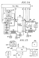
- FIG. 24 illustrates a test bench used to establish, according to the invention, non-linear DUT amplifier characteristic measurements with memory.
- This bench of test whose understanding of the operation is within the reach of the skilled person, in particular comprises an amplitude modulated signal generation block 10 with, for example, two generators SG1 and SG2 of frequencies which can be distinct for apply a multi-carrier signal to the DUT amplifier device to be characterized.
- he further includes a noise measurement block 20 with an NG noise generator white with window and possibly a block 30 for measuring the bit error rate with a MOD generator of signals modulated by a random binary message and a comparator Comp of the original signal and the amplifier return signal.
- FIG. 25 finally illustrates a diagram of the characteristics files set up work by a computer program to simulate the non-linear amplification according to the method of the invention.
- the Pro program thus calls up a file 203 storing results of measurements of static AP characteristics, i.e. of C, ⁇ curves or curves P, Q established at constant amplitude (in a known manner).
- the Pro program still uses a series of files 205, 206, 207 storing dynamic P / I characteristic measurement results as intermodulation rejection curves C1 / C3 or interaction interaction curves C1 / C-1 carriers.
- Each file 205 or 206 or 207 of the series is established for example for a frequency difference df of carriers.
- the program is launched after having entered general data on the amplifier to simulate.
- the Pro program provides a file 204 of the coefficients ⁇ in succession direct transfer functions, in particular Bessel functions. It mainly provides according to the invention files 208, 209 containing the data of the transfer functions E modulation and F correction above.
- Figure 26 shows an example of process step diagram implemented works through such a Pro program.
- the device according to the invention is preferably produced under form of computer program whose functions correspond to blocks shown schematically by way of example in FIGS. 20 to 24.
Applications Claiming Priority (2)
| Application Number | Priority Date | Filing Date | Title |
|---|---|---|---|
| FR9710052 | 1997-08-01 | ||
| FR9710052A FR2766992B1 (fr) | 1997-08-01 | 1997-08-01 | Procede de simulation d'amplificateur non lineaire a memoire d'enveloppe |
Publications (1)
| Publication Number | Publication Date |
|---|---|
| EP0896426A1 true EP0896426A1 (de) | 1999-02-10 |
Family
ID=9510071
Family Applications (1)
| Application Number | Title | Priority Date | Filing Date |
|---|---|---|---|
| EP98401958A Withdrawn EP0896426A1 (de) | 1997-08-01 | 1998-07-30 | Verfahren zum Simulieren einer nichtlinearen Verstärkers mit Hüllkurvenspeicher |
Country Status (4)
| Country | Link |
|---|---|
| US (1) | US6216100B1 (de) |
| EP (1) | EP0896426A1 (de) |
| JP (1) | JPH11191716A (de) |
| FR (1) | FR2766992B1 (de) |
Cited By (1)
| Publication number | Priority date | Publication date | Assignee | Title |
|---|---|---|---|---|
| WO2001003287A1 (en) * | 1999-06-30 | 2001-01-11 | Wireless Systems International Limited | Reducing distortion of signals |
Families Citing this family (13)
| Publication number | Priority date | Publication date | Assignee | Title |
|---|---|---|---|---|
| US6801086B1 (en) * | 2002-04-03 | 2004-10-05 | Andrew Corporation | Adaptive digital pre-distortion using amplifier model that incorporates frequency-dependent non-linearities |
| JP4394409B2 (ja) * | 2003-09-25 | 2010-01-06 | 株式会社日立国際電気 | プリディストーション方式歪補償機能付き増幅器 |
| US7071777B2 (en) * | 2003-12-02 | 2006-07-04 | Motorola, Inc. | Digital memory-based predistortion technique |
| US20060039498A1 (en) * | 2004-08-19 | 2006-02-23 | De Figueiredo Rui J P | Pre-distorter for orthogonal frequency division multiplexing systems and method of operating the same |
| US7856483B2 (en) | 2004-12-10 | 2010-12-21 | Microsoft Corporation | Information management systems with time zone information, including event scheduling processes |
| CN1983851B (zh) * | 2006-06-16 | 2010-07-28 | 华为技术有限公司 | 一种使功放支持多功率的方法及射频模块 |
| EP1968205A1 (de) * | 2007-02-28 | 2008-09-10 | Nederlandse Organisatie voor toegepast- natuurwetenschappelijk onderzoek TNO | Bestimmung der Signalqualität in Kabelnetzwerken |
| JP4918572B2 (ja) * | 2009-07-02 | 2012-04-18 | 株式会社日立国際電気 | プリディストーション方式歪補償機能付き増幅器 |
| JP5903758B2 (ja) | 2010-09-08 | 2016-04-13 | ソニー株式会社 | 信号処理装置および方法、プログラム、並びにデータ記録媒体 |
| US9577855B1 (en) | 2011-07-13 | 2017-02-21 | Softronics, Ltd. | Channelized multicarrier digitizer |
| FR2999364A1 (fr) * | 2012-12-10 | 2014-06-13 | Centre Nat Etd Spatiales | Procede d'evaluation predictive de la puissance d'intermodulation dans un dispositif electronique |
| US20150160279A1 (en) * | 2013-12-09 | 2015-06-11 | Qualcomm Incorporated | Quantitative characterization of nonlinearity and memory effect in nonlinear circuits |
| US20170024495A1 (en) * | 2015-07-21 | 2017-01-26 | Positive Grid LLC | Method of modeling characteristics of a musical instrument |
Citations (1)
| Publication number | Priority date | Publication date | Assignee | Title |
|---|---|---|---|---|
| US5579342A (en) * | 1994-09-22 | 1996-11-26 | Her Majesty The Queen In Right Of Canada As Represented By The Minister Of Communications | Pre-compensated frequency modulation (PFM) |
-
1997
- 1997-08-01 FR FR9710052A patent/FR2766992B1/fr not_active Expired - Fee Related
-
1998
- 1998-07-29 US US09/124,430 patent/US6216100B1/en not_active Expired - Fee Related
- 1998-07-30 EP EP98401958A patent/EP0896426A1/de not_active Withdrawn
- 1998-08-03 JP JP10251762A patent/JPH11191716A/ja not_active Abandoned
Patent Citations (1)
| Publication number | Priority date | Publication date | Assignee | Title |
|---|---|---|---|---|
| US5579342A (en) * | 1994-09-22 | 1996-11-26 | Her Majesty The Queen In Right Of Canada As Represented By The Minister Of Communications | Pre-compensated frequency modulation (PFM) |
Non-Patent Citations (4)
| Title |
|---|
| BOSCH W ET AL: "MEASUREMENT AND SIMULATION OF MEMORY EFFECTS IN PREDISTORTION LINEARIZERS", IEEE TRANSACTIONS ON MICROWAVE THEORY AND TECHNIQUES, vol. 37, no. 12, 1 December 1989 (1989-12-01), pages 1885 - 1890, XP000173168 * |
| CARDINAL J -S ET AL: "A NEW ADAPTIVE DOUBLE ENVELOPE FEEDBACK (ADEF) LINEARIZER FOR SOLIDSTATE POWER AMPLIFIERS", IEEE TRANSACTIONS ON MICROWAVE THEORY AND TECHNIQUES, vol. 43, no. 7, PART 01, 1 July 1995 (1995-07-01), pages 1508 - 1515, XP000514134 * |
| GHADERI M ET AL: "FAST ADAPTIVE POLYNOMIAL I AND Q PREDISTORTER WITH GLOBAL OPTIMISATION", IEE PROCEEDINGS: COMMUNICATIONS, vol. 143, no. 2, 1 April 1996 (1996-04-01), pages 78 - 86, XP000592638 * |
| KARAM G ET AL: "IMPROVED DATA PREDISTORTION USING INTERSYMBOL INTERPOLATION", WORLD PROSPERITY THROUGH COMMUNICATIONS, BOSTON, JUNE 11 - 14, 1989, vol. VOL. 1, no. -, 11 June 1989 (1989-06-11), INSTITUTE OF ELECTRICAL AND ELECTRONICS ENGINEERS, pages 286 - 291, XP000075470 * |
Cited By (2)
| Publication number | Priority date | Publication date | Assignee | Title |
|---|---|---|---|---|
| WO2001003287A1 (en) * | 1999-06-30 | 2001-01-11 | Wireless Systems International Limited | Reducing distortion of signals |
| US7106806B1 (en) | 1999-06-30 | 2006-09-12 | Andrew Corporation | Reducing distortion of signals |
Also Published As
| Publication number | Publication date |
|---|---|
| US6216100B1 (en) | 2001-04-10 |
| JPH11191716A (ja) | 1999-07-13 |
| FR2766992A1 (fr) | 1999-02-05 |
| FR2766992B1 (fr) | 2000-12-29 |
Similar Documents
| Publication | Publication Date | Title |
|---|---|---|
| EP0896426A1 (de) | Verfahren zum Simulieren einer nichtlinearen Verstärkers mit Hüllkurvenspeicher | |
| EP0797294A1 (de) | Korrekturverfahren für nichtlineare Verzerrungen in einem Verstärker und Radiosender damit | |
| FR2494059A1 (fr) | Procede et dispositif de demodulation de porteuse a acquisition rapide | |
| EP2341614B1 (de) | Linearisierungsvorrichtung für Leistungsverstärker | |
| Sombrin | On the formal identity of EVM and NPR measurement methods: Conditions for identity of error vector magnitude and noise power ratio | |
| EP0073869B1 (de) | Einrichtung zum Datenempfang mit einem hörerseitigen Echokompensator | |
| WO2019207476A1 (fr) | Systeme et procede de linearisation en bande de base pour un amplificateur de puissance radiofrequence de classe g | |
| EP3835811B1 (de) | Verfahren zur entkopplung von signalen in sende-/empfangssystemen | |
| WO2017186861A1 (fr) | Procede et dispositif de reduction de bruit dans un signal module | |
| WO2020074428A1 (fr) | Systeme d'emission multi-voies auto calibre pour charge utile de satellite | |
| EP0121446B1 (de) | Schaltung zur Linearisierung eines Hochfrequenzverstärkers mit nichtlinearen komplexen Koeffizienten | |
| US20220065972A1 (en) | Fast Convergence Method for Cross-Correlation Based Modulation Quality Measurements | |
| FR2717294A1 (fr) | Procédé et dispositif de synthèse dynamique sonore musicale et vocale par distorsion non linéaire et modulation d'amplitude. | |
| CA2218925A1 (fr) | Estimateur d'un defaut de fonctionnement d'un modulateur en quadrature et etage de modulation l'utilisant | |
| FR2595895A1 (fr) | Double demodulateur numerique | |
| EP2114045B1 (de) | Behebung der unvollkommenheiten eines demodulators | |
| FR3003114A1 (fr) | Procede et systeme de test d'un appareil audio | |
| WO1991012697A1 (fr) | Procede, et dispositif, de mesure unique pour visualiser et qualifier la linearite d'une chaine de transmission | |
| EP2028810A1 (de) | Korrektur von Verzerrungen in einem Sender | |
| FR2540309A1 (fr) | Dispositif de linearisation d'un amplificateur haute frequence a non-linearite d'amplitude | |
| CN112436906B (zh) | 无线调制信号调制质量参数校准设备 | |
| JPWO2004004264A1 (ja) | 検波器、試験装置、試験方法、及びプログラム | |
| FR3135847A1 (fr) | Procédé de pré-distorsion d’un signal d’entrée pour compenser l’effet d’une fonction de transfert non-linéaire d’un amplificateur de puissance, produits programme d’ordinateur et dispositifs correspondants. | |
| JP2023043167A (ja) | 等価非線形雑音の生成方法及び装置 | |
| Wen et al. | Modeling and compensation of a non-ideal I/Q-modulator |
Legal Events
| Date | Code | Title | Description |
|---|---|---|---|
| PUAI | Public reference made under article 153(3) epc to a published international application that has entered the european phase |
Free format text: ORIGINAL CODE: 0009012 |
|
| AK | Designated contracting states |
Kind code of ref document: A1 Designated state(s): DE FR GB IT |
|
| AX | Request for extension of the european patent |
Free format text: AL;LT;LV;MK;RO;SI |
|
| 17P | Request for examination filed |
Effective date: 19990722 |
|
| AKX | Designation fees paid |
Free format text: DE FR GB IT |
|
| GRAP | Despatch of communication of intention to grant a patent |
Free format text: ORIGINAL CODE: EPIDOSNIGR1 |
|
| RAP1 | Party data changed (applicant data changed or rights of an application transferred) |
Owner name: FRANCE TELECOM S.A. |
|
| STAA | Information on the status of an ep patent application or granted ep patent |
Free format text: STATUS: THE APPLICATION IS DEEMED TO BE WITHDRAWN |
|
| 18D | Application deemed to be withdrawn |
Effective date: 20080110 |