EP0887675A2 - Gegenstand bestehend aus einer an einer mikromechanischen Vorrichtung befestigten optischen Faser - Google Patents
Gegenstand bestehend aus einer an einer mikromechanischen Vorrichtung befestigten optischen Faser Download PDFInfo
- Publication number
- EP0887675A2 EP0887675A2 EP98304774A EP98304774A EP0887675A2 EP 0887675 A2 EP0887675 A2 EP 0887675A2 EP 98304774 A EP98304774 A EP 98304774A EP 98304774 A EP98304774 A EP 98304774A EP 0887675 A2 EP0887675 A2 EP 0887675A2
- Authority
- EP
- European Patent Office
- Prior art keywords
- layer
- movable
- micro
- pressure
- article
- Prior art date
- Legal status (The legal status is an assumption and is not a legal conclusion. Google has not performed a legal analysis and makes no representation as to the accuracy of the status listed.)
- Ceased
Links
- 239000013307 optical fiber Substances 0.000 title claims abstract description 30
- 230000003287 optical effect Effects 0.000 claims abstract description 88
- 238000002310 reflectometry Methods 0.000 claims abstract description 48
- 239000011521 glass Substances 0.000 claims description 14
- 239000012530 fluid Substances 0.000 claims description 9
- 238000004891 communication Methods 0.000 claims description 8
- 238000013016 damping Methods 0.000 claims description 6
- 239000000853 adhesive Substances 0.000 claims description 4
- 230000001070 adhesive effect Effects 0.000 claims description 4
- 239000008280 blood Substances 0.000 claims 1
- 210000004369 blood Anatomy 0.000 claims 1
- 230000004044 response Effects 0.000 abstract description 34
- 239000012528 membrane Substances 0.000 abstract description 11
- 238000009530 blood pressure measurement Methods 0.000 abstract description 9
- 230000000694 effects Effects 0.000 abstract description 9
- 230000014509 gene expression Effects 0.000 description 37
- 239000006187 pill Substances 0.000 description 23
- 239000000835 fiber Substances 0.000 description 20
- 238000000034 method Methods 0.000 description 17
- 239000000463 material Substances 0.000 description 16
- 229910021420 polycrystalline silicon Inorganic materials 0.000 description 14
- 229920005591 polysilicon Polymers 0.000 description 14
- 229910052581 Si3N4 Inorganic materials 0.000 description 10
- 238000004806 packaging method and process Methods 0.000 description 10
- HQVNEWCFYHHQES-UHFFFAOYSA-N silicon nitride Chemical compound N12[Si]34N5[Si]62N3[Si]51N64 HQVNEWCFYHHQES-UHFFFAOYSA-N 0.000 description 10
- VYPSYNLAJGMNEJ-UHFFFAOYSA-N Silicium dioxide Chemical compound O=[Si]=O VYPSYNLAJGMNEJ-UHFFFAOYSA-N 0.000 description 9
- 238000006073 displacement reaction Methods 0.000 description 9
- 235000012431 wafers Nutrition 0.000 description 8
- 238000000151 deposition Methods 0.000 description 5
- 238000004519 manufacturing process Methods 0.000 description 5
- 230000035945 sensitivity Effects 0.000 description 5
- 229910052814 silicon oxide Inorganic materials 0.000 description 5
- XUIMIQQOPSSXEZ-UHFFFAOYSA-N Silicon Chemical compound [Si] XUIMIQQOPSSXEZ-UHFFFAOYSA-N 0.000 description 4
- 239000004568 cement Substances 0.000 description 4
- 230000002596 correlated effect Effects 0.000 description 4
- 238000013461 design Methods 0.000 description 4
- 238000005530 etching Methods 0.000 description 4
- 229910052710 silicon Inorganic materials 0.000 description 4
- 239000010703 silicon Substances 0.000 description 4
- KWYUFKZDYYNOTN-UHFFFAOYSA-M Potassium hydroxide Chemical compound [OH-].[K+] KWYUFKZDYYNOTN-UHFFFAOYSA-M 0.000 description 3
- 230000000875 corresponding effect Effects 0.000 description 3
- 230000008878 coupling Effects 0.000 description 3
- 238000010168 coupling process Methods 0.000 description 3
- 238000005859 coupling reaction Methods 0.000 description 3
- 239000004593 Epoxy Substances 0.000 description 2
- KRHYYFGTRYWZRS-UHFFFAOYSA-N Fluorane Chemical compound F KRHYYFGTRYWZRS-UHFFFAOYSA-N 0.000 description 2
- OAKJQQAXSVQMHS-UHFFFAOYSA-N Hydrazine Chemical compound NN OAKJQQAXSVQMHS-UHFFFAOYSA-N 0.000 description 2
- 238000004458 analytical method Methods 0.000 description 2
- 238000003491 array Methods 0.000 description 2
- 230000015572 biosynthetic process Effects 0.000 description 2
- YCIMNLLNPGFGHC-UHFFFAOYSA-N catechol Chemical compound OC1=CC=CC=C1O YCIMNLLNPGFGHC-UHFFFAOYSA-N 0.000 description 2
- 230000001276 controlling effect Effects 0.000 description 2
- 230000006903 response to temperature Effects 0.000 description 2
- 239000004065 semiconductor Substances 0.000 description 2
- 239000000377 silicon dioxide Substances 0.000 description 2
- PIICEJLVQHRZGT-UHFFFAOYSA-N Ethylenediamine Chemical compound NCCN PIICEJLVQHRZGT-UHFFFAOYSA-N 0.000 description 1
- YCKRFDGAMUMZLT-UHFFFAOYSA-N Fluorine atom Chemical compound [F] YCKRFDGAMUMZLT-UHFFFAOYSA-N 0.000 description 1
- 229910018503 SF6 Inorganic materials 0.000 description 1
- PBZHKWVYRQRZQC-UHFFFAOYSA-N [Si+4].[O-][N+]([O-])=O.[O-][N+]([O-])=O.[O-][N+]([O-])=O.[O-][N+]([O-])=O Chemical compound [Si+4].[O-][N+]([O-])=O.[O-][N+]([O-])=O.[O-][N+]([O-])=O.[O-][N+]([O-])=O PBZHKWVYRQRZQC-UHFFFAOYSA-N 0.000 description 1
- 229910052782 aluminium Inorganic materials 0.000 description 1
- XAGFODPZIPBFFR-UHFFFAOYSA-N aluminium Chemical compound [Al] XAGFODPZIPBFFR-UHFFFAOYSA-N 0.000 description 1
- 238000005452 bending Methods 0.000 description 1
- 230000036772 blood pressure Effects 0.000 description 1
- 238000009529 body temperature measurement Methods 0.000 description 1
- 230000006835 compression Effects 0.000 description 1
- 238000007906 compression Methods 0.000 description 1
- 230000008602 contraction Effects 0.000 description 1
- 230000007423 decrease Effects 0.000 description 1
- 238000011161 development Methods 0.000 description 1
- 239000002019 doping agent Substances 0.000 description 1
- 229910052731 fluorine Inorganic materials 0.000 description 1
- 239000011737 fluorine Substances 0.000 description 1
- PCHJSUWPFVWCPO-UHFFFAOYSA-N gold Chemical compound [Au] PCHJSUWPFVWCPO-UHFFFAOYSA-N 0.000 description 1
- 229910052737 gold Inorganic materials 0.000 description 1
- 239000010931 gold Substances 0.000 description 1
- 230000005484 gravity Effects 0.000 description 1
- 238000005259 measurement Methods 0.000 description 1
- 229910052751 metal Inorganic materials 0.000 description 1
- 239000002184 metal Substances 0.000 description 1
- 150000002739 metals Chemical class 0.000 description 1
- 239000003607 modifier Substances 0.000 description 1
- 229920001220 nitrocellulos Polymers 0.000 description 1
- 238000000059 patterning Methods 0.000 description 1
- 238000012545 processing Methods 0.000 description 1
- 230000001902 propagating effect Effects 0.000 description 1
- 239000005368 silicate glass Substances 0.000 description 1
- 235000012239 silicon dioxide Nutrition 0.000 description 1
- SFZCNBIFKDRMGX-UHFFFAOYSA-N sulfur hexafluoride Chemical compound FS(F)(F)(F)(F)F SFZCNBIFKDRMGX-UHFFFAOYSA-N 0.000 description 1
- 229960000909 sulfur hexafluoride Drugs 0.000 description 1
- TXEYQDLBPFQVAA-UHFFFAOYSA-N tetrafluoromethane Chemical compound FC(F)(F)F TXEYQDLBPFQVAA-UHFFFAOYSA-N 0.000 description 1
- XLYOFNOQVPJJNP-UHFFFAOYSA-N water Substances O XLYOFNOQVPJJNP-UHFFFAOYSA-N 0.000 description 1
- -1 without limitation Substances 0.000 description 1
Images


Classifications
-
- G—PHYSICS
- G02—OPTICS
- G02B—OPTICAL ELEMENTS, SYSTEMS OR APPARATUS
- G02B26/00—Optical devices or arrangements for the control of light using movable or deformable optical elements
- G02B26/001—Optical devices or arrangements for the control of light using movable or deformable optical elements based on interference in an adjustable optical cavity
-
- G—PHYSICS
- G01—MEASURING; TESTING
- G01D—MEASURING NOT SPECIALLY ADAPTED FOR A SPECIFIC VARIABLE; ARRANGEMENTS FOR MEASURING TWO OR MORE VARIABLES NOT COVERED IN A SINGLE OTHER SUBCLASS; TARIFF METERING APPARATUS; MEASURING OR TESTING NOT OTHERWISE PROVIDED FOR
- G01D5/00—Mechanical means for transferring the output of a sensing member; Means for converting the output of a sensing member to another variable where the form or nature of the sensing member does not constrain the means for converting; Transducers not specially adapted for a specific variable
- G01D5/26—Mechanical means for transferring the output of a sensing member; Means for converting the output of a sensing member to another variable where the form or nature of the sensing member does not constrain the means for converting; Transducers not specially adapted for a specific variable characterised by optical transfer means, i.e. using infrared, visible, or ultraviolet light
- G01D5/268—Mechanical means for transferring the output of a sensing member; Means for converting the output of a sensing member to another variable where the form or nature of the sensing member does not constrain the means for converting; Transducers not specially adapted for a specific variable characterised by optical transfer means, i.e. using infrared, visible, or ultraviolet light using optical fibres
-
- G—PHYSICS
- G02—OPTICS
- G02B—OPTICAL ELEMENTS, SYSTEMS OR APPARATUS
- G02B6/00—Light guides; Structural details of arrangements comprising light guides and other optical elements, e.g. couplings
- G02B6/24—Coupling light guides
- G02B6/26—Optical coupling means
- G02B6/264—Optical coupling means with optical elements between opposed fibre ends which perform a function other than beam splitting
-
- G—PHYSICS
- G02—OPTICS
- G02B—OPTICAL ELEMENTS, SYSTEMS OR APPARATUS
- G02B6/00—Light guides; Structural details of arrangements comprising light guides and other optical elements, e.g. couplings
- G02B6/24—Coupling light guides
- G02B6/241—Light guide terminations
-
- G—PHYSICS
- G02—OPTICS
- G02B—OPTICAL ELEMENTS, SYSTEMS OR APPARATUS
- G02B6/00—Light guides; Structural details of arrangements comprising light guides and other optical elements, e.g. couplings
- G02B6/24—Coupling light guides
- G02B6/26—Optical coupling means
- G02B6/35—Optical coupling means having switching means
- G02B6/351—Optical coupling means having switching means involving stationary waveguides with moving interposed optical elements
- G02B6/3512—Optical coupling means having switching means involving stationary waveguides with moving interposed optical elements the optical element being reflective, e.g. mirror
- G02B6/3516—Optical coupling means having switching means involving stationary waveguides with moving interposed optical elements the optical element being reflective, e.g. mirror the reflective optical element moving along the beam path, e.g. controllable diffractive effects using multiple micromirrors within the beam
-
- G—PHYSICS
- G02—OPTICS
- G02B—OPTICAL ELEMENTS, SYSTEMS OR APPARATUS
- G02B6/00—Light guides; Structural details of arrangements comprising light guides and other optical elements, e.g. couplings
- G02B6/24—Coupling light guides
- G02B6/26—Optical coupling means
- G02B6/35—Optical coupling means having switching means
- G02B6/3564—Mechanical details of the actuation mechanism associated with the moving element or mounting mechanism details
- G02B6/3568—Mechanical details of the actuation mechanism associated with the moving element or mounting mechanism details characterised by the actuating force
- G02B6/357—Electrostatic force
-
- G—PHYSICS
- G02—OPTICS
- G02B—OPTICAL ELEMENTS, SYSTEMS OR APPARATUS
- G02B6/00—Light guides; Structural details of arrangements comprising light guides and other optical elements, e.g. couplings
- G02B6/24—Coupling light guides
- G02B6/26—Optical coupling means
- G02B6/35—Optical coupling means having switching means
- G02B6/3594—Characterised by additional functional means, e.g. means for variably attenuating or branching or means for switching differently polarized beams
Definitions
- the present invention relates to optical-fiber-attached micromechanical devices having a movable membrane for generating optical interference effects.
- Micromechanical devices having a movable membrane for creating optical interference effects may be used in a variety of applications. For example, such devices are useful as high speed, inexpensive optical modulators for optical communications systems. Using such devices in optical systems requires optical coupling to waveguides such as optical fibers. Such optical coupling may be problematic.
- an article having an optical fiber integrally attached to a micro-device comprising: a micro-device having spaced movable and nonmoving layers: an optical fiber attached to the micro-device, the optical fiber having an optical core in optical communication with the nonmoving layer and the movable layer; and an integrating arrangement for attaching the optical fiber to the micro-device, wherein the integrating arrangement comprises a layer of adhesive that is index-matched to a refractive index of the optical core, wherein, the moveable layer is physically adapted for moving relative to the nonmoving layer under the influence of an actuating force, such that the relative movement changes the space between the movable and nonmoving layers so that micro-device reflectivity changes.
- the actuating force can be a pressure exerted by a fluid that is in contact with the movable layer.
- the article can further comprise an instrumentality for relating changes in reflectivity to changes in the pressure exerted by the fluid.
- the movable layer can be characterized by a tensile stress that is in the range of from about 0 to 1000 MPa.
- the movable layer can have a cross-sectional area within the range of from about 500 to 100,000 square microns.
- the movable layer can be characterized by a first side and a second side, and a chamber can be defined between the nonmoving layer and the first side of the movable layer, the article further comprising an evacuated cavity located on the second side of the movable layer.
- the chamber can contain a gas.
- the actuating force can be a pressure exerted by the gas on the movable layer, which pressure can vary only in response to temperature changes in the gas.
- the article can further comprise means for relating changes in reflectivity to changes in the temperature of the gas.
- the space between the movable layer and the nonmoving layer can be in the range of from about 0.1 to 5.0 microns.
- the movable layer can be characterized by a tensile stress that is in the range of from about 0 to 1000 MPa.
- the movable layer can have a circular shape and can have a diameter in the range of from about 500 to 100,000 square microns.
- the article can also further comprise a semiconductor wafer, wherein the micro-device is disposed on the semiconductor wafer.
- the micro-device can be configured for measuring pressure
- the article can further comprise a second micro-device and integrally attached optical fiber, wherein. the second micro-device can be configured for measuring temperature.
- a method for measuring at least a change in a value of a physical condition selected from the group consisting of pressure and temperature comprising the steps of: forming a device having a movable layer that moves in response to the change in the physical condition, the device having a variable reflectivity, wherein the reflectivity varies as a function of the movement of the movable layer; delivering an incoming optical signal to the device, the incoming optical signal having a first amplitude; and measuring a second amplitude of a portion of the incoming optical signal returned from the device as an outgoing optical signal.
- the method can further comprise the step of developing a correlation between the second amplitude of the outgoing optical signal and the value of the physical condition.
- the method can also further comprise the step of determining the value of the physical condition corresponding to the second measured amplitude by using the correlation.
- the step of forming further comprising the steps of forming a sealed chamber on a first side of the movable layer between the movable layer and a nonmoving layer.
- the step of forming further comprises filling the sealed chamber with a gas.
- the step of forming can further comprise forming a chamber on a second side of the movable layer, wherein the chamber is evacuated.
- a method for making a micro-device suitable for measuring a change in a value of a physical condition selected from the group consisting of pressure and temperature comprising the step of: forming a movable layer spaced from a nonmoving layer, the space therebetween defining a sealed chamber, wherein, the sealed chamber is formed by: depositing a first layer on a support; depositing a rapidly-etchable layer on the first layer: patterning the rapidly-etchable layer into a pill having at least one arm extending therefrom, wherein, the pill is patterned over a first region of the first layer at which the movable layer is to be formed; depositing a second layer over the patterned rapidly-etchable layer; and delivering etchant to the arms and the support; wherein, the etchant etches away the arms forming channels, which channels allow etchant to be delivered to the pill for its removal, thereby forming the sealed chamber, and further wherein, the etchant etche
- the method can further comprise the steps of: depositing a layer of glass on the second layer; and forming access wells through the glass layer communication with the arms; etchant being delivered to the arms via the access wells.
- the method can further comprise the step of: attaching an optical fiber having an optical core to the glass layer using an adhesive, the adhesive and the glass layer having respective first and second indices of refraction that are about equal to an index of refraction of the optical core.
- An article having an optical fiber integrally attached to a micro-device having spaced movable and nonmoving layers is disclosed.
- the micro-device is configured for optical modulation.
- the movable layer moves towards the nonmoving layer due to an electrostatic force generated by an applied voltage from a controlled voltage source. Such movement changes the size of the gap between the layers, resulting in a change in micro-device reflectivity.
- An optical signal can be modulated by controlling micro-device reflectivity.
- the micro-device is configured for measuring pressure.
- the device includes a sealed chamber between the movable layer and the nonmoving layer. Gas may be present in the chamber.
- the change in position of the movable layer relative to the nonmoving layer changes the reflectivity of the device. Reflectivity is correlated with pressure.
- An optical signal is transmitted through the optical fiber to the device. The return signal is sent to a photodetector, which sends an electrical signal corresponding to the detected light to processing electronics. Reflectivity, and hence pressure, is determined.
- the micro-device is configured for measuring temperature.
- the device includes a sealed, gas-filled chamber on one side of the movable layer and a sealed evacuated cavity on the other side.
- the sealed cavity isolates the chamber from pressure effects.
- Reflectivity is correlated to temperature.
- An optical signal is delivered to the micro-device via an optical fiber for assessing the change in reflectivity, and hence, temperature.
- the present invention is directed to an article consisting of an optical fiber and a micromechanical device with a movable membrane suitable for creating optical interference effects.
- the present invention is useful as an optical modulator, a pressure measuring device and a temperature measuring device.
- FIG. 1 shows a beam 2 of monochromatic light having wavelength ⁇ propagating in a medium a having a refractive index n a .
- the beam 2 is normally incident on a flat, multilayered structure 4.
- the structure 4 consists of a plurality of layers b - e , characterized by respective refractive indices n b , n a , n d and n a .
- t d m d ⁇ /(4 n d ) where m d is an odd integer.
- a reflection coefficient r ab for the a - b interface is given by:
- Analogous expressions define reflection coefficients r bc for the b - c interface r cd for the c - d interface and r de for the d - e interface.
- a r A r ab - r bc 1 - r ab r bc - (1 - r 2 ab )(1 - r 2 bc ) (1 - r ab r bc ) 2 ⁇ r cd e i ⁇ 1 - r 2 e i ⁇
- r 2 r cd ( r ab - r bc ) 1 - r ab r bc
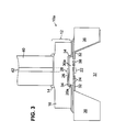
- FIG. 2 shows a cross-sectional view of an article according to the present invention comprising an optical fiber 40 having a core 42 in optical communication with a micro device 10.
- the optical fiber 40 may be single mode, multi-mode, plastic-coated silica fiber, plastic fiber and the like.
- an integrating arrangement 12 is used to make the optical fiber 40 an "integral" portion of the micro device 10.
- the word "integral" is meant to signify that there is, effectively, a fibermicro device interface, i.e., no gap exists nor is there a material layer between the core 42 and the micro device 10 having a refractive index different from that of the core 42.
- the integrating arrangement 12 includes a layer 14 of cement and a layer 16 of glass.
- the layers 14 and 16 are index-matched to that fiber core 42, i.e., the layers and the core have the same index of refraction.
- the glass layer 16 provides support for an adjacent layer of the micro device 10, as described further below.
- the fiber 40 is integrated with a micro device 10a operable to modulate an optical signal.
- the fiber 40 is in optical communication with at least a portion of a movable layer 20a.
- the movable layer 20a is supported at its periphery by a support layer 36.
- a well 37 defined within the support layer 36, is located beneath the movable layer 20a.
- the bottom 38 of the well 37 is defined by the movable layer 20a.
- the well 37 releases the movable layer 20a allowing it move vertically.
- the well 37 can be used for receiving a second optical fiber, not shown, if the micro-device 10a is operated in a transmissive mode.
- a nonmoving layer 26 is spaced from the movable layer 20a, creating a gap 30a therebetween. Damping holes 24 are provided to control ringing in the movable layer 20a, especially at operating frequencies above about 1-2 MHz.
- the layer 20a has a circular shape.
- micro-device 10a may suitably be structured, for example, as a Fabry-Perot device having equal reflectivity mirrors.
- An electrostatic force is thereby generated between those layers.
- the electrostatic force causes the movable layer 20a to move from its quiescent or equilibrium position towards the nonmoving layer 26.
- the change in position of the movable layer 20a results in a change in the size of the gap 30a.
- An optical signal can be modulated by controlling the change in reflectivity via the controlled voltage source.
- the nonmoving layer 26 and the movable layer 20a must be suitably conductive. If one or both of the layers 20a, 26 are not intrinsically conductive, or not capable of being rendered conductive by doping with suitable dopants, then an additional conductive layer is disposed adjacent to at least a portion of one or both of the layers 20a, 26.
- Conductive layers 32 and 34 are shown disposed adjacent to a portion of the respective movable and nonmoving layers.
- the conductive layers may be, for example, aluminum, gold or other suitable metals, or polysilicon. Using polysilicon as the material for the conductive layer 32 is convenient in the sense that the support layer 36 may be polysilicon.
- the conductive layer 32 can be formed by using a timed etch to prevent the etch from proceeding all the way through the support layer during well 37 formation.
- a thin layer of the support layer thus remains, serving as the conductive layer 32.
- such an etch must be timed.
- the optics expressions developed herein do not allow for such a layer.
- the movable and nonmoving layers must be optically transparent at the operating wavelength(s). More particularly, region 22 of the movable layer 20a and region 28 of the nonmoving layer 26, both in optical communication with the optical fiber core 42, must be optically transparent. If one or both of the conductive layers 32, 34 are present, and such layers are not optically transparent at the relevant wavelength(s), then such layers must not be present either below or above the regions 22 and 28 of the movable and nonmoving layers.
- the regions 22, 28 are referred to herein as an optical window.
- the micro-device 10 is fabricated using photolithographic methods. Briefly, a first layer of silicon nitride or polysilicon is deposited on a first side of a silicon wafer. That layer, when released, forms the movable layer 20a. A "pill" of a readily-etchable sacrificial material, such as, without limitation, silicon dioxide, phosphoro-silicate glass (PSG) or the like, is deposited on the first layer. A second layer, comprised of silicon nitride or polysilicon, is deposited on top of the pill. The materials choice for the second layer may be selected independently of the materials choice for the first layer. A layer 16 of glass is deposited over the second layer. The wafer is etched from the second side to the first layer.
- a readily-etchable sacrificial material such as, without limitation, silicon dioxide, phosphoro-silicate glass (PSG) or the like.
- PSG phosphoro-silicate glass
- a second layer comprised of silicon
- Holes 24 are etched into the first layer. Note that such holes must be etched through the conductive layer 32, if present. Etchant is delivered, through the holes 24, to the pill of sacrificial material sandwiched between the first and the second layer. The sacrificial material is etched away, releasing the first layer. The second layer is supported by the overlying layer 16 of glass. A layer 14 of cement, e.g. epoxy, is used for attaching the fiber 40 to the layer 16.
- a layer 14 of cement e.g. epoxy
- An alternate embodiment of the integrating arrangement 12 for use with suitably- structured micro-devices 10 does not require the layer 16 of glass.
- Such suitably-structured micro-devices 10 incorporate a nonmoving layer 26 that is, relatively speaking, thicker and/or of smaller diameter than the layer 26 present in devices requiring the layer 16.
- the optical performance of the article as modulator shown in FIG. 3 and described above can be characterized using expression [1].
- Expression [1] was developed based on the exemplary multi-layer article 4 shown in FIG. 1.
- the exemplary article shown in FIG. 3 is related to the article 4 as follows: the fiber core 42 and the integrating arrangement correspond to layer a, the nonmoving layer 26 corresponds to the layer b, the gap 30a corresponds to the layer c , the movable layer 20a corresponds to the layer d, and the well 37 beneath the movable layer 20a corresponds to the layer e.
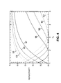
- the thickness t c of the gap 30a is equal to m ⁇ / ( 4n c ), where m is an even integer and ⁇ is the operating wavelength. Zero reflectivity is observed for each of such curves at a particular value of the refractive index n b of the layer b.
- the thickness t c of the gap 30a is equal to m ⁇ / (4n c ) , where m is an odd integer.
- the curves 51, 53, 55 and 57 show a significantly higher value of reflectivity at the same value of n b that resulted in zero reflectivity for curves 52, 54, 56 and 58.
- FIG. 4 indicates that very high contrast is obtained if the refractive index n b of the nonmoving layer 26 is an amount larger than the refractive index n d of the movable layer 20a.
- the gap 30a is equal to 3 ⁇ /(4 n c ) in the quiescent position.
- the gap 30a spacing is reduced to about 2 ⁇ /(4 n c ), which corresponds to zero reflectivity.
- the aforedescribed embodiment of the present invention can be operated in either a reflection mode with the single optical fiber 40, or in a transmissive mode wherein a second fiber to receive the modulated signal that is transmitted, in varying amounts, through the movable layer 20a. See, U.S. Patent Application 08/775,910 filed January 2, 1997.
- the fiber 40 is integrated with a micro-device 10b configured for measuring pressure.
- the micro-device 10b has a nonmoving layer 26 and a movable layer 20b, which layers are spaced forming chamber 30b therebetween.
- the chamber 30b is analogous to the gap 30a of the first exemplary embodiment.
- the movable layer 20b is supported at its periphery by support layer 36.
- a well 37 is defined within the support layer 36 underneath the movable layer 20b.
- Fiber 40 is attached to the micro-device 10b by integrating arrangement 12.
- the integrating arrangement preferably includes a layer 14 of cement and a layer 16 of glass.
- the layers 14 and 16 are index-matched to the fiber core 42.
- the exemplary configuration for measuring pressure shown in FIG. 5 is structurally similar to the configuration useful for optical signal modulation shown in FIG. 3. There are, however, some structural differences arising from the functional differences between those two configurations, as described below.
- the movable layer 20b is actuated or moved from an equilibrium position by the pressure exerted on it by a fluid in which the article is immersed.
- the pressure measuring configuration does not require any structure associated with applying a voltage to the movable and non-moving layers.
- the present article as configured for measuring pressure, is exceedingly small, e.g., as small as about 25 microns, and more typically 100+ microns, so as to cause reduced disturbances in the pressure-measuring environment.
- the only connection to the micro-device 10b incorporating the movable layer 20b is an optical fiber 40. This is particularly advantageous in applications in which the present article is intended to be placed well into a target environment, as opposed to being located along a vessel wall or the like.
- a second structural difference between the configuration for optical signal modulation and that for pressure measurement is that in the case of pressure measurement, there are no damping holes 24 in the movable membrane 20b. In other words, the chamber 30b is sealed.
- the operating principle underlying pressure measurement using the present invention is described below.
- the movable layer 20b As the movable layer 20b is exposed to a fluid pressure, it will move, i.e., bulge, towards the non-moving layer 26.
- the change in position of the movable layer 20b results in a change in the size of the chamber 30b.
- the reflectivity of micro device 10b changes. Such a change in reflectivity can be correlated to the pressure extant on the movable layer 20b.
- the mechanical response of an article configured for measuring pressure according to the present invention is described below.
- the chamber 30b is assumed to have a cylindrical geometry for the following mathematical analysis. It should be understood that such a geometry is not required. In cases where the geometry is not cylindrical, the following analysis must be appropriately changed.
- the chamber 30b is assumed to be evacuated.
- P d is equal to zero for a type I pressure measuring device.
- the chamber 30b is filled with a fixed amount of gas. For the type II pressure measuring device, the pressure P d inside the chamber 30b depends on the ambient temperature T and pressure P , on the mechanical properties of the movable layer 20b, and on the amount of gas sealed in the chamber 30b.
- u(r) is the displacement of the movable layer 20b at radial distance r from its center
- t m is the thickness of the movable layer 20b
- ⁇ is Poisson's ratio
- E Young's modulus
- ⁇ is the stretching force per unit length along the edge of the movable layer 20b
- f is an applied force per unit area.
- ⁇ S t m .
- f P - P d - ⁇ m g t m
- ⁇ m the average density of movable layer 20b.
- u mp [R 2 / (4 S t m )] ⁇ ( P - P d ) .
- [6] ( u mp / t o ) ⁇ [1 + ⁇ ( P/P p )] - [(1- ⁇ ( P/P p )) 2 + 4 ⁇ ( P o /P p ) ( T/T p )] 0.5 ⁇ / ( P/P o )
- P p packaging pressure
- T p the packaging temperature of the gas in the chamber 30b at the time the chamber is sealed.
- the movable layer 20b touches the non-moving layer 26 at P max .
- the midpoint displacement u mp ( P ) is given by expression [4] for a type I pressure measuring device and expressions [6] or [7] for a type II pressure measuring device. Substituting t c (P) into expression [1] gives the amplitude of the reflected light as a function of pressure.
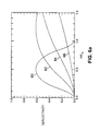
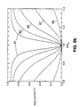
- FIGS. 6a, 6b and 7 show reflectivity versus P/P o ("the optical response")for a type I pressure measurement device according to the present invention.
- the pressuring measuring device is assumed to measure the pressure of a fluid having an optical index of water, i.e., about 1.33.
- the fiber core 42 and the integrating arrangement 12 correspond to layer a
- the nonmoving layer 26 corresponds to the layer b
- the chamber 30b corresponds to the layer c
- the movable layer 20b corresponds to the layer d
- the region 38 beneath the movable layer 20b corresponds to the layer e .
- the optical response shown in FIG. 6a is typical for a device in which the nonmoving and movable layers are formed of silicon nitride, which has a refractive index of about 2.0.
- ⁇ 0.5
- ⁇ of 0.1 provides the highest sensitivity, i.e., the greatest change in reflectivity for a given change in pressure, of the ⁇ values shown.
- the refractive indices used for FIG. 6b are typical for devices in which the nonmoving and movable layers are formed of polysilicon.
- a ⁇ of 0.05 provides the highest sensitivity of the ⁇ values shown.
- a chamber 30b having a greater height t o may suitably be used.
- a device can be designed to achieve a specific reflectivity at a particular ambient pressure by appropriately adjusting chamber height t o , as follows.
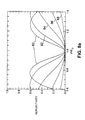
- FIG. 7 shows the optical response of a type I pressure measuring device for measuring pressures near 1 bar.
- Curves 70, 72, 74 are for ⁇ equals 0.2, 0.1 and 0.05, respectively.
- FIG. 7 shows that sensitivity increases with ⁇ . Sensitivity can be increased by increasing m to 4 or 6, etc.
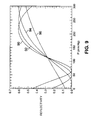
- FIGS. 8a, 8b and 9 show the optical response for a type II pressure measurement device according to the present invention.
- Curves 80, 82, 84, 86 and 88 show the optical response for ⁇ equals 1.0, 0.5, 0.2, 0.1 and 0.05, respectively.
- Curves 81, 83, 85, 87 and 89 show, respectively, the optical response for ⁇ equals 0.5, 0.2, 0.1, 0.05,and 0.02.
- P/P o 1
- movable layer 20b is flat so that the gap t c between the movable layer 20b and the nonmoving layer 26 is equal to the chamber height t c . As such, reflectivity is zero.
- t o [( m - ⁇ ) ⁇ /(4 n c )]/ ⁇ (- ⁇ P sel / P o ) + [(1 - ⁇ P sel / P ) 2 + 4 ⁇ ] 0.5 ⁇
- One exemplary nonlimiting use of the present type II pressure measuring device is for measuring blood pressure.
- the temperature control requirement is met by the known and stable temperature of the human or other type of animal body into which the device is inserted.
- the device is assumed to function with a midpoint pressure of 120 mm Hg.
- P sel / P o is equal to (760 + 120)/ 760 or about 1.15.
- Curves 90, 92, 94 and 96 show the optical response for ⁇ equals 2.0, 1.0, 0.5 and 0.2, respectively.
- Values of t o calculated from expression [14] are listed in TABLE 2.
- ⁇ t o / [ ⁇ /(4 n c )] t o microns 0.2 3.86 1.51 0.5 4.07 1.59 1.0 4.29 1.67 2.0 4.51 1.76 5.0 4.74 1.85
- the pressure measuring device is to useful over a range of about 50 to 300 mm Hg, then, with reference to FIG. 9, the device may be suitably constructed with a ⁇ of 0.5. A variation in temperature of 1°C would change the pressure reading by about 0.3 percent.
- the movable layer includes a plurality holes of appropriate number and size.
- a type III pressure measurement device can be used, for example, as a pressure surge indicator or microphone.
- the parameter ⁇ is a function of the several properties of the movable layer 30b; in particular, its thickness, diameter and stress.
- the displacement of the movable layer 30b depends linearly on the applied force.
- the stress due to displacement of the movable layer 30b must therefore be small compared to the intrinsic stress of the layer. This requires that u mp be sufficiently small compared to D.
- the device has a maximum usable pressure of about 1.3 bar.
- the midpoint displacement u mp of the movable layer is about 0.6 microns.
- the movable layer 20b of type I and II pressure measuring devices do not have damping holes, such as the damping holes 24 of the movable layer 20a of the article configured for optical modulation.
- a fabrication method different from that described for the optical modulation configuration is required. Such a method is described below.
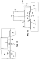
- FIG. 10 shows a side view of an arrangement of various material layers that can be used in fabricating pressure measuring devices according to the present invention.
- Layers shown in FIG. 10 include the support layer 360, typically silicon or polysilicon.
- a layer 200 a part of which forms the movable layer 20b after release, is deposited on the support layer 360.
- a sacrificial layer is deposited on a portion of the layer 200.
- the sacrificial layer is deposited to a thickness equivalent to the height t o of the chamber 30b.
- the sacrificial layer is patterned, typically photolithographically, to form a central "pill" 301 of material having four "arms" 303 depending therefrom, as shown in FIG. 11. As described in more detail below, the arms 303 are etched away to form access ways or channels for delivering etchant to the pill 301.
- the shape of the pill 301 defines the shape of the movable layer 20b.
- the pill 301 is circularly-shaped to define a circular movable layer 20b.
- four arms 303 are shown in FIG. 11, more or less of such arms may suitably be used for providing access channels to the pill 301.
- the pill 301 and arms 303 are shown in FIG. 10 as a sacrificial region 305.
- a layer 260 is deposited over the arms 303, the pill 301 and exposed regions of the layer 200.
- a layer 16 of glass e.g., silicon oxide, which was mentioned previously in conjunction with a description of the integrating arrangement 12, is deposited on top of the layer 260.
- the layer 16 is in the range of from about 10 to 15 microns in thickness, though greater or less thicknesses may suitably be used.
- the layers 200 and 260 can be formed from materials such as, without limitation, silicon oxide, polysilicon, or, more preferably, silicon nitride.
- Access wells 307 are formed through the layer 16 and the layer 260 to communicate with the arms 303.
- the access wells 307 can be formed by etching with an appropriate wet or dry etch.
- An exemplary wet etch suitable for etching the layers include HF-based solutions, and exemplary dry etches include fluorine-containing gasses, such as, for example, sulfur hexafluoride and carbontetrafluoride.
- the access wells are preferably about 3 to 10 microns in diameter.
- the arms 303 can be accessed from the side rather than from above.
- the chamber 30b is formed by removing the pill 301.
- etchant is delivered through the access wells 307 to the arms 303. Since the arms 303 and pill 301 are formed of a material that etches rapidly compared with the surrounding material, e.g., silicon nitride, silicon oxide and the like, the arms 303 form channels in the surrounding material as they are etched.
- the arms 303 may suitably be patterned to have a width of about 5 to 10 microns and a height equivalent to the height of the pill 301. After the arms 303 are completely removed by the etchant, the channels formed thereby lead to the pill 301.
- Etchant is delivered through the channels to the pill 301, which is selectively etched in preference to the surrounding material layers 200, 260.
- the support layer 360, the pill 301 and the arms 303 are polysilicon and the movable layer 20b is silicon nitride.
- Etchants useful for removing polysilicon include potassium hydroxide, ethylene diamine pyrocatechol (EDP) and hydrazine.
- the aforementioned polysilicon etchants etch polysilicon at a much faster rate than either silicon nitride or silicon oxide.
- the etch to remove the pill 301 does not require careful timing.
- the layer 16, which is typically silicon oxide can be deposited before removing the pill 301. Depositing the layer 16 after removing the pill 301 is problematic.
- PSG can be used for the sacrificial layer, which can be etched using hydrofluoric acid. After removing the pill 301, the access wells 307 may be filled with an epoxy. Alternatively, glass can be sputter deposited over the micro-device.
- the well 37 is required, in conjunction with the gap 30b, for forming the movable layer 20b.
- Etchant suitable for etching the support layer 360 is selected as a function of the material used for the support layer. Such selection is within the capabilities of those ordinarily skilled in the art.
- FIG. 12 shows the micro-device 10b after gap and well formation.
- the fiber 40 is integrated with a micro-device 10c configured for measuring temperature.
- the micro-device 10c has a nonmoving layer 26 and a movable layer 20c, which layers are spaced forming chamber 30c therebetween.
- the movable layer- 20b is supported at its periphery by support layer 36.
- Fiber 40 is attached to the micro-device 10c by integrating arrangement 12.
- the integrating arrangement preferably includes a layer 14 of cement and a layer 16 of glass.
- the layers 14 and 16 are index-matched to that fiber core 42, i.e., the layers and the core have the same index of refraction.
- a cavity 33 is formed within the support layer 36 beneath the movable layer 20c.
- the cavity 33 is evacuated.
- the cavity 33 isolates the chamber 30c from variations in the ambient pressure.
- the movable layer 30c moves only in response to temperature changes that alter the pressure in the gas-filled chamber 30c.
- the change in position of the movable layer 20c results in a change in the size of the chamber 30c.
- the reflectivity of micro device 10c changes. Such a change in reflectivity can be correlated to the ambient temperature T .
- the cavity 33 which corresponds to the "e" layer shown in FIG. 1, has an optical index of 1.
- a device can be designed to provide a preselected reflectivity for a given temperature T sel .
- T sel a preselected reflectivity for a given temperature T sel .
- t o [( m + ⁇ ) ⁇ /(4 n c )]/(1 + 4 ⁇ T sel / T p ) 0.5
- Chamber height t o for a variety of values of ⁇ are shown in TABLE 4.
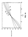
- Expression [17] was used to calculate t o and expressions [1], [11] and [16] were used to generate the optical response curves shown in FIG. 14.
- Curves 110, 112, 114, 116 and 118 show the optical response for ⁇ equals 0.1, 0.2, 0.5, 1.0 and 10.0, respectively
- a temperature measuring device can be formed using a method very similar to that used for fabricating the present type I and II pressure measuring devices.
- the fabrication method must be modified to provide the cavity 33. This may be simply accomplished by forming the well 37 as described in previous embodiments and then "capping" it, such as by bonding a silicon wafer over the mouth of the well.
- the devices described in Sections I - III above can be advantageously formed into arrays. Such arrays can be used, for example, to provide a pressure or temperature profile of a very localized phenomenon.
- a plurality of pressure or temperature measuring devices are fabricated on a wafer. One or more of such wafers are formed and embedded in, or disposed on, a surface exposed to the environment to be measured.
- An optical signal reflected from the movable layer (or transmitted through it for transmissive device) of each device is guided by the optical fiber to a photodetector array.
- the photodetector array is operable to measure the optical signal delivered from each optical fiber.
- An electrical signal corresponding to measured optical signal is produced by the photodetector array and delivered to a processor operable to convert the signal information to a temperature or pressure using data developed according to the present invention.
- At least one pressure measurement device and one temperature measurement device according to the present invention are fabricated in close proximity to one another on a single chip. Such an arrangement provides the ability to measure the temperature and pressure of an environment at nearly the same location. Fabrication of wafers possessing more than one type of measurement device can be accomplished by cofabrication or by using flip-chip bonding methods, which are generally well known. For a description of a flip-chip bonding method for forming chips containing more than one type of device, see U.S. Patent Application 08/766,214 filed December 12, 1996 and entitled HYBRID CHIP AND METHOD THEREFOR.
Landscapes
- Physics & Mathematics (AREA)
- General Physics & Mathematics (AREA)
- Optics & Photonics (AREA)
- Spectroscopy & Molecular Physics (AREA)
- Mechanical Light Control Or Optical Switches (AREA)
- Length Measuring Devices By Optical Means (AREA)
- Measuring Fluid Pressure (AREA)
Applications Claiming Priority (2)
| Application Number | Priority Date | Filing Date | Title |
|---|---|---|---|
| US883740 | 1992-05-15 | ||
| US08/883,740 US5831262A (en) | 1997-06-27 | 1997-06-27 | Article comprising an optical fiber attached to a micromechanical device |
Publications (2)
| Publication Number | Publication Date |
|---|---|
| EP0887675A2 true EP0887675A2 (de) | 1998-12-30 |
| EP0887675A3 EP0887675A3 (de) | 1999-06-09 |
Family
ID=25383246
Family Applications (1)
| Application Number | Title | Priority Date | Filing Date |
|---|---|---|---|
| EP98304774A Ceased EP0887675A3 (de) | 1997-06-27 | 1998-06-17 | Gegenstand bestehend aus einer an einer mikromechanischen Vorrichtung befestigten optischen Faser |
Country Status (3)
| Country | Link |
|---|---|
| US (1) | US5831262A (de) |
| EP (1) | EP0887675A3 (de) |
| JP (1) | JP3311680B2 (de) |
Families Citing this family (74)
| Publication number | Priority date | Publication date | Assignee | Title |
|---|---|---|---|---|
| US6552469B1 (en) * | 1998-06-05 | 2003-04-22 | Knowles Electronics, Llc | Solid state transducer for converting between an electrical signal and sound |
| US6321010B1 (en) | 1999-08-30 | 2001-11-20 | Lucent Technologies Inc. | Optical microstructure and method of manufacture |
| AU1786301A (en) * | 1999-12-02 | 2001-06-12 | Tegal Corporation | Improved reactor with heated and textured electrodes and surfaces |
| US6590710B2 (en) * | 2000-02-18 | 2003-07-08 | Yokogawa Electric Corporation | Fabry-Perot filter, wavelength-selective infrared detector and infrared gas analyzer using the filter and detector |
| US6377718B1 (en) | 2000-03-24 | 2002-04-23 | Wisconsin Alumni Research Foundation | Micromechanical phase-shifting gate optical modulator |
| US6506289B2 (en) | 2000-08-07 | 2003-01-14 | Symmorphix, Inc. | Planar optical devices and methods for their manufacture |
| US6987859B2 (en) | 2001-07-20 | 2006-01-17 | Knowles Electronics, Llc. | Raised microstructure of silicon based device |
| US6535460B2 (en) | 2000-08-11 | 2003-03-18 | Knowles Electronics, Llc | Miniature broadband acoustic transducer |
| US7434305B2 (en) | 2000-11-28 | 2008-10-14 | Knowles Electronics, Llc. | Method of manufacturing a microphone |
| US8629005B1 (en) | 2000-11-28 | 2014-01-14 | Knowles Electronics, Llc | Methods of manufacture of bottom port surface mount silicon condenser microphone packages |
| US7439616B2 (en) * | 2000-11-28 | 2008-10-21 | Knowles Electronics, Llc | Miniature silicon condenser microphone |
| US7166910B2 (en) * | 2000-11-28 | 2007-01-23 | Knowles Electronics Llc | Miniature silicon condenser microphone |
| US6533907B2 (en) | 2001-01-19 | 2003-03-18 | Symmorphix, Inc. | Method of producing amorphous silicon for hard mask and waveguide applications |
| US7469558B2 (en) | 2001-07-10 | 2008-12-30 | Springworks, Llc | As-deposited planar optical waveguides with low scattering loss and methods for their manufacture |
| US7404877B2 (en) | 2001-11-09 | 2008-07-29 | Springworks, Llc | Low temperature zirconia based thermal barrier layer by PVD |
| US7023066B2 (en) * | 2001-11-20 | 2006-04-04 | Knowles Electronics, Llc. | Silicon microphone |
| US6884327B2 (en) | 2002-03-16 | 2005-04-26 | Tao Pan | Mode size converter for a planar waveguide |
| US7378356B2 (en) | 2002-03-16 | 2008-05-27 | Springworks, Llc | Biased pulse DC reactive sputtering of oxide films |
| US8021778B2 (en) | 2002-08-09 | 2011-09-20 | Infinite Power Solutions, Inc. | Electrochemical apparatus with barrier layer protected substrate |
| US8404376B2 (en) | 2002-08-09 | 2013-03-26 | Infinite Power Solutions, Inc. | Metal film encapsulation |
| US8445130B2 (en) | 2002-08-09 | 2013-05-21 | Infinite Power Solutions, Inc. | Hybrid thin-film battery |
| US8236443B2 (en) | 2002-08-09 | 2012-08-07 | Infinite Power Solutions, Inc. | Metal film encapsulation |
| US8394522B2 (en) | 2002-08-09 | 2013-03-12 | Infinite Power Solutions, Inc. | Robust metal film encapsulation |
| US8431264B2 (en) | 2002-08-09 | 2013-04-30 | Infinite Power Solutions, Inc. | Hybrid thin-film battery |
| US9793523B2 (en) | 2002-08-09 | 2017-10-17 | Sapurast Research Llc | Electrochemical apparatus with barrier layer protected substrate |
| US20070264564A1 (en) | 2006-03-16 | 2007-11-15 | Infinite Power Solutions, Inc. | Thin film battery on an integrated circuit or circuit board and method thereof |
| WO2004021532A1 (en) | 2002-08-27 | 2004-03-11 | Symmorphix, Inc. | Optically coupling into highly uniform waveguides |
| US6781231B2 (en) * | 2002-09-10 | 2004-08-24 | Knowles Electronics Llc | Microelectromechanical system package with environmental and interference shield |
| KR100691168B1 (ko) | 2003-02-27 | 2007-03-09 | 섬모픽스, 인코포레이티드 | 유전 장벽층 필름 |
| US7238628B2 (en) | 2003-05-23 | 2007-07-03 | Symmorphix, Inc. | Energy conversion and storage films and devices by physical vapor deposition of titanium and titanium oxides and sub-oxides |
| US8728285B2 (en) | 2003-05-23 | 2014-05-20 | Demaray, Llc | Transparent conductive oxides |
| US20040263857A1 (en) * | 2003-06-24 | 2004-12-30 | Basavanhally Nagesh R. | Fiber-optic gauge having one or more side-mounted sensors |
| JP4112505B2 (ja) * | 2004-01-14 | 2008-07-02 | 株式会社東芝 | 光マイクロフォン及びその製造方法 |
| US7087134B2 (en) * | 2004-03-31 | 2006-08-08 | Hewlett-Packard Development Company, L.P. | System and method for direct-bonding of substrates |
| US7959769B2 (en) | 2004-12-08 | 2011-06-14 | Infinite Power Solutions, Inc. | Deposition of LiCoO2 |
| EP1825545B1 (de) | 2004-12-08 | 2009-11-04 | Symmorphix, Inc. | Abscheidung von licoo2 |
| US7379629B1 (en) | 2004-12-12 | 2008-05-27 | Burns David W | Optically coupled resonant pressure sensor |
| US7176048B1 (en) | 2004-12-12 | 2007-02-13 | Burns David W | Optically coupled sealed-cavity resonator and process |
| US7499604B1 (en) | 2004-12-12 | 2009-03-03 | Burns David W | Optically coupled resonant pressure sensor and process |
| US7443509B1 (en) | 2004-12-12 | 2008-10-28 | Burns David W | Optical and electronic interface for optically coupled resonators |
| US7605391B2 (en) * | 2004-12-12 | 2009-10-20 | Burns David W | Optically coupled resonator |
| DE102005008512B4 (de) | 2005-02-24 | 2016-06-23 | Epcos Ag | Elektrisches Modul mit einem MEMS-Mikrofon |
| DE102005008511B4 (de) | 2005-02-24 | 2019-09-12 | Tdk Corporation | MEMS-Mikrofon |
| US7838133B2 (en) | 2005-09-02 | 2010-11-23 | Springworks, Llc | Deposition of perovskite and other compound ceramic films for dielectric applications |
| DE102005053767B4 (de) | 2005-11-10 | 2014-10-30 | Epcos Ag | MEMS-Mikrofon, Verfahren zur Herstellung und Verfahren zum Einbau |
| DE102005053765B4 (de) | 2005-11-10 | 2016-04-14 | Epcos Ag | MEMS-Package und Verfahren zur Herstellung |
| US7583390B2 (en) * | 2006-03-02 | 2009-09-01 | Symphony Acoustics, Inc. | Accelerometer comprising an optically resonant cavity |
| US7355723B2 (en) * | 2006-03-02 | 2008-04-08 | Symphony Acoustics, Inc. | Apparatus comprising a high-signal-to-noise displacement sensor and method therefore |
| US7359067B2 (en) * | 2006-04-07 | 2008-04-15 | Symphony Acoustics, Inc. | Optical displacement sensor comprising a wavelength-tunable optical source |
| US7551295B2 (en) * | 2006-06-01 | 2009-06-23 | Symphony Acoustics, Inc. | Displacement sensor |
| US7894618B2 (en) * | 2006-07-28 | 2011-02-22 | Symphony Acoustics, Inc. | Apparatus comprising a directionality-enhanced acoustic sensor |
| US20080042223A1 (en) * | 2006-08-17 | 2008-02-21 | Lu-Lee Liao | Microelectromechanical system package and method for making the same |
| US20080075308A1 (en) * | 2006-08-30 | 2008-03-27 | Wen-Chieh Wei | Silicon condenser microphone |
| JP2010505044A (ja) | 2006-09-29 | 2010-02-18 | インフィニット パワー ソリューションズ, インコーポレイテッド | フレキシブル基板のマスキングおよびフレキシブル基板上にバッテリ層を堆積させるための材料拘束 |
| US20080083957A1 (en) * | 2006-10-05 | 2008-04-10 | Wen-Chieh Wei | Micro-electromechanical system package |
| US7894622B2 (en) | 2006-10-13 | 2011-02-22 | Merry Electronics Co., Ltd. | Microphone |
| US8197781B2 (en) | 2006-11-07 | 2012-06-12 | Infinite Power Solutions, Inc. | Sputtering target of Li3PO4 and method for producing same |
| US7626707B2 (en) * | 2007-10-29 | 2009-12-01 | Symphony Acoustics, Inc. | Dual cavity displacement sensor |
| US8007609B2 (en) * | 2007-10-31 | 2011-08-30 | Symphony Acoustics, Inc. | Parallel plate arrangement and method of formation |
| KR20100102180A (ko) | 2007-12-21 | 2010-09-20 | 인피니트 파워 솔루션스, 인크. | 전해질 막을 위한 표적을 스퍼터링하는 방법 |
| US8268488B2 (en) | 2007-12-21 | 2012-09-18 | Infinite Power Solutions, Inc. | Thin film electrolyte for thin film batteries |
| JP5705549B2 (ja) | 2008-01-11 | 2015-04-22 | インフィニット パワー ソリューションズ, インコーポレイテッド | 薄膜電池および他のデバイスのための薄膜カプセル化 |
| WO2009124191A2 (en) | 2008-04-02 | 2009-10-08 | Infinite Power Solutions, Inc. | Passive over/under voltage control and protection for energy storage devices associated with energy harvesting |
| WO2010019577A1 (en) | 2008-08-11 | 2010-02-18 | Infinite Power Solutions, Inc. | Energy device with integral collector surface for electromagnetic energy harvesting and method thereof |
| KR101613671B1 (ko) | 2008-09-12 | 2016-04-19 | 사푸라스트 리써치 엘엘씨 | 전자기 에너지에 의해 데이터 통신을 하는 통합 도전성 표면을 가진 에너지 장치 및 그 통신 방법 |
| WO2010042594A1 (en) | 2008-10-08 | 2010-04-15 | Infinite Power Solutions, Inc. | Environmentally-powered wireless sensor module |
| JP2010164596A (ja) * | 2009-01-13 | 2010-07-29 | Nec Corp | 光機能集積デバイス |
| US8599572B2 (en) | 2009-09-01 | 2013-12-03 | Infinite Power Solutions, Inc. | Printed circuit board with integrated thin film battery |
| US20110169724A1 (en) * | 2010-01-08 | 2011-07-14 | Qualcomm Mems Technologies, Inc. | Interferometric pixel with patterned mechanical layer |
| WO2011156392A1 (en) | 2010-06-07 | 2011-12-15 | Infinite Power Solutions, Inc. | Rechargeable, high-density electrochemical device |
| US9374643B2 (en) | 2011-11-04 | 2016-06-21 | Knowles Electronics, Llc | Embedded dielectric as a barrier in an acoustic device and method of manufacture |
| US9078063B2 (en) | 2012-08-10 | 2015-07-07 | Knowles Electronics, Llc | Microphone assembly with barrier to prevent contaminant infiltration |
| DE102013106353B4 (de) * | 2013-06-18 | 2018-06-28 | Tdk Corporation | Verfahren zum Aufbringen einer strukturierten Beschichtung auf ein Bauelement |
| US9794661B2 (en) | 2015-08-07 | 2017-10-17 | Knowles Electronics, Llc | Ingress protection for reducing particle infiltration into acoustic chamber of a MEMS microphone package |
Citations (6)
| Publication number | Priority date | Publication date | Assignee | Title |
|---|---|---|---|---|
| US4682500A (en) * | 1985-04-11 | 1987-07-28 | Sharp Kabushiki Kaisha | Pressure sensitive element |
| US4983824A (en) * | 1989-07-06 | 1991-01-08 | Metricor Inc. | Optically resonant sensor with increased monotonic range |
| EP0571107A1 (de) * | 1992-05-19 | 1993-11-24 | Vaisala Technologies Inc., Oy | Optischer Kraftwandler mit Fabry-Perot Resonator und einem weiteren abtastendem Fabry-Perot Resonator |
| US5280173A (en) * | 1992-01-31 | 1994-01-18 | Brown University Research Foundation | Electric and electromagnetic field sensing system including an optical transducer |
| EP0729051A2 (de) * | 1995-02-21 | 1996-08-28 | Ascom Tech Ag | Optischer Spiegelmodulator |
| US5589974A (en) * | 1994-01-27 | 1996-12-31 | Lucent Technologies Inc. | Micromechanical modulator |
Family Cites Families (1)
| Publication number | Priority date | Publication date | Assignee | Title |
|---|---|---|---|---|
| US4655544A (en) * | 1985-01-23 | 1987-04-07 | Galvin John J | Electrical shock proof fiber optic control system |
-
1997
- 1997-06-27 US US08/883,740 patent/US5831262A/en not_active Expired - Lifetime
-
1998
- 1998-06-17 EP EP98304774A patent/EP0887675A3/de not_active Ceased
- 1998-06-26 JP JP18041598A patent/JP3311680B2/ja not_active Expired - Fee Related
Patent Citations (6)
| Publication number | Priority date | Publication date | Assignee | Title |
|---|---|---|---|---|
| US4682500A (en) * | 1985-04-11 | 1987-07-28 | Sharp Kabushiki Kaisha | Pressure sensitive element |
| US4983824A (en) * | 1989-07-06 | 1991-01-08 | Metricor Inc. | Optically resonant sensor with increased monotonic range |
| US5280173A (en) * | 1992-01-31 | 1994-01-18 | Brown University Research Foundation | Electric and electromagnetic field sensing system including an optical transducer |
| EP0571107A1 (de) * | 1992-05-19 | 1993-11-24 | Vaisala Technologies Inc., Oy | Optischer Kraftwandler mit Fabry-Perot Resonator und einem weiteren abtastendem Fabry-Perot Resonator |
| US5589974A (en) * | 1994-01-27 | 1996-12-31 | Lucent Technologies Inc. | Micromechanical modulator |
| EP0729051A2 (de) * | 1995-02-21 | 1996-08-28 | Ascom Tech Ag | Optischer Spiegelmodulator |
Non-Patent Citations (2)
| Title |
|---|
| CHAN M A ET AL: "A MICROMACHINED PRESSURE SENSOR WITH FIBER-OPTIC INTERFEROMETRIC READOUT" SENSORS AND ACTUATORS A, vol. A43, no. 1/03, 1 May 1994, pages 196-201, XP000454110 * |
| XIAO Z ET AL: "A FIBER OPTICAL VOLTAGE SENSOR PREPARED BY MICROMACHINING AND WAFER BONDING" SENSORS AND ACTUATORS A, vol. A41, no. 1/03, 1 April 1994, pages 334-337, XP000450051 * |
Also Published As
| Publication number | Publication date |
|---|---|
| JPH1195131A (ja) | 1999-04-09 |
| US5831262A (en) | 1998-11-03 |
| EP0887675A3 (de) | 1999-06-09 |
| JP3311680B2 (ja) | 2002-08-05 |
Similar Documents
| Publication | Publication Date | Title |
|---|---|---|
| US5831262A (en) | Article comprising an optical fiber attached to a micromechanical device | |
| JP6084672B2 (ja) | 光ファイバ適合音響センサ | |
| CA2537214C (en) | Optical fiber pressure and acceleration sensor fabricated on a fiber endface | |
| US8542365B2 (en) | Optical MEMS chemical sensor array | |
| US6539136B1 (en) | Fiber-optic pressure sensor, variants and method for producing a resilient membrane | |
| US8559770B2 (en) | Fabry-perot optical sensor and method of manufacturing the same | |
| US7796267B2 (en) | System, method and apparatus for a micromachined interferometer using optical splitting | |
| WO2000025103A1 (en) | Methods and apparatus for mechanically enhancing the sensitivity of transversely loaded fiber optic sensors | |
| EP2859315B1 (de) | Optischer mems-sensor | |
| US9823150B2 (en) | Micro-machined optical pressure sensors | |
| US5569856A (en) | Differential pressure transducer wherein a bridge connects two pressure diaphragms | |
| US6321010B1 (en) | Optical microstructure and method of manufacture | |
| WO2015080663A1 (en) | Micro-machined optical pressure sensors | |
| Greywall | Micromechanical light modulators, pressure gauges, and thermometers attached to optical fibers | |
| Lai et al. | Study on optical fiber pressure sensors with temperature-insensitivity based on Fabry-Pérot interferometry | |
| US6320992B1 (en) | Integrated optic accelerometer and method | |
| Han et al. | Deflection behavior of Fabry-Perot pressure sensors having planar and corrugated membrane | |
| CN113884703B (zh) | 一种三轴光纤加速度计 | |
| Kim et al. | Micromachined Fabry-Perot cavity pressure transducer with optical fiber interconnects | |
| Leinders | Characterization of a novel optical micro-machined ultrasound transducer | |
| Józwik et al. | Microsystem based optical measurement systems: case of opto-mechanical sensors | |
| Hartl et al. | Model of a microminiaturized pressure sensor with optical output | |
| Han | Fabry-Perot pressure and chemical sensors by silicon micromachining techniques |
Legal Events
| Date | Code | Title | Description |
|---|---|---|---|
| PUAI | Public reference made under article 153(3) epc to a published international application that has entered the european phase |
Free format text: ORIGINAL CODE: 0009012 |
|
| AK | Designated contracting states |
Kind code of ref document: A2 Designated state(s): DE FR GB |
|
| AX | Request for extension of the european patent |
Free format text: AL;LT;LV;MK;RO;SI |
|
| PUAL | Search report despatched |
Free format text: ORIGINAL CODE: 0009013 |
|
| AK | Designated contracting states |
Kind code of ref document: A3 Designated state(s): AT BE CH CY DE DK ES FI FR GB GR IE IT LI LU MC NL PT SE |
|
| AX | Request for extension of the european patent |
Free format text: AL;LT;LV;MK;RO;SI |
|
| RIC1 | Information provided on ipc code assigned before grant |
Free format text: 6G 02B 26/02 A, 6G 02B 6/42 B, 6G 01L 9/00 B, 6G 01D 5/26 B |
|
| 17P | Request for examination filed |
Effective date: 19991126 |
|
| AKX | Designation fees paid |
Free format text: DE FR GB |
|
| 17Q | First examination report despatched |
Effective date: 20021107 |
|
| STAA | Information on the status of an ep patent application or granted ep patent |
Free format text: STATUS: THE APPLICATION HAS BEEN REFUSED |
|
| 18R | Application refused |
Effective date: 20060115 |