EP0886231A2 - Kreditkartenterminal-Gerät - Google Patents
Kreditkartenterminal-Gerät Download PDFInfo
- Publication number
- EP0886231A2 EP0886231A2 EP98101189A EP98101189A EP0886231A2 EP 0886231 A2 EP0886231 A2 EP 0886231A2 EP 98101189 A EP98101189 A EP 98101189A EP 98101189 A EP98101189 A EP 98101189A EP 0886231 A2 EP0886231 A2 EP 0886231A2
- Authority
- EP
- European Patent Office
- Prior art keywords
- assembly
- card
- printed substrate
- terminal apparatus
- control printed
- Prior art date
- Legal status (The legal status is an assumption and is not a legal conclusion. Google has not performed a legal analysis and makes no representation as to the accuracy of the status listed.)
- Granted
Links
Images


Classifications
-
- G—PHYSICS
- G06—COMPUTING; CALCULATING OR COUNTING
- G06K—GRAPHICAL DATA READING; PRESENTATION OF DATA; RECORD CARRIERS; HANDLING RECORD CARRIERS
- G06K7/00—Methods or arrangements for sensing record carriers, e.g. for reading patterns
- G06K7/0013—Methods or arrangements for sensing record carriers, e.g. for reading patterns by galvanic contacts, e.g. card connectors for ISO-7816 compliant smart cards or memory cards, e.g. SD card readers
Definitions
- the present invention relates to a card terminal apparatus, and, in particular, to a card terminal apparatus, into which a card is inserted, and which is applied to an electronic money system in which giving and receiving of money is performed by giving and receiving electronic information.
- an electronic money system is being developed.
- an IC chip is embedded in an IC card, and money in a form of electronic information is stored therein.
- a terminal apparatus for writing information in and reading information from the IC chip of the IC card is set in each house and each store.
- a system in which computers, for managing the respective card terminal apparatuses and the information of the IC cards, are connected with each other via a network, is used.
- the card terminal apparatus of one type is a horizontal placement type one, in which the operation surface thereof lies horizontally
- the card terminal apparatus of the other type is a vertical placement type one, in which the operation surface thereof stands vertically.
- the card terminal apparatus of the horizontal placement type is placed on a table or the like and used.
- the card terminal apparatus of the vertical placement type is hanged on a wall or the like and used.
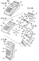
- FIG.1A shows a card terminal apparatus 10 of the horizontal placement type in the related art
- FIG.1B shows a card terminal apparatus 20 of the vertical placement type in the related art.
- the terminal apparatus 10 of the horizontal placement type is, in consideration of operational convenience, in a condition where it is placed on a table 40.
- An input key portion 12 and a liquid crystal display portion 13 are arranged on the operator side (X 1 side), and an IC card insertion hole 14 is arranged at a portion near to the head (X 2 side).
- An IC card 30 is inserted into the IC card insertion hole 14 from the top side in the position in which an operator can see an IC chip 31.
- the terminal apparatus 20 of the vertical placement type is, in consideration of operational convenience, in a condition where it is hung on a wall 41.
- An IC card insertion hole 24 is arranged at a portion near to the bottom (Z 2 side), a liquid crystal display portion 23 is arranged at the head side (Z 1 side), and an input key portion 22 is arranged between the IC card insertion hole 24 and the liquid crystal display portion 23.
- the IC card 30 is inserted into the IC card insertion hole 24 from the front side in the position in which an operator can see the IC chip 31.
- the card terminal apparatus 10 of the horizontal placement type is different from the card terminal apparatus 20 of the vertical placement type, and there are problems as described below.
- the card terminal apparatus 10 of the horizontal placement type When the card terminal apparatus 10 of the horizontal placement type is used in a vertical placement condition, it is difficult to operate the terminal apparatus 10 because, for example, the positions of the keys are reversed. Thus, it is impractical to use the card terminal apparatus 10 of the horizontal placement type in the vertical placement condition. Similarly, when the card terminal apparatus 20 of the vertical placement type is used in a horizontal placement condition, it is difficult to operate the terminal apparatus 10. Thus, it is impractical to use the card terminal apparatus 20 of the vertical placement type in the horizontal placement condition.
- An object of the present invention is to provide a card terminal apparatus which solve the above-mentioned problems by improving setting convenience.
- a card terminal apparatus comprises:
- the card terminal apparatuses can be shipped. Thereby, it is possible to perform speedy delivery and setting of the card terminal apparatuses in accordance with a client's requests.
- change of the setting type of the card terminal apparatus in accordance with a client's request after once assembling the apparatus can be relatively easily performed. Further, only two metallic molds for resin molding are necessary for molding the first assembly and the second assembly. Accordingly, the costs for the metallic molds are inexpensive.
- the second assembly has an input key, liquid crystal display panel and control printed substrate unit inside thereof, the input key, liquid crystal panel and control printed substrate unit integrally having input keys, a liquid crystal display panel and a control printed substrate.
- FIGS.2A, 2B, 2C, 2D and 2E show assembling of a card terminal apparatus 50H of a horizontal placement type and a card terminal apparatus 50V of a vertical placement type in a first embodiment of the present invention.
- Each of the card terminal apparatus 50H of the horizontal placement type and the card terminal apparatus 50V of the vertical placement type is a combination of a first assembly 51 and a second assembly 52.
- X 1 and X 2 are the longitudinal directions of the first assembly 51 and the second assembly 52, and Y 1 and Y 2 are the width directions thereof.
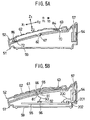
- the first assembly 51 includes, as also shown in FIGS.5A and 5B, generally, a long and thin case 53 made of synthetic resin, an IC card reading and writing unit 54 and a control printed substrate 55 having a control circuit, which are contained in the case 53.
- the case 53 has an IC card insertion hole 57 and a second-assembly loading portion 58 on the top surface thereof.
- the IC card reading and writing unit 54 is located at the depth of the IC card insertion hole 57.
- the IC card reading and writing unit 54 is connected with the control printed substrate 55 via a cable 200, and an external connector 201 for connecting the apparatus with a personal computer or the like is connected with the control printed substrate 55 via a cable 202.
- the bottom surface of the case 53 is covered by a bottom plate 59.
- the second assembly 52 has, generally, a board-like rectangular shape.
- an input key and liquid crystal display panel unit 61 which integrally has input keys and a liquid crystal display panel, is assembled.
- the second assembly 52 has, on the case 60, input key portions 62 and a liquid crystal display portion 63.
- the liquid crystal display portion 63 is located at a portion near to P1 and the input key portions 62 occupy a wide area from the position of P2 to the liquid crystal display portion 63.
- the second assembly 52 curves to correspond to a part of the cylindrical surface of a cylinder having a large radius of curvature.
- the curving is such that the surface of the second assembly 52, on which the input key portions 62 and the liquid crystal display portion 63 are provided, is convex.
- an opening 66 is formed at the center thereof.
- rectangular holding holes 67, 68, and rectangular engaging holes 70, 71, 72 and 73 are formed.
- the holding holes 67 and 68 are formed on the Y 1 , Y 2 sides about the center O 2 .
- the engaging holes 70, 71, 72 and 73 are formed in proximity to the respective corners of the second assembly 52.
- the holding holes 67 and 68 are arranged point-symmetrically about the center O 2 .
- the engaging holes 70 and 73 are arranged point-symmetrically about the center O 2 .
- the engaging holes 71 and 72 are arranged point-symmetrically about the center O 2 .
- the top surface of the case 53 of the first assembly 51 inclines downwardly along the X 1 direction from one end to the other end.
- the card insertion hole 57 is located on the top surface of the case 53 at the Q1 side at which the case 53 is relatively thick along the longitudinal direction of the case 53.
- the second-assembly loading portion 58 has a size corresponding to the size of the second assembly 52, has an approximately rectangular shape, and has a surface 80 (outward-curved surface corresponding to a part of the cylindrical surface of a cylinder having a large radius of curvature) corresponding to the inward-curved surface 65 of the curved second assembly 52.
- the second-assembly loading portion 58 has an opening 81 at the center O 1 thereof.
- holding nails 82 and 83, and hooks 84, 85, 86 and 87 are formed.
- the holding nails 82 and 83 are arranged in the Y 1 and Y 2 directions about the center O 1 , and have elasticity in the Z 1 and Z 2 directions (vertical direction with respect to the surface 80).
- the hooks 84, 85, 86 and 87 are L-shaped, respectively, and are located in proximity to the respective corners of the second-assembly loading portion 58.
- the L-shaped hooks 84, 85, 86 and 87 face the same direction (direction toward Q2), respectively.
- the holding nails 82 and 83 are arranged point-symmetrically about the center O 1 .
- the hooks 84 and 87 are arranged point-symmetrically about the center O 1 .
- the hooks 85 and 86 are arranged point-symmetrically about the center O 1 .
- Positional relationship is such that the holding holes 67 and 68 correspond to the holding nails 82 and 83, respectively, and the engaging holes 70, 71, 72, 73 correspond to the hooks 84, 85, 86 and 87, respectively.
- FIGS.4, 5A and 5B show the card terminal apparatus 50H of the horizontal placement type.
- the first assembly 51 is in the position in which the IC card insertion hole 57 is located at the X 2 -direction end.
- the second assembly 52 is loaded in the position in which the liquid crystal display portion 63 is located at the X 2 -direction end.
- the crystal display portion 63 of the second assembly 52 is adjacent to the IC card insertion hole 57 of the first assembly 51.
- the thus-assembled card terminal apparatus 50H in the horizontal placement type is, as shown in FIG.4, in the condition where the apparatus 50H is placed on a table 40, the input key portions 62 are arranged at an operator side (X 1 side), the liquid crystal display portion 63 is arranged at the rear side of the input key portions 62, and the IC card insertion hole 57 is arranged at the further rear side.
- the IC card 30 is inserted into the IC card insertion hole 57 from the top side in the position in which an operator can see the IC chip 31.
- FIGS.6, 7A and 7B show the card terminal apparatus 50V in the vertical placement type.
- the first assembly 51 is in the position in which the IC card insertion hole 57 is located at the Z 2 -direction end.
- the second assembly 52 is loaded in the position in which the liquid crystal display portion 63 is located at the Z 1 -direction end.
- the input key portions 62 of the second assembly 52 are adjacent to the IC card insertion hole 57 of the first assembly 51.
- the thus-assembled card terminal apparatus 50V in the vertical placement type is, as shown in FIG.7, in the condition where the apparatus 50V is placed on a wall 41, the input key portions 62 are arranged at a middle-height portion of the apparatus 50V, the liquid crystal display portion 63 is arranged at the top side of the input key portions 62, and the IC card insertion hole 57 is arranged at the bottom side of the input key portions 62.
- the IC card 30 is inserted into the IC card insertion hole 57 from the front side in the position in which an operator can see the IC chip 31.
- the engaging holes 70, 71, 72 and 73 engage the hooks 84, 85, 86 and 87, respectively, and the holding holes 67 and 68 are held by the holding nails 82 and 83, respectively.
- movement of the second assembly 52 is prevented in the X 1 , X 2 , Y 1 , Y 2 , Z 1 and Z 2 directions with respect to the first assembly 51.
- the inward-curved surface 65 of the second assembly 52 is in contact with the outward-curved surface 80 of the first assembly 51. In this condition, the second assembly 52 is loaded on the first assembly 51 without movement of the second assembly 52 on the first assembly 51.
- the engaging holes 70, 71, 72 and 73 engage the hooks 87, 86, 85 and 84, respectively, and the holding holes 67 and 68 are held by the holding nails 83 and 82, respectively.
- movement of the second assembly 52 is prevented in the Z 1 , Z 2 , Y 1 , Y 2 , X 1 and X 2 direction with respect to the first assembly 51.
- the inward-curved surface 65 of the second assembly 52 is in contact with the outward-curved surface 80 of the first assembly 51. In this condition, the second assembly 52 is loaded on the first assembly 51 without movement of the second assembly 52 on the first assembly 51.
- the input key and liquid crystal display panel unit 61 of the second assembly 52 is electrically connected with the control printed substrate 55 of the first assembly 51 by a cable 90.
- Connectors 91 and 92 are provided at the two ends of the cable 90, respectively.
- the connector 91 is connected to a connector 95 provided on the input key and liquid crystal display panel unit 61.
- the connector 92 is connected to a connector 96 provided on the control printed substrate 55.
- the cable 90 passes through the openings 66 and 81 which are aligned with one another.
- the connector 91 is connected to the connector 95 and the connector 92 is connected to the connector 96 before the second assembly 52 is loaded on or connected with the first assembly 51.
- the cable 90 is sufficiently long that the above-mentioned connection work can be performed.
- mechanically connecting the secondary assembly 52 with the first assembly 51 can be achieved merely by work of pushing the second assembly 52 onto the first assembly 51 and work of laterally shifting the second assembly 52 with respect to the first assembly 51.
- the engaging holes 70 (71) and 72 (73) are caused to be aligned with the hooks 84 (85) and 86 (87).
- the second assembly 52 is pushed onto the first assembly 51 in the Z 2 direction.
- the hooks 84, 86 (85, 87) are inserted into the second assembly 52 via the engaging holes 70, 72 (71, 73).
- the inward-curved surface 65 pushes the holding nails 82 (83) so as to cause the holding nails 82 (83) to elastically bend in the Z 2 direction.
- the second assembly is caused to slide in the X 2 direction until the sliding cannot be continued.
- the engaging holds 70 (71) and 72 (73) are caused to be aligned with the hooks 87 (86) and 85 (84).
- the second assembly 52 is pushed onto the first assembly 51 in the Z 2 direction.
- the hooks 87, 85 (86, 84) are inserted into the second assembly 52 via the engaging holes 70, 72 (71, 73).
- the inward-curved surface 65 pushes the holding nails 82 (83) so as to cause the holding nails 83 (82) to elastically bend in the Z 2 direction.
- the second assembly is caused to slide in the X 1 direction until the sliding cannot be continued.
- the card terminal apparatuses can be shipped. Thereby, it is possible to perform speedy setting of the card terminal apparatuses in accordance with client's requests.
- Change of the setting type of the card terminal apparatus in accordance with a client's request after once assembling the apparatus can be relatively easily performed.
- the setting type of the card terminal apparatus is changed from the horizontal placement type to the vertical placement type
- the setting type of the card terminal apparatus is changed from the vertical placement type to the horizontal placement type
- This work can be relatively easily performed by removing the bottom plate 59 from the first assembly 51 and removing the holding nails 82, 83 from the holding holes 67, 68, respectively, using a tool such as, for example, a screwdriver.
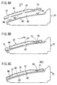
- FIG.10 shows a card terminal apparatus 50HA of the horizontal placement type in a second embodiment of the present invention.
- the card terminal apparatus 50HA in the second embodiment is similar to the above-described card terminal apparatus 50H in the first embodiment.
- the reference numerals the same as those of the first embodiment, are given for the substantially identical parts/components. Only different features will now be described.
- ends of leaf-spring terminal members 100 are fixed on the control printed substrate 55 in the first assembly 51. Terminal members 101, 102 are provided at each of the two ends of the input key and liquid crystal display panel unit 61 in the second assembly 52.
- the other ends of the leaf-spring terminal members 100 project from the second-assembly loading portion 58.
- the other ends of the leaf-spring terminal members 100 are in contact with the terminal members 101 of the second assembly 52, respectively.
- the second assembly 52 and the first assembly 51 are electrically connected with one another.
- the leaf-spring terminal members 100 and the terminal members 101 are used, it is not necessary to connect connectors before the second assembly 52 is loaded on the first assembly 51 as in the first embodiment. Merely by loading the second assembly 52 on the first assembly 51, the leaf-spring terminal members 100 are inserted into the second assembly through an opening 103 formed on the second assembly 52 and come into contact with the terminal members 101, respectively. Accordingly, the assembling work of the card terminal apparatus 50HA is easily performed in comparison to the case of the first embodiment.
- the leaf-spring terminal members 100 come into contact with the terminal members 102, respectively.
- FIG.11 shows a card terminal apparatus 50HB of the horizontal placement type in a third embodiment of the present invention.
- the card terminal apparatus 50HB in the third embodiment is similar to the above-described card terminal apparatus 50H in the first embodiment.
- the reference numerals the same as those of the first embodiment, are given for the substantially identical parts/components. Only different features will now be described.
- an infrared-ray emitting and receiving unit 110 is fixed on the control printed substrate 55 in the first assembly 51.
- an infrared-ray emitting and receiving unit 112 is fixed on the input key and liquid crystal display panel unit 61 in the second assembly 52.
- a battery 115 for supplying power to the input key and liquid crystal display panel unit 61 and to the infrared-ray emitting and receiving unit 112 is mounted on the input key and liquid crystal display panel unit 61.
- the infrared-ray emitting and receiving unit 112 faces the infrared-ray emitting and receiving unit 110.
- the second assembly 52 and the first assembly 51 are optically connected with one another. Information transmission and reception between the first assembly 51 and the second assembly 52 are performed optically through infrared rays.
- the infrared-ray emitting and receiving unit 112 faces the infrared-ray emitting and receiving unit 110.
- the second assembly 52 and the first assembly 51 are optically connected with one another.
- Information transmission and reception between the first assembly 51 and the second assembly 52 are performed optically through infrared rays.
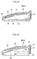
- FIG.12 shows a card terminal apparatus 50HC of the horizontal placement type in a fourth embodiment of the present invention.
- the card terminal apparatus 50HC in the fourth embodiment is similar to the above-described card terminal apparatus 50H in the first embodiment.
- the reference numerals the same as those of the first embodiment, are given for the substantially identical parts/components. Only different features will now be described.
- a radio transmitting and receiving unit 120 is fixed on the control printed substrate 55 in the first assembly 51.
- a radio transmitting and receiving unit 121 is fixed on the input key and liquid crystal display panel unit 61 in the second assembly 52.
- a battery 125 for supplying power to the input key and liquid crystal display panel unit 61 and to the radio transmitting and receiving unit 121 is mounted on the input key and liquid crystal display panel unit 61.
- the radio transmitting and receiving unit 121 faces the radio transmitting and receiving unit 120. Information transmission and reception between the first assembly 51 and the second assembly 52 are performed through radio communication.
- the radio transmitting and receiving unit 121 faces the radio transmitting and receiving unit 120. Information transmission and reception between the first assembly 51 and the second assembly 52 are performed through radio communication.
- the second assembly 52 has only input key portions. In such a case, instead of the input key and liquid crystal display panel unit 61, an input key unit which integrally has input keys is provided. Similarly, in each embodiment described above, it is also possible that the second assembly 52 has only a liquid crystal display portion. In such a case, instead of the input key and liquid crystal display panel unit 61, a liquid crystal display panel unit which integrally has a liquid crystal display panel is provided.
- FIG.13 shows a card terminal apparatus 50HD of the horizontal placement type in a fifth embodiment of the present invention.
- the card terminal apparatus 50HC in the fifth embodiment is similar to the above-described card terminal apparatus 50H in the first embodiment.
- the reference numerals the same as those of the first embodiment, are given for the substantially identical parts/components. Only different features will now be described.
- an input key, liquid crystal display panel and control printed substrate unit 130 is assembled in the second assembly 52.
- the input key, liquid crystal display panel and control printed substrate unit 130 is obtained as a result of integrating the above-described input key and liquid crystal display panel unit 61 with the control printed substrate 55.
- the input key, liquid crystal display panel and control printed substrate unit 130 is connected with the IC card reading and writing unit 54 by a cable 203 and the input key, liquid crystal display panel and control printed substrate unit 130 is connected with the external connector 201 by a cable 204.
- the cables 203 and 204 are sufficiently long that the above-mentioned connection work can be performed.
- the input key, liquid crystal display panel and control printed substrate unit 130 is connected with the IC card reading and writing unit 54 by a cable 203 and the input key, liquid crystal display panel and control printed substrate unit 130 is connected with the external connector 201 by a cable 204.
- the card terminal apparatus in the fifth embodiment because information transmission is performed without using space, reliability of signal transmission can be improved in comparison to the third and fourth embodiments. Further, in comparison to the embodiments in which the input key and liquid crystal display panel unit 61 and the control printed substrate 55 are separately provided, it is possible to reduce the manufacturing costs.
- the second assembly 52 has only the input key portions.
- an input key and control printed substrate unit which is obtained as a result of integrating the above-mentioned input key unit with the control printed substrate 55, is provided.
- the second assembly 52 has only the liquid crystal display portion.
- a liquid crystal display panel and control printed substrate unit instead of the input key, liquid crystal display panel and control printed substrate unit 130, a liquid crystal display panel and control printed substrate unit, which is obtained as a result of integrating the above-mentioned liquid crystal display panel unit with the control printed substrate 55, is provided.
- a card terminal apparatus is not necessarily limited to one for the IC card.
- the present invention can also be applied to a card terminal apparatus for a magnetic card.
Landscapes
- Engineering & Computer Science (AREA)
- Artificial Intelligence (AREA)
- Computer Vision & Pattern Recognition (AREA)
- Physics & Mathematics (AREA)
- General Physics & Mathematics (AREA)
- Theoretical Computer Science (AREA)
- Credit Cards Or The Like (AREA)
- Control Of Vending Devices And Auxiliary Devices For Vending Devices (AREA)
Applications Claiming Priority (3)
| Application Number | Priority Date | Filing Date | Title |
|---|---|---|---|
| JP15868397A JP3462365B2 (ja) | 1997-06-16 | 1997-06-16 | カード端末装置 |
| JP158683/97 | 1997-06-16 | ||
| JP15868397 | 1997-06-16 |
Publications (3)
| Publication Number | Publication Date |
|---|---|
| EP0886231A2 true EP0886231A2 (de) | 1998-12-23 |
| EP0886231A3 EP0886231A3 (de) | 2000-12-20 |
| EP0886231B1 EP0886231B1 (de) | 2004-03-31 |
Family
ID=15677088
Family Applications (1)
| Application Number | Title | Priority Date | Filing Date |
|---|---|---|---|
| EP98101189A Expired - Lifetime EP0886231B1 (de) | 1997-06-16 | 1998-01-23 | Kreditkartenterminal-Gerät |
Country Status (5)
| Country | Link |
|---|---|
| US (1) | US6085974A (de) |
| EP (1) | EP0886231B1 (de) |
| JP (1) | JP3462365B2 (de) |
| CN (1) | CN1162800C (de) |
| DE (1) | DE69822706T2 (de) |
Families Citing this family (9)
| Publication number | Priority date | Publication date | Assignee | Title |
|---|---|---|---|---|
| US6651890B2 (en) * | 1990-09-10 | 2003-11-25 | Sung Ho Byun | Combination hand-held and counter-top omnidirectional scanner |
| US6257492B1 (en) * | 1990-09-10 | 2001-07-10 | Peter Bressler | Combination hand-held and counter-top omni-directional scanner |
| JP3451035B2 (ja) | 1999-07-27 | 2003-09-29 | 日立ソフトウエアエンジニアリング株式会社 | マイクロアレイ情報表示方法 |
| TWM265663U (en) * | 2001-11-29 | 2005-05-21 | Accton Technology Corp | Vertical network apparatus |
| JP4224809B2 (ja) * | 2003-03-03 | 2009-02-18 | 旭精工株式会社 | Icカード処理装置の通信基板装着装置 |
| JP2007310736A (ja) * | 2006-05-19 | 2007-11-29 | Sanden Corp | 情報記憶媒体用リーダライタ |
| JP5082139B2 (ja) * | 2008-02-28 | 2012-11-28 | Necインフロンティア株式会社 | ブラケットをベースに実装する装置 |
| JP6691934B2 (ja) * | 2018-04-05 | 2020-05-13 | レノボ・シンガポール・プライベート・リミテッド | 連結構造体及び電子機器 |
| JP7277159B2 (ja) * | 2019-02-05 | 2023-05-18 | キヤノン株式会社 | 画像形成装置 |
Citations (2)
| Publication number | Priority date | Publication date | Assignee | Title |
|---|---|---|---|---|
| US5532466A (en) * | 1992-10-20 | 1996-07-02 | Matsushita Electric Industrial Co., Ltd. | Portable electronic equipment |
| US5608603A (en) * | 1995-05-09 | 1997-03-04 | Shin Jiuh Corp. | Computer keyboard with circuit board positioning device including positioning plates and L-shaped plug units |
Family Cites Families (4)
| Publication number | Priority date | Publication date | Assignee | Title |
|---|---|---|---|---|
| US5680633A (en) * | 1990-01-18 | 1997-10-21 | Norand Corporation | Modular, portable data processing terminal for use in a radio frequency communication network |
| US5679943A (en) * | 1989-04-28 | 1997-10-21 | Norand Corporation | Hand-held terminal with display screens, interactive screens, magnetic credit card readers, scanners, printers and handlers |
| JP3050306U (ja) | 1995-03-06 | 1998-07-14 | シーメンス ニクスドルフ インフオルマチオーンスジステーメ アクチエンゲゼルシヤフト | データ処理装置のためのモジュール式の操作ユニット |
| CA2192017C (en) | 1995-12-08 | 2000-04-25 | Masayuki Ohki | Ic card reader/writer and method of operation thereof |
-
1997
- 1997-06-16 JP JP15868397A patent/JP3462365B2/ja not_active Expired - Fee Related
-
1998
- 1998-01-21 US US09/009,926 patent/US6085974A/en not_active Expired - Lifetime
- 1998-01-23 DE DE69822706T patent/DE69822706T2/de not_active Expired - Lifetime
- 1998-01-23 EP EP98101189A patent/EP0886231B1/de not_active Expired - Lifetime
- 1998-02-05 CN CNB981043720A patent/CN1162800C/zh not_active Expired - Fee Related
Patent Citations (2)
| Publication number | Priority date | Publication date | Assignee | Title |
|---|---|---|---|---|
| US5532466A (en) * | 1992-10-20 | 1996-07-02 | Matsushita Electric Industrial Co., Ltd. | Portable electronic equipment |
| US5608603A (en) * | 1995-05-09 | 1997-03-04 | Shin Jiuh Corp. | Computer keyboard with circuit board positioning device including positioning plates and L-shaped plug units |
Also Published As
| Publication number | Publication date |
|---|---|
| EP0886231B1 (de) | 2004-03-31 |
| DE69822706D1 (de) | 2004-05-06 |
| CN1162800C (zh) | 2004-08-18 |
| CN1202668A (zh) | 1998-12-23 |
| JPH117508A (ja) | 1999-01-12 |
| DE69822706T2 (de) | 2005-02-10 |
| US6085974A (en) | 2000-07-11 |
| JP3462365B2 (ja) | 2003-11-05 |
| EP0886231A3 (de) | 2000-12-20 |
Similar Documents
| Publication | Publication Date | Title |
|---|---|---|
| US6244894B1 (en) | Cellular phone battery equipped with IC card | |
| US6808424B2 (en) | Memory card installer | |
| US6602096B1 (en) | Card-receiving device for a communication apparatus | |
| JP3530460B2 (ja) | カードコネクタ | |
| US6304416B1 (en) | Two axis reading of memory chip in cartridge | |
| JP2001274567A (ja) | 取り外し可能な構成要素のための電気的コネクタ | |
| US5477213A (en) | Data input device for IC-key lock system | |
| US5739515A (en) | IC card reader/writer | |
| US20030081375A1 (en) | Portable information terminal capable of sliding one case unit against another case unit in the use state | |
| US7789691B2 (en) | Chip card retaining mechanism and printed circuit board module incorporating same | |
| EP0886231B1 (de) | Kreditkartenterminal-Gerät | |
| US6942153B1 (en) | Handheld computer | |
| US6839229B2 (en) | Information processing device and external unit | |
| US6434010B1 (en) | IC card assembly | |
| EP1326194A2 (de) | Elektronische Vorrichtung mit einer Halterung, die mit einer SD-Karte geladen werden kann | |
| US7813136B2 (en) | Server enclosure | |
| EP1050840A2 (de) | Verbesserter , über einer Leiterplatte angeordneter IC-Kartenleser | |
| EP1045337B1 (de) | Chipkarte mit einer Antenne | |
| EP1085606B1 (de) | Chipkartenleser-Vorrichtung | |
| US7389924B2 (en) | Electronic card connector | |
| US5086336A (en) | Semiconductor device card | |
| US20080090611A1 (en) | System and Method for Information Handling System Modular Wireless Integration | |
| CN217720126U (zh) | 存储卡连接端口模块 | |
| CN212163467U (zh) | 主板和手持终端 | |
| EP1058203B1 (de) | Tragbares Endgerät für ein Informationsverarbeitungssystem |
Legal Events
| Date | Code | Title | Description |
|---|---|---|---|
| PUAI | Public reference made under article 153(3) epc to a published international application that has entered the european phase |
Free format text: ORIGINAL CODE: 0009012 |
|
| AK | Designated contracting states |
Kind code of ref document: A2 Designated state(s): DE FR GB |
|
| AX | Request for extension of the european patent |
Free format text: AL;LT;LV;MK;RO;SI |
|
| PUAL | Search report despatched |
Free format text: ORIGINAL CODE: 0009013 |
|
| AK | Designated contracting states |
Kind code of ref document: A3 Designated state(s): AT BE CH DE DK ES FI FR GB GR IE IT LI LU MC NL PT SE |
|
| AX | Request for extension of the european patent |
Free format text: AL;LT;LV;MK;RO;SI |
|
| 17P | Request for examination filed |
Effective date: 20010123 |
|
| AKX | Designation fees paid |
Free format text: DE FR GB |
|
| GRAP | Despatch of communication of intention to grant a patent |
Free format text: ORIGINAL CODE: EPIDOSNIGR1 |
|
| GRAS | Grant fee paid |
Free format text: ORIGINAL CODE: EPIDOSNIGR3 |
|
| GRAA | (expected) grant |
Free format text: ORIGINAL CODE: 0009210 |
|
| AK | Designated contracting states |
Kind code of ref document: B1 Designated state(s): DE FR GB |
|
| REG | Reference to a national code |
Ref country code: GB Ref legal event code: FG4D |
|
| REF | Corresponds to: |
Ref document number: 69822706 Country of ref document: DE Date of ref document: 20040506 Kind code of ref document: P |
|
| ET | Fr: translation filed | ||
| PLBE | No opposition filed within time limit |
Free format text: ORIGINAL CODE: 0009261 |
|
| STAA | Information on the status of an ep patent application or granted ep patent |
Free format text: STATUS: NO OPPOSITION FILED WITHIN TIME LIMIT |
|
| 26N | No opposition filed |
Effective date: 20050104 |
|
| PGFP | Annual fee paid to national office [announced via postgrant information from national office to epo] |
Ref country code: FR Payment date: 20130204 Year of fee payment: 16 Ref country code: DE Payment date: 20130116 Year of fee payment: 16 Ref country code: GB Payment date: 20130123 Year of fee payment: 16 |
|
| REG | Reference to a national code |
Ref country code: DE Ref legal event code: R119 Ref document number: 69822706 Country of ref document: DE |
|
| GBPC | Gb: european patent ceased through non-payment of renewal fee |
Effective date: 20140123 |
|
| REG | Reference to a national code |
Ref country code: DE Ref legal event code: R119 Ref document number: 69822706 Country of ref document: DE Effective date: 20140801 |
|
| PG25 | Lapsed in a contracting state [announced via postgrant information from national office to epo] |
Ref country code: DE Free format text: LAPSE BECAUSE OF NON-PAYMENT OF DUE FEES Effective date: 20140801 |
|
| REG | Reference to a national code |
Ref country code: FR Ref legal event code: ST Effective date: 20140930 |
|
| PG25 | Lapsed in a contracting state [announced via postgrant information from national office to epo] |
Ref country code: GB Free format text: LAPSE BECAUSE OF NON-PAYMENT OF DUE FEES Effective date: 20140123 Ref country code: FR Free format text: LAPSE BECAUSE OF NON-PAYMENT OF DUE FEES Effective date: 20140131 |