EP0886218B1 - Time multiplexed scheme for deadlock resolution in distributed arbitration - Google Patents
Time multiplexed scheme for deadlock resolution in distributed arbitration Download PDFInfo
- Publication number
- EP0886218B1 EP0886218B1 EP98300659A EP98300659A EP0886218B1 EP 0886218 B1 EP0886218 B1 EP 0886218B1 EP 98300659 A EP98300659 A EP 98300659A EP 98300659 A EP98300659 A EP 98300659A EP 0886218 B1 EP0886218 B1 EP 0886218B1
- Authority
- EP
- European Patent Office
- Prior art keywords
- bus
- access
- arbiter
- free
- granting
- Prior art date
- Legal status (The legal status is an assumption and is not a legal conclusion. Google has not performed a legal analysis and makes no representation as to the accuracy of the status listed.)
- Expired - Lifetime
Links
Images


Classifications
-
- G—PHYSICS
- G06—COMPUTING OR CALCULATING; COUNTING
- G06F—ELECTRIC DIGITAL DATA PROCESSING
- G06F13/00—Interconnection of, or transfer of information or other signals between, memories, input/output devices or central processing units
- G06F13/14—Handling requests for interconnection or transfer
- G06F13/36—Handling requests for interconnection or transfer for access to common bus or bus system
- G06F13/362—Handling requests for interconnection or transfer for access to common bus or bus system with centralised access control
- G06F13/364—Handling requests for interconnection or transfer for access to common bus or bus system with centralised access control using independent requests or grants, e.g. using separated request and grant lines
Definitions
- This invention relates to arbitration and more particularly to bus arbitration between a network interface and a host computer sending and receiving data to and from the network interface to avoid bus contention problems.
- Modern computer systems often include controllers, processors, memories and peripheral devices. Data is often required to be transmitted over buses connecting these components.
- An example of such a system is a local area network which includes a number of network stations.
- the network station typically includes a Media Access Control (MAC) layer network interface that sends and receives data to a host processor via a peripheral component interconnect (PCI) interface.
- MAC Media Access Control
- PCI peripheral component interconnect
- Some network interfaces include an expansion bus interface for buffering data between the PCI interface and the MAC transmit and receive FIFOs. Specifically, this interface may be used to access a shared external memory device for storing additional transmit and receive data.
- attempts to access the expansion bus interface for storage or retrieval of transmit data or receive data may occur independently. Hence, attempts to access the same resource at the same time results in bus contention problems or bus deadlock problems since two independent activities are attempting to access the same resource via the same bus.
- a first and second arbiter grant access requests to a first bus or a second bus during respective exclusive portions of a clock signal.
- a system for arbitrating bus access requests includes a first and second arbiter.
- the first arbiter grants access, to a first requesting agent, to a first bus during a first portion of a clock signal and based on an availability of a second bus.
- the second arbiter grants access, to a second requesting agent, to a second bus during a second portion of the clock signal and based on an availability of the second bus, where the first requesting agent requires access to the first and second buses.
- the granting of access by the first and second arbiters during respective portions of the clock signal ensures that the arbiters do not reach a deadlock or a contention case when attempting to grant access to a shared resource.
- use of different clock signal portions enables reliable arbitration with minimal logic.
- EP 0 774 717 discloses a generic Input/Output interface between an IO block and a System and ATM Layer Core on a network interface circuit is provided.
- the GIO interface includes parallel DM read and write control handshake signal lines; parallel DMA read and write data handshake signal lines which operate independently from the read and write control handshake signal lines; parallel DM read and write data signal lines, and a single clock signal line.
- the present invention provides an arbitration system comprising a first arbiter configured for granting, to a first requesting agent, access to a first bus (A) during a first portion of a clock signal and based on an availability of a second bus (S); and a second arbiter configured for granting, to a second requesting agent, access to the second bus (S) during a second portion of the clock signal and based on an availability of the second bus (S), the first requesting agent requiring concurrent access to the first and second buses.
- FIG. 1 is a block diagram of an exemplary system in a network station which uses the arbitration scheme of the invention. It will become apparent, however, that the present invention is also applicable to any other system which requires resource arbitration.
- Figure 1 includes a data controller 10 that controls data transfers between a network interface and a host controller in a network station.
- the system includes a peripheral component interconnect (PCI) interface 12 that supports communication between a PCI bus and data controller 10 via a first data bus, referred to as the "A bus”.
- a media access control (MAC) network interface 16 transfers data between the data controller 10 via a second data bus referred to as the "M bus”.
- the MAC network interface 16 outputs data packets onto a network, for example an Ethernet (IEEE 802.3) network, carrying data supplied from the data controller 10.
- the system also includes an external memory 14, preferably implemented as a static RAM (SRAM), that transfers data between the data controller 10 via a data bus referred to as the "S bus".
- the external memory 14 provides for the temporary storage of data being transferred between the host controller and connected workstations via the network, and supplements internal buffers within the PCI interface 12 and the MAC 16.
- FIG. 2 is a data flow diagram illustrating four agents executed by the data controller 10.
- the agents include a transmit direct memory access (Tx DMA) agent 26, receive direct memory access (Rx DMA) agent 28, transmit MAC (Tx MAC) agent 30 and receive MAC (Rx MAC) agent 32.
- the agents may be implemented, for example, as logic state machines.
- the agents 26 and 30 control the transfer of data (i.e., data flow) from the PCI interface 12 to the MAC 16 via SRAM 14 (i.e., the transmit data path), and the agents 28 and 32 control the transfer of data from the MAC 16 to the PCI interface 12 (i.e., the receive path).
- the transmit and receive data paths share SRAM 14.
- the data controller 10 provides a mechanism for the four contending agents to access SRAM 14.
- the transmit DMA agent 26 coordinates all the activities for moving frames from the PCI interface 12 to the SRAM 14. These activities include descriptor read, data transfer from PCI bus to SRAM 14, status writes, and all the initialization needed by the above DMA activities.
- the Tx DMA agent 26 moves frames from the PCI interface input FIFO 18 to SRAM 14 via the A bus and the S bus.
- the Tx MAC agent 30 moves data to the MAC transmit FIFO 22 via the S bus.
- transmit MAC agent 30 detects a ready condition of MAC transmit FIFO 22
- transmit MAC agent 30 checks for a complete transmit frame in SRAM 14, and asserts a request signal to an arbiter, described below.
- the transmit MAC agent 30 may check if the transmit FIFO storage capacity reaches a prescribed threshold. After receiving a grant signal from the arbiter, the transmit MAC agent 30 calls a low level module to perform a data transfer of up to eight words to the MAC transmit FIFO 22.
- the receive MAC agent 32 moves frames from MAC receive FIFO 24 to the SRAM 14 via the S bus.
- the SRAM 14 includes a queue scheme configured to hold as much as 64 frames without causing a receive overflow.
- a 64x32 bit long queue holds the frame length and receive status information for each normal frame received from MAC 16.
- the receive MAC agent 32 first checks to see if any exceptional condition exists which may cause a receive frame discard and a receive FIFO flush. If there is such a condition, the receive MAC agent 32 flushes the SRAM 14. When data is available from the receive FIFO 24, the receive MAC agent 32 sends a request to the arbiter and waits for the grant. The receive MAC agent 32 subsequently calls a low level module to perform a transfer of up to eight words from MAC receive FIFO 24 to the SRAM 14.
- the receive DMA agent 28 coordinates all the activities for moving frames from SRAM 14 to the PCI bus. These activities include descriptor read, data transfer from SRAM 14 to PCI bus, status writes, and all the initialization needed by the above DMA activities.
- a descriptor controller is included in data controller 10.
- the descriptor controller activities include receive status write (Rx Stat Wr), transmit status write (Tx Stat Wr), receive descriptor read (Rx Desc Rd) and transmit descriptor read (Tx Desc Rd).
- a slave controller is also included in data controller 10 and activities of the slave controller include slave read/write (Slv RW). All of these activities of the descriptor controller and slave controller require access to the A bus.
- FIG. 3 is a block diagram illustrating the data controller 10 according to an embodiment of the present invention.
- the data controller 10 includes executable agents for performing specified operations.
- a first group of agents (26, 28, 30 and 32) share access to the SRAM 14, and hence must share access to the S bus.
- DMA agents 26 and 28 also require concurrent (i.e., simultaneous) access to both the A bus and the S bus for transfers between the PCI interface 12 and the SRAM 14.
- a second group of agents (Slv RW 34, Rx Stat Wr 36, Tx Stat Wr 38, Rx Desc Rd 40 and Tx Desc Rd 42) share access to the A bus.
- the data controller 10 includes arbiter S 44 and arbiter A 46 that control access for bus S and bus A, respectively.
- the arbiters 44 and 46 perform arbitration using request (REQ) and grant (GNT) hand-shaking signals, a bus free signal, and a clock signal.
- transmit MAC request is a request generated by transmit MAC agent 30 to arbiter S 44 for access to S bus.
- Arbiter S 44 receives this request and grants access to the transmit MAC agent 30 by sending a transmit MAC grant (TX MAC GNT) signal to the transmit MAC agent 30.
- TX MAC GNT transmit MAC grant
- the other access requests to arbiters S 44 and A 46, respectively, are performed in the same manner. Only one agent can be granted access to a shared resource (e.g., the A bus) at any given time.
- transmit DMA 26 and receive DMA 28 transfer data between the PCI bus and SRAM 14, requiring access to the A bus and the S bus simultaneously.
- arbiter A 46 and arbiter S 44 communicate the status of their respective buses with signals A FREE and S FREE.
- Arbiter A 46 generates and sends signal A FREE to arbiter S 44 when A bus is available. Similarly, arbiter S 44 generates and sends S FREE to arbiter A 46. Signal S FREE is normally asserted, but is de-asserted when arbiter S 44 intends to give a grant to either transmit DMA agent 26 or receive DMA agent 28 for accessing both the S bus and the A bus. Hence, S FREE is deasserted only when both the S bus and A bus are unavailable. Signal A FREE is normally asserted, but is de-asserted when arbiter A 46 intends to give a grant to any one of the agents in the second group.
- a grant will not be given to transmit DMA agent 26 or receive DMA agent 28 by arbiter S 44 unless A FREE is asserted, due to the fact that these two agents require access to the A bus as well as the S bus. Similarly, a grant will not be given to one of the agents in the second group by arbiter A 46 unless S FREE is asserted.
- Figure 4 illustrates a potential problem that may occur in the arbitration scheme of Figure 3 when the arbitration arrangement of the present invention is not used.
- REQ S represents a request generated by transmit DMA agent 26 or receive DMA agent 28 requiring access to the S and A buses
- REQ A represents a request generated by one of the agents from the second group (e.g., agents 34, 36, 38, 40 or 42) requiring access to the A bus.
- GNT S represents only one grant to either transmit DMA agent 26 or receive DMA agent 28, while GNT A represents only one grant to one of the agents from the second group.
- arbiter S 44 deasserts S FREE at event 66 to inform arbiter A 46 at the second clock that S bus is no longer available.
- GNT S is asserted if A FREE is asserted.
- Arbiter A 46 operates the same way at the same time upon REQ A. That is, arbiter A 46 responds to REQ A at event 60 by de-asserting A FREE at event 64 to inform arbiter S 44 at the second clock that S bus and A bus are no longer available.
- GNT A is asserted if S FREE is asserted.
- a deadlock occurs at the third clock cycle because each arbiter, 44 and 46, thinks that the shared A bus is busy and neither of the grant signals are asserted at events 68 and 69.
- the agent requesting access to the A bus is denied access and the agent requesting access to the S bus is also denied access.
- Figure 5 illustrates another potential problem that may occur in the arbitration scheme of Figure 3 when the arbitration arrangement of the present invention is not used.
- arbiter S 44 informs arbiter A 46 that S bus and A bus are not available at the second clock by de-asserting S FREE at event 86 and asserting GNT S at event 89 to grant access to S bus and A bus.
- Arbiter A 46 responds to REQ A at event 80 by informing arbiter S 44 that A bus is not available at the second clock by de-asserting A FREE at event 84 and asserting GNT A at event 88 to grant access to A bus.
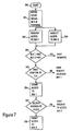
- FIG. 7 is a flow diagram illustrating the method for arbitrating access according to an embodiment of the present invention.
- the disclosed method may be implemented in parallel (e.g., as a state machine).
- the data controller 10 generates a PHASE signal as a divided- by-two clock derived from the system clock, CLK.
- the high phase at 101, 103, 105, 107 and 109 (PHA) is reserved as a first exclusive portion of the system clock signal for arbiter A 46 while the low phase at 100, 102, 104, 106, 108 and 110 (PHS) is reserved as a second exclusive portion for arbiter S 44.
- the system clock, CLK in the exemplary system is a 33 MHz crystal reference clock. However, any known reference signal providing a stable clock signal may be used. In addition, the details of generating a divided by two clock derived from a reference clock are not needed for the present invention. Any typical device known in the art to receive an input clock signal and generate a new clock signal which is a divided by two version of the reference clock is suitable for use in the invention.
- arbiter A 46 de-asserts A FREE and asserts GNT A only during the corresponding exclusive portion PHA in response to REQ A in step 202 and arbiter S 44 de-asserts S FREE and asserts GNT S only during the corresponding exclusive portion PHS in response to REQ S in step 203.
- S FREE and A FREE must be asserted (i.e., A bus must be free) for either request to be granted regardless of which phase the clock is in. Since arbiter A 46 and arbiter S 44 never make a decision at the same phase, the deadlock and contention cases are avoided.
- arbiter A 46 checks in step 204 if both S FREE and A FREE are asserted, and asserts GNT A at event 124 during the exclusive portion PHA in steps 205 and 206 and de-asserts A FREE at event 118. Therefore, access to A bus is granted to an agent in the second group (e.g., agent 34, 36, 38, 40, or 42) requesting access to the A bus. During this time, arbiter S denies requests in step 204. When REQ A is de-asserted at event 114, A FREE is re-asserted at event 120.
- the time multiplexed arbitration system described in the exemplary embodiment uses two arbiters and divides the clock signal into two phases, one for each arbiter.
- the multiplexed arbitration system is equally applicable to systems which include more than two arbiters.
- a system may utilize three arbiters for arbitrating access to three separate buses.
- the clock signal is divided into three phases, one phase for each arbiter.
- the first phase is utilized for granting access to the first activity, the second phase for the second activity and the third phase for the third activity.
- the clock is divided into four phases.
- the exemplary embodiment of the time multiplexed arbitration system also assumes that the clock phases are of equal duration.
- the invention may assign different portions of the clock cycle, or time slices, to different arbiters. For example, if it is known that a first activity occurs more frequently than a second activity, the first portion of the clock cycle may be longer in duration than a second portion of the clock cycle. In this manner, the request from a first activity is more likely to be granted at any given time since the period of time that the first arbiter may grant the request is longer than the period of time that the second arbiter may grant the request.
- the exemplary embodiment of the invention also shows the buses being located external to the chip.
- the invention is usable in a system in which the buses are internal buses within the chip.
- the disclosed arrangement is applicable to systems using multiple arbiters sharing multiple buses. Hence, different variations of arbiters and buses may be used.
- An advantage of the invention is that the arbitration scheme enables the system to process data transfers in a timely manner without requiring complex arbitration algorithms to determine how to transfer the data.
- Another advantage of the invention is that the arbitration scheme used does not require a hierarchy of arbiters to resolve resource contention. This saves processing time and enables the arbiters to save chip space by eliminating complex logic.
- the disclosed embodiment is applicable to interface devices and bus arbitration controllers in networked computers and network control systems.
Landscapes
- Engineering & Computer Science (AREA)
- Theoretical Computer Science (AREA)
- Physics & Mathematics (AREA)
- General Engineering & Computer Science (AREA)
- General Physics & Mathematics (AREA)
- Bus Control (AREA)
Applications Claiming Priority (2)
| Application Number | Priority Date | Filing Date | Title |
|---|---|---|---|
| US879202 | 1997-06-19 | ||
| US08/879,202 US6061361A (en) | 1997-06-19 | 1997-06-19 | Time multiplexed scheme for deadlock resolution in distributed arbitration |
Publications (3)
| Publication Number | Publication Date |
|---|---|
| EP0886218A2 EP0886218A2 (en) | 1998-12-23 |
| EP0886218A3 EP0886218A3 (en) | 2003-04-09 |
| EP0886218B1 true EP0886218B1 (en) | 2004-12-01 |
Family
ID=25373631
Family Applications (1)
| Application Number | Title | Priority Date | Filing Date |
|---|---|---|---|
| EP98300659A Expired - Lifetime EP0886218B1 (en) | 1997-06-19 | 1998-01-29 | Time multiplexed scheme for deadlock resolution in distributed arbitration |
Country Status (4)
| Country | Link |
|---|---|
| US (1) | US6061361A (enExample) |
| EP (1) | EP0886218B1 (enExample) |
| JP (1) | JP4625549B2 (enExample) |
| DE (1) | DE69827879T2 (enExample) |
Families Citing this family (7)
| Publication number | Priority date | Publication date | Assignee | Title |
|---|---|---|---|---|
| US6738845B1 (en) | 1999-11-05 | 2004-05-18 | Analog Devices, Inc. | Bus architecture and shared bus arbitration method for a communication device |
| DE19961124A1 (de) * | 1999-12-17 | 2001-06-21 | Infineon Technologies Ag | Schnittstelle |
| US6778548B1 (en) * | 2000-06-26 | 2004-08-17 | Intel Corporation | Device to receive, buffer, and transmit packets of data in a packet switching network |
| US7035277B1 (en) * | 2000-08-31 | 2006-04-25 | Cisco Technology, Inc. | Priority-based arbitration system for context switching applications |
| EP1989695B1 (en) | 2006-02-20 | 2013-04-24 | Robert Bosch GmbH | Obstruction detection device |
| FR3087982B1 (fr) | 2018-10-31 | 2020-12-04 | Commissariat Energie Atomique | Procede et circuit de multiplexage temporel d'acces concurrents a une ressource informatique |
| TWI739556B (zh) * | 2020-08-19 | 2021-09-11 | 瑞昱半導體股份有限公司 | 時脈死結檢測系統、方法以及非暫態電腦可讀取媒體 |
Family Cites Families (6)
| Publication number | Priority date | Publication date | Assignee | Title |
|---|---|---|---|---|
| IT1229667B (it) * | 1989-04-24 | 1991-09-06 | Bull Hn Information Syst | Sistema di elaborazione dati con arbitratore duale di accesso a bus di sistema. |
| JP3464799B2 (ja) * | 1993-03-12 | 2003-11-10 | モトローラ・インコーポレーテッド | パケット伝送システムにおける競合および資源の不適当な割当ての可能性を低減する方法および装置 |
| US5713025A (en) * | 1993-10-21 | 1998-01-27 | Sun Microsystems, Inc. | Asynchronous arbiter using multiple arbiter elements to enhance speed |
| US5787265A (en) * | 1995-09-28 | 1998-07-28 | Emc Corporation | Bus arbitration system having a pair of logic networks to control data transfer between a memory and a pair of buses |
| US5745684A (en) * | 1995-11-06 | 1998-04-28 | Sun Microsystems, Inc. | Apparatus and method for providing a generic interface between a host system and an asynchronous transfer mode core functional block |
| US5797018A (en) * | 1995-12-07 | 1998-08-18 | Compaq Computer Corporation | Apparatus and method of preventing a deadlock condition in a computer system |
-
1997
- 1997-06-19 US US08/879,202 patent/US6061361A/en not_active Expired - Lifetime
-
1998
- 1998-01-29 DE DE69827879T patent/DE69827879T2/de not_active Expired - Lifetime
- 1998-01-29 EP EP98300659A patent/EP0886218B1/en not_active Expired - Lifetime
- 1998-02-18 JP JP03565898A patent/JP4625549B2/ja not_active Expired - Fee Related
Also Published As
| Publication number | Publication date |
|---|---|
| JPH1125036A (ja) | 1999-01-29 |
| US6061361A (en) | 2000-05-09 |
| EP0886218A3 (en) | 2003-04-09 |
| DE69827879T2 (de) | 2005-11-03 |
| EP0886218A2 (en) | 1998-12-23 |
| DE69827879D1 (de) | 2005-01-05 |
| JP4625549B2 (ja) | 2011-02-02 |
Similar Documents
| Publication | Publication Date | Title |
|---|---|---|
| US6151651A (en) | Communication link with isochronous and asynchronous priority modes coupling bridge circuits in a computer system | |
| US6393506B1 (en) | Virtual channel bus and system architecture | |
| US6148357A (en) | Integrated CPU and memory controller utilizing a communication link having isochronous and asynchronous priority modes | |
| US5933610A (en) | Predictive arbitration system for PCI bus agents | |
| EP0581335B1 (en) | Data processing system having units competing for access to shared resources and arbitration unit responsive to the status of the shared resources | |
| CA2036688C (en) | Multiple cluster signal processor | |
| US5119480A (en) | Bus master interface circuit with transparent preemption of a data transfer operation | |
| US5710891A (en) | Pipelined distributed bus arbitration system | |
| US5546547A (en) | Memory bus arbiter for a computer system having a dsp co-processor | |
| US6519666B1 (en) | Arbitration scheme for optimal performance | |
| US5515523A (en) | Method and apparatus for arbitrating conflicts by monitoring number of access requests per unit of time in multiport memory systems | |
| US5590299A (en) | Multiprocessor system bus protocol for optimized accessing of interleaved storage modules | |
| US6134625A (en) | Method and apparatus for providing arbitration between multiple data streams | |
| US6425037B1 (en) | Information processing system, bus arbiter, and bus controlling method | |
| US7124232B2 (en) | Bus connection circuit and bus connection system having plural request queues, a bus interface portion outputting request signals, an arbiter performing arbitration of plural requests and a bus interface portion outputting a request signal indicating allocation of pre-fetch buffers corresponding to arbitrated requests | |
| GB2228349A (en) | Data transfer bus with virtual memory | |
| KR100708096B1 (ko) | 버스 시스템 및 그 실행 순서 조정방법 | |
| EP0886218B1 (en) | Time multiplexed scheme for deadlock resolution in distributed arbitration | |
| US6199132B1 (en) | Communication link with isochronous and asynchronous priority modes | |
| EP1096387B1 (en) | An arbitration unit for a bus | |
| US6247089B1 (en) | Efficient data loading scheme to minimize PCI bus arbitrations delays and wait states | |
| US8176304B2 (en) | Mechanism for performing function level reset in an I/O device | |
| EP1811394B1 (en) | An arbitrator and its arbitration method | |
| US6105082A (en) | Data processor used in a data transfer system which includes a detection circuit for detecting whether processor uses bus in a forthcoming cycle | |
| JP4097847B2 (ja) | バス・ブリッジのアービトレーション方法 |
Legal Events
| Date | Code | Title | Description |
|---|---|---|---|
| PUAI | Public reference made under article 153(3) epc to a published international application that has entered the european phase |
Free format text: ORIGINAL CODE: 0009012 |
|
| AK | Designated contracting states |
Kind code of ref document: A2 Designated state(s): AT BE CH DE DK ES FI FR GB GR IE IT LI LU MC NL PT SE |
|
| AX | Request for extension of the european patent |
Free format text: AL;LT;LV;MK;RO;SI |
|
| PUAL | Search report despatched |
Free format text: ORIGINAL CODE: 0009013 |
|
| AK | Designated contracting states |
Kind code of ref document: A3 Designated state(s): AT BE CH DE DK ES FI FR GB GR IE IT LI LU MC NL PT SE |
|
| AX | Request for extension of the european patent |
Extension state: AL LT LV MK RO SI |
|
| RIC1 | Information provided on ipc code assigned before grant |
Ipc: 7G 06F 13/12 B Ipc: 7G 06F 13/40 B Ipc: 7G 06F 13/364 A |
|
| 17P | Request for examination filed |
Effective date: 20030519 |
|
| 17Q | First examination report despatched |
Effective date: 20030828 |
|
| AKX | Designation fees paid |
Designated state(s): DE FR GB IE IT |
|
| GRAP | Despatch of communication of intention to grant a patent |
Free format text: ORIGINAL CODE: EPIDOSNIGR1 |
|
| GRAS | Grant fee paid |
Free format text: ORIGINAL CODE: EPIDOSNIGR3 |
|
| GRAA | (expected) grant |
Free format text: ORIGINAL CODE: 0009210 |
|
| AK | Designated contracting states |
Kind code of ref document: B1 Designated state(s): DE FR GB IE IT |
|
| PG25 | Lapsed in a contracting state [announced via postgrant information from national office to epo] |
Ref country code: IT Free format text: LAPSE BECAUSE OF FAILURE TO SUBMIT A TRANSLATION OF THE DESCRIPTION OR TO PAY THE FEE WITHIN THE PRE;WARNING: LAPSES OF ITALIAN PATENTS WITH EFFECTIVE DATE BEFORE 2007 MAY HAVE OCCURRED AT ANY TIME BEFORE 2007. THE CORRECT EFFECTIVE DATE MAY BE DIFFERENT FROM THE ONE RECORDED.SCRIBED TIME-LIMIT Effective date: 20041201 |
|
| REG | Reference to a national code |
Ref country code: GB Ref legal event code: FG4D |
|
| REG | Reference to a national code |
Ref country code: IE Ref legal event code: FG4D |
|
| REF | Corresponds to: |
Ref document number: 69827879 Country of ref document: DE Date of ref document: 20050105 Kind code of ref document: P |
|
| PG25 | Lapsed in a contracting state [announced via postgrant information from national office to epo] |
Ref country code: IE Free format text: LAPSE BECAUSE OF NON-PAYMENT OF DUE FEES Effective date: 20050131 |
|
| PLBE | No opposition filed within time limit |
Free format text: ORIGINAL CODE: 0009261 |
|
| STAA | Information on the status of an ep patent application or granted ep patent |
Free format text: STATUS: NO OPPOSITION FILED WITHIN TIME LIMIT |
|
| REG | Reference to a national code |
Ref country code: IE Ref legal event code: MM4A |
|
| 26N | No opposition filed |
Effective date: 20050902 |
|
| ET | Fr: translation filed | ||
| REG | Reference to a national code |
Ref country code: GB Ref legal event code: 732E Free format text: REGISTERED BETWEEN 20091210 AND 20091216 |
|
| REG | Reference to a national code |
Ref country code: FR Ref legal event code: TP |
|
| PGFP | Annual fee paid to national office [announced via postgrant information from national office to epo] |
Ref country code: FR Payment date: 20101221 Year of fee payment: 14 |
|
| PGFP | Annual fee paid to national office [announced via postgrant information from national office to epo] |
Ref country code: GB Payment date: 20101215 Year of fee payment: 14 |
|
| PGFP | Annual fee paid to national office [announced via postgrant information from national office to epo] |
Ref country code: DE Payment date: 20110131 Year of fee payment: 14 |
|
| GBPC | Gb: european patent ceased through non-payment of renewal fee |
Effective date: 20120129 |
|
| REG | Reference to a national code |
Ref country code: FR Ref legal event code: ST Effective date: 20120928 |
|
| PG25 | Lapsed in a contracting state [announced via postgrant information from national office to epo] |
Ref country code: DE Free format text: LAPSE BECAUSE OF NON-PAYMENT OF DUE FEES Effective date: 20120801 Ref country code: GB Free format text: LAPSE BECAUSE OF NON-PAYMENT OF DUE FEES Effective date: 20120129 |
|
| REG | Reference to a national code |
Ref country code: DE Ref legal event code: R119 Ref document number: 69827879 Country of ref document: DE Effective date: 20120801 |
|
| PG25 | Lapsed in a contracting state [announced via postgrant information from national office to epo] |
Ref country code: FR Free format text: LAPSE BECAUSE OF NON-PAYMENT OF DUE FEES Effective date: 20120131 |