EP0884683A2 - Cache device - Google Patents
Cache device Download PDFInfo
- Publication number
- EP0884683A2 EP0884683A2 EP98250210A EP98250210A EP0884683A2 EP 0884683 A2 EP0884683 A2 EP 0884683A2 EP 98250210 A EP98250210 A EP 98250210A EP 98250210 A EP98250210 A EP 98250210A EP 0884683 A2 EP0884683 A2 EP 0884683A2
- Authority
- EP
- European Patent Office
- Prior art keywords
- data
- main memory
- cache
- block
- cache device
- Prior art date
- Legal status (The legal status is an assumption and is not a legal conclusion. Google has not performed a legal analysis and makes no representation as to the accuracy of the status listed.)
- Granted
Links
Images


Classifications
-
- G—PHYSICS
- G06—COMPUTING; CALCULATING OR COUNTING
- G06F—ELECTRIC DIGITAL DATA PROCESSING
- G06F12/00—Accessing, addressing or allocating within memory systems or architectures
- G06F12/02—Addressing or allocation; Relocation
- G06F12/08—Addressing or allocation; Relocation in hierarchically structured memory systems, e.g. virtual memory systems
- G06F12/0802—Addressing of a memory level in which the access to the desired data or data block requires associative addressing means, e.g. caches
- G06F12/0888—Addressing of a memory level in which the access to the desired data or data block requires associative addressing means, e.g. caches using selective caching, e.g. bypass
-
- G—PHYSICS
- G06—COMPUTING; CALCULATING OR COUNTING
- G06F—ELECTRIC DIGITAL DATA PROCESSING
- G06F12/00—Accessing, addressing or allocating within memory systems or architectures
- G06F12/02—Addressing or allocation; Relocation
- G06F12/08—Addressing or allocation; Relocation in hierarchically structured memory systems, e.g. virtual memory systems
- G06F12/0802—Addressing of a memory level in which the access to the desired data or data block requires associative addressing means, e.g. caches
- G06F12/0844—Multiple simultaneous or quasi-simultaneous cache accessing
- G06F12/0855—Overlapped cache accessing, e.g. pipeline
- G06F12/0859—Overlapped cache accessing, e.g. pipeline with reload from main memory
-
- G—PHYSICS
- G06—COMPUTING; CALCULATING OR COUNTING
- G06F—ELECTRIC DIGITAL DATA PROCESSING
- G06F9/00—Arrangements for program control, e.g. control units
- G06F9/06—Arrangements for program control, e.g. control units using stored programs, i.e. using an internal store of processing equipment to receive or retain programs
- G06F9/30—Arrangements for executing machine instructions, e.g. instruction decode
- G06F9/38—Concurrent instruction execution, e.g. pipeline, look ahead
- G06F9/3824—Operand accessing
Definitions
- This invention relates to a cache device, particularly to a cache device connected between at least one processing unit and a main memory shared by a plurality of the processing units.
- a conventional cache device when a load request to a main memory results in a cache miss, block data including the data indicated by the load request is fetched to the main memory. The block data returned from the main memory are written into the cache memory, and at the same time the desired data is so treated as to be sent back to a processing unit which issues the load request.
- the device is provided with a non-blocking hardware mechanism by virtue of which the cache can manage, even when a cache miss occurs, subsequent load requests up to two requests.
- a conventional information processing system to increase its information processing capacity, is so constructed as to have its main memory shared by a plurality of processors, and with such system it often occurs that load requests from different processors must be handled at the same time.
- load requests from different processors must be handled at the same time.
- block load data moved from the main memory to the processor are not sent back in a sequential order, but haphazardly with the intervals between adjacent block data being made inconstant.
- block load data are handled by smaller basic data units.
- an identical path acts at the same time as a reply data path through which target data contained in the block data delivered by the main memory is returned to a general purpose register, and as a read path through which, when the cache contains the target data, that is, when a cache hit occurs, the required target data is read from the cache.
- the cache device returns the target data contained in the block load data delivered by the main memory to the processing unit which issued the load request, data from a data array become impossible because the involved path therefor has been taken over in competition.
- subsequent instructions to load data into the main memory are inhibited from accessing to the cache, and hence handling of subsequent instructions is interrupted, which will result in a lowered handling capacity of the cache.
- a non-blocking hardware mechanism is incorporated which, even when successive load requests from a main memory encounter cache misses, ensures successive accesses to the memory.
- an identical path acts at the same time as a reply data path through which target data contained in block data delivered by the main memory is returned to a general purpose register, and as a read path through which, when the cache contains the target data, that is, when a cache hit occurs, the required data is read from cache.
- the cache device when the cache device returns the target data contained in block load data delivered by the main memory to a processing unit which issues the load request, data from a data array become impossible because the involved path therefor has been taken over in competition. Thus, subsequent instructions to load data into the main memory are blocked for their access to the cache, and hence handling of subsequent instructions is interrupted, which will result in a lowered handling capacity of the cache.
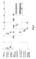
- Fig. 3 is a block diagram illustrating one example of the above-described conventional cache devices.
- an instruction control unit 2 handles instructions one after another in order under the command of a program counter, and when a given instruction to be handled is concerted with the fetch of data from a main memory, it registers the address of a main memory to be accessed into an EA (Effective Address) register 11.
- EA Effective Address
- the address to be registered into EA register 11 is constituted of three kinds of address data: one is an intra-block address which indicates the address within block data to be fetched, a second one is a cache index address which determines the access address of a cache using block data as basic units, and the third is a tag address which uses the cache capacity as a basic unit and employs an address exceeding the cache capacity as a search address.
- the address of an address array 12 is utilized as an index by which a corresponding cash index address of EA register 11 is referred to.
- An address which has been obtained after a search through the address array 12 is compared With a corresponding tag address of EA register by a comparator 13.
- a comparator 13 When it is found as a result of comparison that the two are identical, namely, when a cache hit occurs, it indicates that desired data is in the cache.
- the desired data must be fetched from a main memory.
- the tag data read from the address array 12 is compared with the corresponding tag data of EA register 11, and, when the two are identical, the hit result is delivered to a hit/miss register 14 for registration.
- the cache index address of EA register 11 is registered into EA1 register 16.
- Corresponding data of data array 22 are read with reference to the address of EA1 register, and a selector 23a selects desired data from data read from the data array 22, depending on the hit data provided by the hit/miss register 14, and places it in a register A 24. Then, the selected data is written through a register B5 into a general purpose register 7a.
- the tag data read from the address array 12 is compared with the corresponding tag data of EA register 11, and, when the two are not identical, the miss result is delivered to the hit/miss register 14 for registration.
- a start signal to fetch data from the main memory which is generated as a result of miss occurrence is delivered to an address control unit 3.
- the addresses of data which are to be fetched as block data from the main memory are delivered from EA register 11 to the address control unit 3.
- the address control unit 3 converts the logic addresses into physical addresses, fetches block data from the main memory 4 and places them into a cache device la.
- the selector 15a selects write addresses delivered through a signal line 31, and data received by a reply register 17 are written into the data array 22.
- the selector 15a selects a write address of EA register 11, and the selector 21a selects a corresponding write data of signal line 32, and writes it into the data array 22.
- the main memory 4 is connected to the other information processing units, and, when access requests arrive from different units, competition for processing arises over the main memory. As a result, block load data returned from the main memory to the cache device will arrive in an irregular order.
- Block load data returned to compensate for a request resulting in a cache miss occur as a cluster of eight reply data, and the cluster comprising eight reply data contains desired data (to be referred to as target data hereinafter) to be written into the general purpose register 7.
- target data is returned from the main memory 4, it is received temporarily by the reply register 17, and written via registers A 24 and B 5 into the general purpose register 7a.
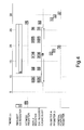
- Fig. 4 is a timing chart representing the operation of cache device la described above.
- a request for data fetch from the main memory is dispatched by the instruction control unit 2 and judged to encounter a cache miss at timing 2, and the cache miss is registered into the hit/miss register 14.
- address conversion is performed by the address control unit 3
- logical addresses are converted into physical addresses, and from corresponding addresses of the main memory 4
- block load data are fetched.
- data a3 returns at timing 9, data a2 at timing 10, data a5 at timing 13, data al at timing 17, data a6 at timing 18, data a4 at timing 22, data a7 at timing 23 and data a8 at timing 26.
- cache busy signals are continuously asserted from timing 9 until the whole block load data have been received by the cache. In this particular example, cache busy signals are relieved when timing 26 is reached.
- a subsequent request for fetch of data from the main memory 4 arise at timing 12. Because the cache busy signal continues to be active from the timing 9 to the timing 26, the subsequent requests are ignored, and no request is executed until timing 27 when cash busy signals are relieved.
- cache search is practiced for one of the subsequent requests for data fetch from the main memory, and when it is found that it meets a cache hit, the target data is read from the data array, and at timing 31 that data is written into the general purpose register 7.
- the conventional cache device whose operation proceeds as described above has the following problems.
- a cache device incorporating a non-blocking mechanism which can manage, even when a cache miss occurs, subsequent memory access instructions without ignoring them, the desired data (the target data) contained in block data returned from the main memory to compensate for the cache miss must be written into the general purpose register 7.
- the cache incorporates a non-blocking mechanism, at least one subsequent data fetch instruction may access to the cache.
- the target data delivered from the main memory 4 and the data selected in response to the subsequent fetch instructions may compete for the path to the general purpose register.
- cache access by any subsequent data fetch instruction is inhibited, and the registration of target data in the block data fetched from the main memory is allowed to take a precedence.
- the target data of the block load data is returned to the cache, access of the cache by subsequent instructions is inhibited, which leads to a lowered efficiency of memory access management.
- the cache is so constructed as to allow an identical path to act at the same time as a data path for data returned from the main memory, and as an access path when a cache hit occurs. Further, when block data returned from the main memory are directly stored in the cache, it may happen that cache busy signals are activated continuously for a long time, and in the mean time execution of subsequent instructions for fetch of data from the main memory is arrested. This is to prevent those subsequent instructions from getting access to the cache because data may arrive at the cache any time from the main memory.
- the object of this invention is to provide, as a remedy for the above problems, a cache device with which it is possible to reduce the time during which access of the cache by data fetch instructions occurring after a cache miss must be inhibited, and thus it is possible to reduce the time necessary for the subsequent instructions to wait for their turn of cache access.
- a cache device connected between a processing unit and a main memory unit, the cache device comprising a holding means which holds block data partially transferred from said main memory unit and including desired data indicated by an instruction when cache access by said instruction results in a cache miss, said instruction is issued by said processing unit and instructs to access said main memory, a delivery means which delivers said desired data to said processing unit when said desired data is transferred from said main memory unit, and a control means which writes said block data into a data array when the whole content of said block data is accumulated in said holding means, and inhibits cache access by one or more new instructions while said block data are written into said data array.
- the cache device of the present invention has a means which will return target data to the general purpose register in a short period through a bypass, if a foregoing request for fetch of data from the main memory encounters a cache miss, and subsequent requests for fetch of data from the main memory occur just at a timing when block data to compensate for the cache miss are returned to the data array, and thus allows writing of the data into the general purpose register to occur not only through a cache hit path but also through a path specially dedicated for block data returned from the main memory.
- the cache device of the present invention ensures the continuation of handling of subsequent requests for fetch of data from the main memory even when a cache miss occurs, and those requests appear at a timing when the fetch of data from the main memory to compensate for the cache miss takes place.
- the cache device of the present invention has a data buffer to hold block data fetched from the main memory, and a bypass or a path through which writing of the block data into the general purpose register is achieved, it is possible for the block data to be written into the general purpose register without competing for access to the register.
- the cache device of the present invention has a cache hit path and a cache miss pass separately so that data can be safely written into the general purpose register, and temporarily stores block load data returned from the main memory in an irregular order into the data buffer so that the data can be written later into the cache without any interruptions.
- a cache device 1 includes a data buffer 18, a first bypass 33, a selector 19, a second bypass 34, a first control means (a target data bypass control circuit 25), and a second control means (a data array write control circuit 26).
- the cache device in response to an access instruction to a main memory issued by an instruction control unit 2, writes target data designated by the main memory access instruction into a general purpose register 7.
- the data buffer 18 holds data sent from the main memory 4.
- the first bypass 33 is a bypass through which data dispatched by the main memory 4 are sent directly to the selector 19 circumventing the data buffer 18.
- the selector 19 receives data sent from the data buffer 18 or data sent by way of the first bypass 33, chooses appropriate ones from them and dispatches them as an output.
- the second bypass 34 guides output dispatched by the selector 19 to the general purpose register 7.
- the first control means, the target data bypass control circuit 25, writes the target data into the general purpose register 7 by way of the first and second bypasses 33 and 34.
- the second control means, data array write control circuit 26, once whole block load data sent from the main memory 4 have been held in the data buffer 18, inhibits the execution of subsequent instructions for access to the main memory, and writes the block load data held in the data buffer 18 into the data array 22.
- the general purpose register 7 is a software visible register, and has input ports for data from the data array 22 and from the bypass 34.
- the instruction control unit 2 processes instructions one after another in order under the command of a program counter. Briefly, description will be given assuming that this example comprises a set of one cache device 1 and one instruction control unit 2. In reality, however, a plurality of sets of the cache device 1 and the instruction control unit 2 are connected to a main memory 4. Futhermore, a plurality of the instruction control unit 2 may be connected to one cache 1 device 1.
- the instruction control unit 2 when instructed to fetch data from the main memory, registers the addresses to be accessed in the main memory into an EA (Effective Address) register 11.
- the address to be registered into EA register 11 contains three kinds of address data: the first one is an intra-block address which indicates an address within block data to be fetched, the second is a cache index address which determines the access address of cache using block data as basic units, and the third is a tag address which uses the cache capacity as a basic unit and employs an address exceeding the cache capacity as a search address.
- the address of address array 12 is used as an index by which a corresponding cache index address of EA register 11 is referred to, and an address obtained after a search through the address array 12 is compared with a corresponding tag address of EA register by a comparator 13.
- the hit result is registered as a hit data into a hit/miss register 14.
- the cache index address of EA register 11 is registered into EA1 register 16.
- Corresponding data of data array 22 are read according to said address registered into EA1 register 16, and the selector 23 selects the desired data from the data read from the data array 22 according to the hit data from the hit/miss register 14, and registers it into a register A 24. Later, the thus selected data is written into the general purpose register 7 by way of a register B 5.
- miss result is registered as a miss data into the hit/miss register 14, which, in response to the miss data, asserts a signal to the address control unit 3 so that fetch of data from the main memory may occur.
- EA register 11 sends to the address control unit 3 the addresses of main memory from which block data are to be fetched.
- the address control unit 3 translates the logical addresses into physical addresses, and delivery of block data from the main memory 4 to the cache device 1 takes place.
- the main memory 4 is constituted of a plurality of banks, and the banks are accessed by interleaving.
- the main memory 4 is connected to other information processing units, and when access requests from different units arrive competition for data fetch arises over the main memory 4.
- block load data transferred from the main memory 4 to the cache device 1 will appear in an irregular order. More specifically, because the aforementioned block load data are controlled in terms of basic data units (e.g., eight bytes), no restrictions are imposed on the order by which the block load data return to the cache. Accordingly, the cache device 1 randomly receives eight reply data (assuming eight for illustration), which constitute the block load data, in response to a cache miss request.
- the block load data constituted by eight reply data contains the desired data (the target data) to be written into the general purpose register 7. While the target data is being returned from the main memory 4, it is received once by a reply register 17, and is sent, under the instruction from a target data bypass control circuit 25, directly to the general purpose register 7 via a bypass 33 and selector 19. Namely, the target data, after having passed through the bypass 33, is written into the general purpose register 7 via a register C 20, bypass 34 and register D 6.
- the cache device 1 stores the block load data in the data buffer 18 until the whole contents of the block load data are accumulated therein, and when storage of all involved data has been achieved, writes them into the data array 22. During this writing process, to prevent subsequent instructions for fetching data from the main memory from getting access to the cache, cache busy signals are asserted.
- the data array write control circuit 26 instructs a selector 21 to guide the data to the data array 22, and instructs another selector 15 so that addresses delivered through a signal line 35 may be registered into EA 1 register 16. Then, the same data array write control circuit 26, using the data of EA 1 register as addresses, writes the data delivered by the selector 21 into the data array 22.
- Cache busy signals to prevent the cache from further being accessed are prepared as eight t sets because the block load data is constituted by eight units, and because each units is transfered per one t.
- a request for data fetch from the main memory is dispatched from the instruction control unit 2 and judged to encounter a cache miss at timing 2, and the cache miss is registered into the hit/miss register 14.
- data a3 returns at timing 9, data a2 at timing 10, data a5 at timing 13, data al at timing 17, data a6 at timing 18, data a4 at timing 22, data a7 at timing 23 and data a8 at timing 26 ( assuming al is the target data for illustration).
- cache busy signals are set into play at timing 27, and the block load data are read sequentially from the data buffer 18. The thus read data are continuously fed to the data array 22 for storage.
- supply of data to the data array is completed, and thus cache busy signals are activated during the interval of 8t spanning from timing 27 to 34, and on cessation of the interval the signals are withdrawn.
- a subsequent request for data fetch from the main memory appears at timing 12.
- cache busy signals are not yet activated, and thus in response to the request in question, a search for data in cache starts at timing 12.
- desired data is read from the data array, and written into the general purpose register 7 at timing 16.
- the cache device of the present invention can reduce the time during which, when a foregoing request encounters a cache miss, access to the cache by subsequent requests must be blocked, and thus it is possible to reduce the time necessary or a given subsequent request to wait before it can gain access to the cache.
- a return path through which pass block load data fetched from the main memory in response to a request for data fetch from the main memory is provided separately from a path through which data are read as a result of a cache hit, and the block load data, after having been temporarily stored in the data buffer, are written sequentially into the data array.
- This arrangement makes it possible to reduce the time during which cache busy signals must be activated. Accordingly, this cache device is advantageous in improving the information handling capacity of the overall information processing system.
Abstract
Description
Claims (9)
- A cache device connected between a processing unit and a main memory unit, said cache device comprising:a holding means which holds block data partially transferred from said main memory unit and including desired data indicated by an instruction when cache access by said instruction results in a cache miss, said instruction being issued by said processing unit and instructing to access said main memory;a delivery means which delivers said desired data to said processing unit when said desired data is transferred from said main memory unit; anda control means which writes said block data into a data array when the whole content of said block data is accumulated in said holding means, and inhibits cache access by one or more new instructions while said block data are written into said data array.
- The cache device as claimed in claim 1 wherein said block data comprise a plurality of data units which are randomly transferred from said main memory unit, and said control means successively writes said plurality of data units held by said holding means into said data array.
- The cache device as claimed in claim 1 wherein said delivery means includes a bypass which circumvents said holding means.
- The cache device as claimed in claim 1 wherein said delivery means includes a first bypass which circumvents said holding means, and a second bypass which circumvents said data array.
- The cache device as claimed in claim 3, further comprising a selector which selects the data outputted from said holding means to write said block data into said data array, and which selects the data delivered through said bypass to deliver said desired data to said processing unit.
- A cache device which continually executes access to a main memory unit by new instructions when a cache miss occurs, said cache device comprising:a buffer which holds block data transferred from said main memory unit; anda control means which writes said block data held by said buffer into a data array when said block data is held in said buffer, and inhibits new accesses to said main memory unit while said block data is written into said data array.
- The cache device as claimed in claim 6 wherein said block data comprise a plurality of data units which are randomly transferred from said main memory unit, and said control means successively writes said plurality of data units held by said buffer into said data array.
- A cache device which writes a desired data into a general purpose register, said desired data being designated by an instruction for accessing a main memory issued by a processing unit, said cache device comprising:a data buffer which holds block data containing said desired data transferred from said main memory when said desired data is found to be absent from a data array;a first bypass which circumvents said data buffer and through which said block data pass;a selector which selects either the data sent by said data buffer or the data sent through said first bypass;a second bypass which guides the data selected by said selector to the general purpose register;a first control means which writes said desired data into said general purpose register through the first and second bypasses; anda second control means which writes said block data held by said data buffer into a data array as soon as said data buffer holds the whole of said block data transferred from said main memory, and which inhibits execution of new instructions for access to said main memory while said block data are written into said data array.
- The cache device as claimed in claim 8 wherein said first control means makes said selector select said data delivered through said first bypass when said desired data is transferred from said main memory unit.
Applications Claiming Priority (3)
| Application Number | Priority Date | Filing Date | Title |
|---|---|---|---|
| JP15857797A JP3481425B2 (en) | 1997-06-16 | 1997-06-16 | Cache device |
| JP158577/97 | 1997-06-16 | ||
| JP15857797 | 1997-06-16 |
Publications (3)
| Publication Number | Publication Date |
|---|---|
| EP0884683A2 true EP0884683A2 (en) | 1998-12-16 |
| EP0884683A3 EP0884683A3 (en) | 1999-07-21 |
| EP0884683B1 EP0884683B1 (en) | 2002-10-16 |
Family
ID=15674737
Family Applications (1)
| Application Number | Title | Priority Date | Filing Date |
|---|---|---|---|
| EP98250210A Expired - Lifetime EP0884683B1 (en) | 1997-06-16 | 1998-06-16 | Cache device |
Country Status (5)
| Country | Link |
|---|---|
| US (1) | US6154814A (en) |
| EP (1) | EP0884683B1 (en) |
| JP (1) | JP3481425B2 (en) |
| CA (1) | CA2240634C (en) |
| DE (1) | DE69808700T2 (en) |
Families Citing this family (6)
| Publication number | Priority date | Publication date | Assignee | Title |
|---|---|---|---|---|
| US6014759A (en) * | 1997-06-13 | 2000-01-11 | Micron Technology, Inc. | Method and apparatus for transferring test data from a memory array |
| US6044429A (en) | 1997-07-10 | 2000-03-28 | Micron Technology, Inc. | Method and apparatus for collision-free data transfers in a memory device with selectable data or address paths |
| US6757817B1 (en) * | 2000-05-19 | 2004-06-29 | Intel Corporation | Apparatus having a cache and a loop buffer |
| US6933945B2 (en) * | 2003-03-31 | 2005-08-23 | Sun Microsystems, Inc. | Design for a non-blocking cache for texture mapping |
| US7174426B2 (en) * | 2003-07-24 | 2007-02-06 | International Business Machines Corporation | Interleave pre-checking in front of shared caches with pipelined access |
| US7167952B2 (en) * | 2003-09-17 | 2007-01-23 | International Business Machines Corporation | Method and system for performing a memory-mode write to cache |
Citations (2)
| Publication number | Priority date | Publication date | Assignee | Title |
|---|---|---|---|---|
| EP0304587A2 (en) * | 1987-08-24 | 1989-03-01 | International Business Machines Corporation | Interruptible cache loading |
| US5454093A (en) * | 1991-02-25 | 1995-09-26 | International Business Machines Corporation | Buffer bypass for quick data access |
Family Cites Families (7)
| Publication number | Priority date | Publication date | Assignee | Title |
|---|---|---|---|---|
| JPS62102344A (en) * | 1985-10-29 | 1987-05-12 | Fujitsu Ltd | Buffer memory control system |
| JPH0415844A (en) * | 1990-05-09 | 1992-01-21 | Nec Ibaraki Ltd | Cache memory control circuit |
| JPH0447350A (en) * | 1990-06-12 | 1992-02-17 | Nec Ibaraki Ltd | Main storage read/response control |
| JPH04293136A (en) * | 1991-03-20 | 1992-10-16 | Nec Ibaraki Ltd | Cache control system |
| JPH0769863A (en) * | 1993-08-27 | 1995-03-14 | Dainippon Jochugiku Co Ltd | Liquid cloudy bathing agent |
| JPH08221328A (en) * | 1995-02-10 | 1996-08-30 | Hitachi Ltd | Cache memory device |
| JPH08272608A (en) * | 1995-03-31 | 1996-10-18 | Hitachi Ltd | Pipeline processor |
-
1997
- 1997-06-16 JP JP15857797A patent/JP3481425B2/en not_active Expired - Fee Related
-
1998
- 1998-06-15 CA CA002240634A patent/CA2240634C/en not_active Expired - Fee Related
- 1998-06-16 EP EP98250210A patent/EP0884683B1/en not_active Expired - Lifetime
- 1998-06-16 US US09/097,593 patent/US6154814A/en not_active Expired - Lifetime
- 1998-06-16 DE DE69808700T patent/DE69808700T2/en not_active Expired - Fee Related
Patent Citations (2)
| Publication number | Priority date | Publication date | Assignee | Title |
|---|---|---|---|---|
| EP0304587A2 (en) * | 1987-08-24 | 1989-03-01 | International Business Machines Corporation | Interruptible cache loading |
| US5454093A (en) * | 1991-02-25 | 1995-09-26 | International Business Machines Corporation | Buffer bypass for quick data access |
Also Published As
| Publication number | Publication date |
|---|---|
| JPH117410A (en) | 1999-01-12 |
| CA2240634A1 (en) | 1998-12-16 |
| JP3481425B2 (en) | 2003-12-22 |
| EP0884683B1 (en) | 2002-10-16 |
| CA2240634C (en) | 2002-08-13 |
| EP0884683A3 (en) | 1999-07-21 |
| DE69808700D1 (en) | 2002-11-21 |
| US6154814A (en) | 2000-11-28 |
| DE69808700T2 (en) | 2003-06-12 |
Similar Documents
| Publication | Publication Date | Title |
|---|---|---|
| US7133981B2 (en) | Prioritized bus request scheduling mechanism for processing devices | |
| US4805098A (en) | Write buffer | |
| CA1286784C (en) | Cache storage queue | |
| US6732242B2 (en) | External bus transaction scheduling system | |
| US5664148A (en) | Cache arrangement including coalescing buffer queue for non-cacheable data | |
| EP0514024A2 (en) | Method and apparatus for an improved memory architecture | |
| US5446844A (en) | Peripheral memory interface controller as a cache for a large data processing system | |
| EP0283891B1 (en) | Cache memory with hit predictive logic | |
| JPH11272555A (en) | Cache memory control system | |
| EP0884683B1 (en) | Cache device | |
| EP0600165B1 (en) | Vector processing device | |
| JPH06318174A (en) | Cache memory system and method for performing cache for subset of data stored in main memory | |
| EP0279189A2 (en) | Storage system | |
| US4802125A (en) | Memory access control apparatus | |
| US4737908A (en) | Buffer memory control system | |
| JPH0756808A (en) | Data cache buffer and storage method | |
| JPS6349945A (en) | Process roll-in system for data processor | |
| US20010039558A1 (en) | Cache memory management method for real time operating system | |
| JP2972451B2 (en) | Cache memory control method by hardware control software | |
| JPH08272667A (en) | File access control system | |
| JPH0833868B2 (en) | Data transfer device | |
| JP2000090007A (en) | Cache control system, its reading method and record medium recording its control program | |
| JPH06149673A (en) | Cache control system | |
| JPH0877072A (en) | Cache memory device | |
| JPH05334185A (en) | Three-hierarchcial memory system |
Legal Events
| Date | Code | Title | Description |
|---|---|---|---|
| PUAI | Public reference made under article 153(3) epc to a published international application that has entered the european phase |
Free format text: ORIGINAL CODE: 0009012 |
|
| AK | Designated contracting states |
Kind code of ref document: A2 Designated state(s): DE FR GB IT NL |
|
| AX | Request for extension of the european patent |
Free format text: AL;LT;LV;MK;RO;SI |
|
| PUAL | Search report despatched |
Free format text: ORIGINAL CODE: 0009013 |
|
| AK | Designated contracting states |
Kind code of ref document: A3 Designated state(s): AT BE CH CY DE DK ES FI FR GB GR IE IT LI LU MC NL PT SE |
|
| AX | Request for extension of the european patent |
Free format text: AL;LT;LV;MK;RO;SI |
|
| 17P | Request for examination filed |
Effective date: 19990727 |
|
| 17Q | First examination report despatched |
Effective date: 19991227 |
|
| AKX | Designation fees paid |
Free format text: DE FR GB IT NL |
|
| GRAG | Despatch of communication of intention to grant |
Free format text: ORIGINAL CODE: EPIDOS AGRA |
|
| GRAG | Despatch of communication of intention to grant |
Free format text: ORIGINAL CODE: EPIDOS AGRA |
|
| GRAH | Despatch of communication of intention to grant a patent |
Free format text: ORIGINAL CODE: EPIDOS IGRA |
|
| GRAH | Despatch of communication of intention to grant a patent |
Free format text: ORIGINAL CODE: EPIDOS IGRA |
|
| GRAA | (expected) grant |
Free format text: ORIGINAL CODE: 0009210 |
|
| AK | Designated contracting states |
Kind code of ref document: B1 Designated state(s): DE FR GB IT NL |
|
| REG | Reference to a national code |
Ref country code: GB Ref legal event code: FG4D |
|
| REF | Corresponds to: |
Ref document number: 69808700 Country of ref document: DE Date of ref document: 20021121 |
|
| ET | Fr: translation filed | ||
| PLBE | No opposition filed within time limit |
Free format text: ORIGINAL CODE: 0009261 |
|
| STAA | Information on the status of an ep patent application or granted ep patent |
Free format text: STATUS: NO OPPOSITION FILED WITHIN TIME LIMIT |
|
| 26N | No opposition filed |
Effective date: 20030717 |
|
| PGFP | Annual fee paid to national office [announced via postgrant information from national office to epo] |
Ref country code: FR Payment date: 20060608 Year of fee payment: 9 Ref country code: DE Payment date: 20060608 Year of fee payment: 9 |
|
| PGFP | Annual fee paid to national office [announced via postgrant information from national office to epo] |
Ref country code: GB Payment date: 20060614 Year of fee payment: 9 |
|
| PGFP | Annual fee paid to national office [announced via postgrant information from national office to epo] |
Ref country code: NL Payment date: 20060615 Year of fee payment: 9 |
|
| PGFP | Annual fee paid to national office [announced via postgrant information from national office to epo] |
Ref country code: IT Payment date: 20060630 Year of fee payment: 9 |
|
| GBPC | Gb: european patent ceased through non-payment of renewal fee |
Effective date: 20070616 |
|
| NLV4 | Nl: lapsed or anulled due to non-payment of the annual fee |
Effective date: 20080101 |
|
| REG | Reference to a national code |
Ref country code: FR Ref legal event code: ST Effective date: 20080229 |
|
| PG25 | Lapsed in a contracting state [announced via postgrant information from national office to epo] |
Ref country code: NL Free format text: LAPSE BECAUSE OF NON-PAYMENT OF DUE FEES Effective date: 20080101 Ref country code: DE Free format text: LAPSE BECAUSE OF NON-PAYMENT OF DUE FEES Effective date: 20080101 |
|
| PG25 | Lapsed in a contracting state [announced via postgrant information from national office to epo] |
Ref country code: GB Free format text: LAPSE BECAUSE OF NON-PAYMENT OF DUE FEES Effective date: 20070616 |
|
| PG25 | Lapsed in a contracting state [announced via postgrant information from national office to epo] |
Ref country code: FR Free format text: LAPSE BECAUSE OF NON-PAYMENT OF DUE FEES Effective date: 20070702 |
|
| PG25 | Lapsed in a contracting state [announced via postgrant information from national office to epo] |
Ref country code: IT Free format text: LAPSE BECAUSE OF NON-PAYMENT OF DUE FEES Effective date: 20070616 |