EP0881670A2 - Hilfsseitenwandabstandsstück für integrierte Schaltungstransistoren - Google Patents
Hilfsseitenwandabstandsstück für integrierte Schaltungstransistoren Download PDFInfo
- Publication number
- EP0881670A2 EP0881670A2 EP98303846A EP98303846A EP0881670A2 EP 0881670 A2 EP0881670 A2 EP 0881670A2 EP 98303846 A EP98303846 A EP 98303846A EP 98303846 A EP98303846 A EP 98303846A EP 0881670 A2 EP0881670 A2 EP 0881670A2
- Authority
- EP
- European Patent Office
- Prior art keywords
- gate electrode
- layer
- forming
- oxide
- conformal
- Prior art date
- Legal status (The legal status is an assumption and is not a legal conclusion. Google has not performed a legal analysis and makes no representation as to the accuracy of the status listed.)
- Withdrawn
Links
Images


Classifications
-
- H—ELECTRICITY
- H10—SEMICONDUCTOR DEVICES; ELECTRIC SOLID-STATE DEVICES NOT OTHERWISE PROVIDED FOR
- H10W—GENERIC PACKAGES, INTERCONNECTIONS, CONNECTORS OR OTHER CONSTRUCTIONAL DETAILS OF DEVICES COVERED BY CLASS H10
- H10W20/00—Interconnections in chips, wafers or substrates
- H10W20/01—Manufacture or treatment
- H10W20/031—Manufacture or treatment of conductive parts of the interconnections
- H10W20/069—Manufacture or treatment of conductive parts of the interconnections by forming self-aligned vias or self-aligned contact plugs
-
- H—ELECTRICITY
- H10—SEMICONDUCTOR DEVICES; ELECTRIC SOLID-STATE DEVICES NOT OTHERWISE PROVIDED FOR
- H10D—INORGANIC ELECTRIC SEMICONDUCTOR DEVICES
- H10D30/00—Field-effect transistors [FET]
- H10D30/01—Manufacture or treatment
- H10D30/021—Manufacture or treatment of FETs having insulated gates [IGFET]
- H10D30/0223—Manufacture or treatment of FETs having insulated gates [IGFET] having source and drain regions or source and drain extensions self-aligned to sides of the gate
- H10D30/0227—Manufacture or treatment of FETs having insulated gates [IGFET] having source and drain regions or source and drain extensions self-aligned to sides of the gate having both lightly-doped source and drain extensions and source and drain regions self-aligned to the sides of the gate, e.g. lightly-doped drain [LDD] MOSFET or double-diffused drain [DDD] MOSFET
-
- H—ELECTRICITY
- H10—SEMICONDUCTOR DEVICES; ELECTRIC SOLID-STATE DEVICES NOT OTHERWISE PROVIDED FOR
- H10D—INORGANIC ELECTRIC SEMICONDUCTOR DEVICES
- H10D84/00—Integrated devices formed in or on semiconductor substrates that comprise only semiconducting layers, e.g. on Si wafers or on GaAs-on-Si wafers
- H10D84/01—Manufacture or treatment
- H10D84/0123—Integrating together multiple components covered by H10D12/00 or H10D30/00, e.g. integrating multiple IGBTs
- H10D84/0126—Integrating together multiple components covered by H10D12/00 or H10D30/00, e.g. integrating multiple IGBTs the components including insulated gates, e.g. IGFETs
- H10D84/0165—Integrating together multiple components covered by H10D12/00 or H10D30/00, e.g. integrating multiple IGBTs the components including insulated gates, e.g. IGFETs the components including complementary IGFETs, e.g. CMOS devices
- H10D84/0184—Manufacturing their gate sidewall spacers
-
- H—ELECTRICITY
- H10—SEMICONDUCTOR DEVICES; ELECTRIC SOLID-STATE DEVICES NOT OTHERWISE PROVIDED FOR
- H10D—INORGANIC ELECTRIC SEMICONDUCTOR DEVICES
- H10D84/00—Integrated devices formed in or on semiconductor substrates that comprise only semiconducting layers, e.g. on Si wafers or on GaAs-on-Si wafers
- H10D84/01—Manufacture or treatment
- H10D84/02—Manufacture or treatment characterised by using material-based technologies
- H10D84/03—Manufacture or treatment characterised by using material-based technologies using Group IV technology, e.g. silicon technology or silicon-carbide [SiC] technology
- H10D84/038—Manufacture or treatment characterised by using material-based technologies using Group IV technology, e.g. silicon technology or silicon-carbide [SiC] technology using silicon technology, e.g. SiGe
-
- H—ELECTRICITY
- H10—SEMICONDUCTOR DEVICES; ELECTRIC SOLID-STATE DEVICES NOT OTHERWISE PROVIDED FOR
- H10W—GENERIC PACKAGES, INTERCONNECTIONS, CONNECTORS OR OTHER CONSTRUCTIONAL DETAILS OF DEVICES COVERED BY CLASS H10
- H10W20/00—Interconnections in chips, wafers or substrates
- H10W20/01—Manufacture or treatment
- H10W20/031—Manufacture or treatment of conductive parts of the interconnections
- H10W20/0698—Local interconnections
Definitions
- the present invention relates generally to the formation of integrated circuit structures, and more specifically to a technique for forming self-aligned contacts and integrated circuit devices.
- the technique is particularly adapted for use with very small device geometries.
- Self-aligned structures have been used in the formation of better contacts. However, at continually shrinking device sizes, even self-aligned contacts have problems.
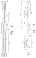
- a substrate 10 contains field oxide regions 12 , 14 which define an active region between them. Within the active region, a transistor is formed by a gate electrode 16 .
- the gate electrode 16 includes a gate oxide layer on the surface of a substrate 10 , with a doped polycrystalline silicon layer 20 above it. This is all that is required to define a gate electrode, but many structures also contain a silicide layer 22 to improve conductivity, and a cap oxide layer 24 to protect the gate electrode.
- Sidewall oxide spacers 26 are formed alongside the electrode 16 , and are used in the formation of LDD regions 28 .
- Highly doped source/drain regions 30 are formed outside the LDD regions as is known in the art.
- Oxide layer 32 is formed over the entire device, and an opening 34 is formed in it to create a contact to one of the source drain regions 30 .
- Oxide layer 32 is a conformal oxide layer deposited as known in the art, and is often referred to as an interpoly oxide (IPO) layer.
- IP interpoly oxide
- a sidewall region 36 remains alongside sidewall spacer 26 .
- Sidewall region 36 has a thickness approximately equal to the deposited thickness of IPO layer 32 .
- Sidewall region 36 causes a smaller surface area to be available for contact to the source drain region 30 . Because the devices are typically made as small as possible, it is not desirable to increase the surface area of the source drain region 30 to simply provide a more area for the contact. However, it is not realistic to try to remove the sidewall region 36 ; over etching or use of a wet etch will tend to damage the substrate as well as surrounding oxide regions. Thus, the space available for contact is made smaller by the area taken up by the sidewall region 36 .
- An improved processing technique results in a structure which maximizes contact area by eliminating a sidewall spacer used to form LDD regions.
- a sacrificial spacer is provided during processing to form the LDD regions, and is then removed prior to further processing of the device.
- a sidewall spacer is then formed in a self-aligned contact from a later deposited oxide layer used as an interlevel dielectric. This leaves only a single oxide sidewall spacer alongside the gate electrode, maximizing the surface area available for the self-aligned contact itself.
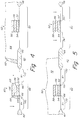
- field oxide regions 42 , 44 , 46 within a substrate 40 are formed field oxide regions 42 , 44 , 46 .
- Active region 48 formed between field oxide regions 42 and 44 , will be used for fabrication of an n-channel field effect device.
- Active region 50 will be used for formation of a p-channel field effect device.
- a thermal gate oxide layer 52 is grown over the device as known in the art. Gate oxide layer 52 may be grown using any known techniques, including formation of an oxide-nitride-oxide layer if desired. Polycrystalline silicon layer 54 is then deposited over the device, and doped to provide a desired conductivity. Doping of polycrystalline silicon layer 54 may be done by implant, or using any other technique known in the art.
- a silicide layer 56 may be formed over the polycrystalline layer 54 as known in the art. Any of the several well known techniques for forming a refractory metal silicide layer 56 may be used. A protective cap oxide layer 58 is then formed over the device, resulting in the structure shown in Figure 2 . Processing to this point is conventional.
- the stack just formed is patterned and etched to define gate electrodes 60 and 62 .
- Photo resist layer 64 is formed over the p-channel region 50 in order to protect it during the next few processing steps.
- a blanket N- implant is then made over the device, forming LDD regions 66 .
- Photo resist layer 64 protects the p-channel regions 50 from this implant.
- the N- implant is the standard LDD implant well known in the art, and can be, for example, an implant of phosphorus at a dose of 1 - 10 x 10 13 / cm 2 and implant energy of 5 - 40 KV.
- FIG. 3 The processing steps shown in Figure 3 are also essentially conventional. As shown in Figure 4 , however, the method of the present invention now begins to diverge from standard processing, techniques.
- a conformal polymer layer, or amorphous carbon layer is formed over the entire device, and anisotropically etched back. This results in the formation of sidewall spacer region 68 along side gate electrode 60 and photoresist layer 64 .
- the sidewall spacer 68 alongside the gate electrode 60 will function as sacrificial sidewall spacers to be removed shortly.
- the polymer which is used for layer 68 can be parylene, or any similar carbon-based polymer which can be deposited conformally in a plasma. As described above, a layer of amorphous carbon or other material which can be ashed may also be used. In the remainder of this description, it will be understood that such layers are included when the term polymer layer is used.
- the preferred properties of a polymer layer include a good blocking ability for the following implant step, and the ability to be easily removed when photoresist layer 64 is removed.
- the polymer- layer is preferably deposited to a depth of approximately 1000 - 2000 angstroms, resulting in sidewall spacers 68 having a width of approximately 1000 - 2000 angstroms. This defines the width of the LDD regions following the next implant step.
- the polymer should be deposited at a low temperature, preferably less than approximately 130° C, to prevent damage to the resist layer 64 .
- an N+ implant of arsenic or other suitable dopant is made over the device, forming heavily doped source/drain regions 70 .
- the arsenic is implanted at a dose of approximately 3 x 10 15 / cm 2 , and an energy of approximately 40 KV.
- Source/drain regions 70 are spaced from the side of the gate electrode 60 of approximately the thickness of sidewall spacer 68 , as known in the art. At this time, formation of the n-channel device in active region 48 has been completed.
- photoresist layer 64 In order to form the p-channel device, it is necessary to remove photoresist layer 64 . This is typically done by ashing, followed by a short clean up using a chemical such as piranha. These standard cleanup steps will remove all traces of the polymer sidewall regions 68 , so that no sidewall regions remain alongside the gate electrode 60 .
- photoresist layer 72 is deposited over the wafer and patterned, as known in the art, to cover active region 48 and expose active region 50 . If p-type LDD regions are desired, in a manner similar to that described in connection with Figure 3 , a blanket implant of boron is made to form lightly doped drain region 74 for the p-channel device. Typical implants are made at a dose of 1 - 10 x 10 13 / cm 2 , and implant energy of 5 - 30 KV. A conformal polymer layer is then formed over the device in the same manner as described previously, preferably to a thickness of approximately 1000 angstroms, and anisotropically etched back to form sidewall regions 76 .
- Source drain region 78 are then used as spacers for the high dosage boron to implant form P+ source/drain regions 78 .
- a typical dosage for the boron implant is 3 x 10 15 / cm 2 at an energy-of 5 - 30 KV.
- the device now includes gate electrodes 60 and 62 , neither of which have sidewall spacers of any type.
- the desired LDD structures have been formed through the use of sacrificial polymer spacers as described above.
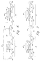
- a conformal dielectric layer 80 is deposited over the entire device. This layer 80 is used as the interpoly oxide (IPO) layer.
- IPO layer 80 is preferably undoped oxide deposited to a thickness of approximately 1000 - 2000 angstroms.
- the IPO layer 80 is patterned and etched with a photoresist layer (not shown) to form contact openings 82 and 84 . Tolerances for formation of these openings is not critical; both of them are self-aligned with respect to the gate electrodes 60 and 62 . That portion of the IPO layer 80 which lies within openings 82 , 84 , alongside the edges of electrodes 60 , 62 , remains behind as sidewall regions 86 , 88 .
- the sidewall spacers 86 , 88 perform isolation functions for the respective gate electrodes 60 , 62 .
- either, both, or neither source/drain region may have a self-aligned contact formed at this time. However, even if a source/drain contact is formed at a later stage, the sidewall spacers 86 , 88 will be formed by the IPO layer 80 if such contact is adjacent the gate electrode.
- a polycrystalline silicon layer is deposited, patterned, and etched as known in the art to form conductive poly electrodes 90 , 92 .
- sidewall spacers 86 , 88 isolate gate electrodes 60 , 62 , respectively, from interconnect leads 90 , 92 .
- the contacts to the underlying substrate 40 are separated from electrodes 60 , 62 only by the thickness of spacers 86 , 88 .
- the use of a sacrificial layer for the LDD sidewall spacers allows the contact to be brought closer to gate electrodes 60 , 62 .
- the structure resulting from the method described above is essentially the same transistor structure as widely available on devices made according to known CMOS processing techniques.
- the sidewall spacers alongside the gate electrodes are narrower, due to the removal of the spacers used to form the LDD regions. This gives a larger contact region, thus reducing contact resistance, or closer spacing of elements which can be used to shrink the overall size of the device.
- the method described herein uses less masking steps than is typical for CMOS process. Usually, all sidewall spacers are formed after both P- and N- LDD implants, requiring masking for both the LDD and source/drain implants.
- the method of the present invention disposes of the sidewalls used to form LDD regions, so only a single mask is needed for both the LDD and source/drain implants. This saves two masking steps over typical prior art techniques.
Landscapes
- Insulated Gate Type Field-Effect Transistor (AREA)
- Metal-Oxide And Bipolar Metal-Oxide Semiconductor Integrated Circuits (AREA)
- Electrodes Of Semiconductors (AREA)
Applications Claiming Priority (2)
| Application Number | Priority Date | Filing Date | Title |
|---|---|---|---|
| US866895 | 1997-05-30 | ||
| US08/866,895 US6022782A (en) | 1997-05-30 | 1997-05-30 | Method for forming integrated circuit transistors using sacrificial spacer |
Publications (2)
| Publication Number | Publication Date |
|---|---|
| EP0881670A2 true EP0881670A2 (de) | 1998-12-02 |
| EP0881670A3 EP0881670A3 (de) | 1998-12-16 |
Family
ID=25348668
Family Applications (1)
| Application Number | Title | Priority Date | Filing Date |
|---|---|---|---|
| EP98303846A Withdrawn EP0881670A3 (de) | 1997-05-30 | 1998-05-15 | Hilfsseitenwandabstandsstück für integrierte Schaltungstransistoren |
Country Status (3)
| Country | Link |
|---|---|
| US (2) | US6022782A (de) |
| EP (1) | EP0881670A3 (de) |
| JP (1) | JPH1145944A (de) |
Cited By (2)
| Publication number | Priority date | Publication date | Assignee | Title |
|---|---|---|---|---|
| EP0945897A1 (de) * | 1998-03-25 | 1999-09-29 | Texas Instruments Incorporated | Organische Gate-Seitenwand-Abstandsstücke |
| WO2002017389A3 (en) * | 2000-08-24 | 2002-05-02 | Infineon Technologies Corp | Disposable spacer technology for device tailoring |
Families Citing this family (13)
| Publication number | Priority date | Publication date | Assignee | Title |
|---|---|---|---|---|
| US6632718B1 (en) * | 1998-07-15 | 2003-10-14 | Texas Instruments Incorporated | Disposable spacer technology for reduced cost CMOS processing |
| US7169711B1 (en) * | 2002-06-13 | 2007-01-30 | Advanced Micro Devices, Inc. | Method of using carbon spacers for critical dimension (CD) reduction |
| US6818519B2 (en) * | 2002-09-23 | 2004-11-16 | Infineon Technologies Ag | Method of forming organic spacers and using organic spacers to form semiconductor device features |
| KR100500448B1 (ko) | 2003-02-06 | 2005-07-14 | 삼성전자주식회사 | 선택적 디스포저블 스페이서 기술을 사용하는 반도체집적회로의 제조방법 및 그에 의해 제조된 반도체 집적회로 |
| US7442577B1 (en) | 2006-02-14 | 2008-10-28 | United States Of America As Represented By The Director, National Security Agency The United | Method of fabricating a patterned device using sacrificial spacer layer |
| KR100744071B1 (ko) * | 2006-03-31 | 2007-07-30 | 주식회사 하이닉스반도체 | 벌브형 리세스 게이트를 갖는 반도체 소자의 제조방법 |
| US7678593B1 (en) * | 2006-09-06 | 2010-03-16 | The United States of America, as represented by the Director, National Security Agency | Method of fabricating optical device using multiple sacrificial spacer layers |
| KR101080903B1 (ko) * | 2006-09-29 | 2011-11-09 | 주식회사 하이닉스반도체 | 플래시 메모리 소자의 고전압 트랜지스터 |
| US20080096337A1 (en) * | 2006-10-06 | 2008-04-24 | Texas Instruments Incorporated | Disposable semiconductor device spacer with high selectivity to oxide |
| JP5446558B2 (ja) * | 2009-08-04 | 2014-03-19 | 富士通セミコンダクター株式会社 | 半導体装置の製造方法 |
| KR101669470B1 (ko) * | 2009-10-14 | 2016-10-26 | 삼성전자주식회사 | 금속 실리사이드층을 포함하는 반도체 소자 |
| US20130175619A1 (en) | 2012-01-06 | 2013-07-11 | International Business Machines Corporation | Silicon-on-insulator transistor with self-aligned borderless source/drain contacts |
| US8877642B2 (en) * | 2013-02-01 | 2014-11-04 | Globalfoundries Inc. | Double-pattern gate formation processing with critical dimension control |
Family Cites Families (10)
| Publication number | Priority date | Publication date | Assignee | Title |
|---|---|---|---|---|
| US4838991A (en) * | 1987-10-30 | 1989-06-13 | International Business Machines Corporation | Process for defining organic sidewall structures |
| JPH02199847A (ja) * | 1989-01-27 | 1990-08-08 | Shin Etsu Polymer Co Ltd | Icチップの実装方法 |
| JPH02199841A (ja) * | 1989-01-28 | 1990-08-08 | Sony Corp | Misトランジスタの製造方法 |
| US4994404A (en) * | 1989-08-28 | 1991-02-19 | Motorola, Inc. | Method for forming a lightly-doped drain (LDD) structure in a semiconductor device |
| US5118382A (en) * | 1990-08-10 | 1992-06-02 | Ibm Corporation | Elimination of etch stop undercut |
| US5055898A (en) * | 1991-04-30 | 1991-10-08 | International Business Machines Corporation | DRAM memory cell having a horizontal SOI transfer device disposed over a buried storage node and fabrication methods therefor |
| EP0782195B1 (de) * | 1991-07-25 | 1999-10-13 | Fujitsu Limited | Herstellungsverfahren für Kondensator mit gestapelter Flossenstruktur und mit reduzierter Flossendicke |
| US5332469A (en) * | 1992-11-12 | 1994-07-26 | Ford Motor Company | Capacitive surface micromachined differential pressure sensor |
| JP3196980B2 (ja) * | 1993-01-12 | 2001-08-06 | 株式会社東芝 | 半導体装置の製造方法 |
| KR960012259B1 (ko) * | 1993-03-13 | 1996-09-18 | 삼성전자 주식회사 | 반도체 장치의 제조방법 |
-
1997
- 1997-05-30 US US08/866,895 patent/US6022782A/en not_active Expired - Lifetime
-
1998
- 1998-05-15 EP EP98303846A patent/EP0881670A3/de not_active Withdrawn
- 1998-05-29 JP JP10150087A patent/JPH1145944A/ja active Pending
-
1999
- 1999-10-05 US US09/412,682 patent/US20010035558A1/en not_active Abandoned
Cited By (2)
| Publication number | Priority date | Publication date | Assignee | Title |
|---|---|---|---|---|
| EP0945897A1 (de) * | 1998-03-25 | 1999-09-29 | Texas Instruments Incorporated | Organische Gate-Seitenwand-Abstandsstücke |
| WO2002017389A3 (en) * | 2000-08-24 | 2002-05-02 | Infineon Technologies Corp | Disposable spacer technology for device tailoring |
Also Published As
| Publication number | Publication date |
|---|---|
| US6022782A (en) | 2000-02-08 |
| US20010035558A1 (en) | 2001-11-01 |
| JPH1145944A (ja) | 1999-02-16 |
| EP0881670A3 (de) | 1998-12-16 |
Similar Documents
| Publication | Publication Date | Title |
|---|---|---|
| EP0681320B1 (de) | Verfahren zur Herstellung eines Widerstands | |
| US6037222A (en) | Method for fabricating a dual-gate dielectric module for memory embedded logic using salicide technology and polycide technology | |
| US5538913A (en) | Process for fabricating MOS transistors having full-overlap lightly-doped drain structure | |
| US5668024A (en) | CMOS device structure with reduced risk of salicide bridging and reduced resistance via use of a ultra shallow, junction extension, ion implantation process | |
| US6337262B1 (en) | Self aligned T-top gate process integration | |
| US4319395A (en) | Method of making self-aligned device | |
| US6136636A (en) | Method of manufacturing deep sub-micron CMOS transistors | |
| US5744395A (en) | Low resistance, self-aligned, titanium silicide structures, using a single rapid thermal anneal procedure | |
| US5406111A (en) | Protection device for an intergrated circuit and method of formation | |
| US5464782A (en) | Method to ensure isolation between source-drain and gate electrode using self aligned silicidation | |
| US5554544A (en) | Field edge manufacture of a T-gate LDD pocket device | |
| US6187619B1 (en) | Method to fabricate short-channel MOSFETs with an improvement in ESD resistance | |
| KR19990066850A (ko) | 서브 미크론 금속 게이트 mos 트랜지스터 및 그의 형성 방법 | |
| US6022782A (en) | Method for forming integrated circuit transistors using sacrificial spacer | |
| EP0400821B1 (de) | Lokalverbindungen für integrierte Schaltungen | |
| EP0356202B1 (de) | MOSFET und dessen Herstellungsverfahren | |
| US5866448A (en) | Procedure for forming a lightly-doped-drain structure using polymer layer | |
| EP0465045B1 (de) | Verfahren zum Herstellen von Feldeffekt-Transistoren für integrierte Schaltungen | |
| US5529941A (en) | Method for making an integrated circuit structure | |
| US6610565B2 (en) | Method of forming a CMOS type semiconductor device | |
| US5668051A (en) | Method of forming poly plug to reduce buried contact series resistance | |
| US6207482B1 (en) | Integration method for deep sub-micron dual gate transistor design | |
| US5705437A (en) | Trench free process for SRAM | |
| US6162694A (en) | Method of forming a metal gate electrode using replaced polysilicon structure | |
| US20050026342A1 (en) | Semiconductor device having improved short channel effects, and method of forming thereof |
Legal Events
| Date | Code | Title | Description |
|---|---|---|---|
| PUAI | Public reference made under article 153(3) epc to a published international application that has entered the european phase |
Free format text: ORIGINAL CODE: 0009012 |
|
| PUAL | Search report despatched |
Free format text: ORIGINAL CODE: 0009013 |
|
| AK | Designated contracting states |
Kind code of ref document: A2 Designated state(s): DE FR GB IT |
|
| AX | Request for extension of the european patent |
Free format text: AL;LT;LV;MK;RO;SI |
|
| AK | Designated contracting states |
Kind code of ref document: A3 Designated state(s): AT BE CH CY DE DK ES FI FR GB GR IE IT LI LU MC NL PT SE |
|
| AX | Request for extension of the european patent |
Free format text: AL;LT;LV;MK;RO;SI |
|
| RAP3 | Party data changed (applicant data changed or rights of an application transferred) |
Owner name: STMICROELECTRONICS, INC. |
|
| RAP1 | Party data changed (applicant data changed or rights of an application transferred) |
Owner name: STMICROELECTRONICS, INC. |
|
| 17P | Request for examination filed |
Effective date: 19990531 |
|
| AKX | Designation fees paid |
Free format text: DE FR GB IT |
|
| 17Q | First examination report despatched |
Effective date: 20040928 |
|
| STAA | Information on the status of an ep patent application or granted ep patent |
Free format text: STATUS: THE APPLICATION HAS BEEN WITHDRAWN |
|
| 18W | Application withdrawn |
Effective date: 20070504 |