EP0875933B1 - Thermal interface pad assembly - Google Patents
Thermal interface pad assembly Download PDFInfo
- Publication number
- EP0875933B1 EP0875933B1 EP98303329A EP98303329A EP0875933B1 EP 0875933 B1 EP0875933 B1 EP 0875933B1 EP 98303329 A EP98303329 A EP 98303329A EP 98303329 A EP98303329 A EP 98303329A EP 0875933 B1 EP0875933 B1 EP 0875933B1
- Authority
- EP
- European Patent Office
- Prior art keywords
- thermal
- resilient material
- assembly
- electronic component
- pad
- Prior art date
- Legal status (The legal status is an assumption and is not a legal conclusion. Google has not performed a legal analysis and makes no representation as to the accuracy of the status listed.)
- Expired - Lifetime
Links
Images





Classifications
-
- H—ELECTRICITY
- H10—SEMICONDUCTOR DEVICES; ELECTRIC SOLID-STATE DEVICES NOT OTHERWISE PROVIDED FOR
- H10W—GENERIC PACKAGES, INTERCONNECTIONS, CONNECTORS OR OTHER CONSTRUCTIONAL DETAILS OF DEVICES COVERED BY CLASS H10
- H10W40/00—Arrangements for thermal protection or thermal control
- H10W40/70—Fillings or auxiliary members in containers or in encapsulations for thermal protection or control
- H10W40/77—Auxiliary members characterised by their shape
Definitions
- the present invention relates to a thermal interface that helps to transfer heat from a heat producing component, such as an integrated circuit (IC), to a heat dissipating component, such as a heat sink or adjacent structure. More specifically, the present invention relates to a composite thermal interface comprised of a template, formed from material such as gap pad material or thermal tape, having cavities filled with a pliable material, such as thermal grease or thermal putty.
- a heat producing component such as an integrated circuit (IC)
- a heat dissipating component such as a heat sink or adjacent structure.
- a composite thermal interface comprised of a template, formed from material such as gap pad material or thermal tape, having cavities filled with a pliable material, such as thermal grease or thermal putty.
- a common method used to maintain electronic components at acceptable operating temperatures is to position a planar surface of the electronic component in contact with a planar surface of a heat removal device, such as a heat sink.
- a heat removal device such as a heat sink.
- this alone does not provide an adequate thermal interface because when two such surfaces are brought together, less than one percent of the surfaces make physical contact. As much as 99% of the surfaces are separated by a layer of interstitial air. Some heat is transferred at the points of contact, but much of the heat has to travel through the interstitial air gaps.
- the total thermal resistance through a thermal interface is the thermal resistance at the thermal interface surface of the electronic component, the thermal resistance at the thermal interface of the heat removal device, and the thermal resistance of the material in the interstitial gaps.
- Air is a poor thermal conductor and has a thermal conductivity of 0.027 W/m°C. It is known in the art, for example from US Patent 4 000 509, to use an interface material to fill the interstitial gaps.
- One of the best classes of interface materials are thermal greases. Thermal greases are made be dispersing thermally conductive ceramic fillers in silicone or hydrocarbon oils to form a paste, and have a thermal conductivity of approximately 3 W/m°C. Ideally, thermal grease is applied to one or both surfaces, and the surfaces are held together by a moderate amount of pressure. For example, it is common to use a spring clip to hold a heat sink to an integrated circuit, with thermal grease between the integrated circuit and the heat sink. Thermal greases are pliable, non-resilient, and do not retain or return to their original shape after being deformed.
- Thermal putty such as the T-putty 500 series of thermally conductive putties manufactured by Thermagon, Incorporated, is somewhat similar to thermal grease, but has several advantages.
- T-putty 502 has a relatively high thermal conductivity of 4 W/m°C and is a soft, pliahle, and non-resilient paste-type material that is designed to transfer heat between parts of a delicate nature where only minimal pressure can be applied.
- Thermal putty is available in sheets of various thicknesses, and is much less messy to work with than thermal grease. Like thermal grease, thermal putty does not retain or return to its original shape after being deformed.
- materials that are electrically conductive are also thermally conductive.
- metals are typically more thermally conductive than plastics.
- electrically conductive materials could also be formed into excellent thermal interface materials.
- thermal interface materials could cause problems if the material were to reach a PCB and short out two or more electrical conductors, especially if the material is messy to work with, such as thermal grease.
- thermal interface materials have relatively high electrical resistances, even though such high resistances necessitate lower thermal conductivities.
- Gap pads are formed from resilient highly-conformable thermally conductive materials. Gap pads return to their original shape after a deflecting force has been removed.
- An example is Gap Pad V0, which is manufactured by the Bergquist Company. While gap pads are much more thermally conductive than air, they are not as thermally conductive as thermal greases or putties. For example, Gap Pad V0 has a thermal conductivity of 0.80 W/m°C at 68948 Pa (10 psi).
- gap pads Another disadvantage of gap pads is that pressure is required to achieve acceptable thermal conduction values. Pressure is required both to force the gap pad material into the interstitial gaps, and compress the gap pad itself to minimize the distance between the electronic component and heat removal device. Pressure is much less critical when using thermal greases or putties as an interface material, because these materials naturally flow into the interstitial gaps, and their non-resilient pliable qualities prevents them from pulling out of the gaps after pressure is removed.
- Thermal tapes are similar to, but typically much thinner than gap pads and are generally used for transferring heat between a single IC and a single heat sink. They are also non-compressible. Therefore, like gap pads, thermal tapes have a defined shape.
- Gap pads and thermal tapes are available with one or both surfaces coated with an adhesive substance or a tacky substance.
- a tacky substance is ideal when it is desirable to hold a gap pad in position while assembling electronic components, while an adhesive substance is used when the gap pad itself is used to mount a heat sink to an electronic component.
- Figure 1 shows prior art circuit assembly 10.
- Assembly 10 includes a PCB 12, IC 14, heat sink 16, and gap pad 18.
- Gap pad 18 provides a thermal interface between integrated circuit 14 and heat sink 16.
- a typical thickness for a gap pad between a single heat sink and a single integrated circuit is 635 ⁇ m (0.025 inches).
- gap pad 18 is not drawn to scale in Figure 1.
- Figure 2 is a prior art circuit assembly 20 that incorporates a thermal can.
- Assembly 20 includes PCB 22, ICs 24 and 26, and thermal can 28.
- Thermal can 28 includes bosses 34 and 36.
- Gap pad 30 provides a thermal interface between boss 34 and IC 24.
- gap pad 32 provides a thermal interface between boss 36 and IC 26.
- a second thermal can may be provided along the bottom side of PCB 22.
- a PCB may have components on both sides, in which case the components and thermal can adjacent the bottom of the PCB would be similar to the components and thermal can adjacent the top of the PCB.
- gap pads 30 and 32 are not drawn to scale in Figure 2.
- thermal can An important factor to consider when using a thermal can is the stack-up tolerances of each element in a stack. For example, there are two stacks in Figure 2, the stack formed by PCB 22, IC 24, gap pad 30, and boss 34 and the stack formed by PCB 22, IC 26, gap pad 32, and boss 36.
- the tolerances that must be considered when calculating the total stack-up tolerance are the tolerances associated with the PCB thickness, the height of the electronic component (including variations in height introduced by assembly), the interface pad thickness, thickness of the thermal can and boss, the PCB warpage, and the planarity of the boss surface, the electronic component surface, and surfaces of the gap pad.
- a significant variation can result from the substitution of one manufacturer's component with a component from another manufacturer, where the two components are not the same height.
- the first method is to use a pliable and non-resilient thermal compound such as thermal grease or thermal putty. These compounds have good thermal conductivity and will conform easily to various tolerance stack-ups. However, since these compounds are non-resilient, and once deformed they will not return to their original shape. This is a critical factor because the thermal expansion and contraction associated with the heating and cooling cycles that occur whenever a device is powered on and then powered off will eventually cause the thermal compound to lose contact with either the electronic component or the boss, thereby degrading the thermal interface.
- An additional problem related to pliable and non-resilient thermal compounds is the difficulty in controlling their shape when performing initial assembly or rework.
- Resilient, conformable materials such as gap pads, solve some of these problems. Since such materials are resilient, they adapt well to heating and cooling cycles because they attempt to return to their original uncompressed shape. In addition they are easy to work and shape during initial assembly or rework.
- the major problem associated with resilient, conformable materials, such as gap pads is that a certain amount of pressure is required at each electronic component to overcome stack-up tolerances and fill interstitial gaps, and the required pressure may generate excessive forces on the electronic components and PCB. Of course, this problem becomes worse as the number of electronic components cooled by a single thermal can increases. The excessive forces are sometimes reduced by machining relieves into the bosses of the thermal can. However, this reduces thermal performance and adds extra manufacturing costs.
- the present invention is a composite thermal interface pad comprised of a template formed from a material that does not lose its shape, such as thermal gap pad material or thermal tape, in which cavities have been formed and filled with a pliable non-resilient material that does lose its shape when deformed, such as thermal grease or thermal putty.
- the spacing and size of the cavities may be tailored to achieve desired elastic properties, stress distributions, and surface interfaces.
- the cavities may be positioned to optimize the thermal characteristics of the thermal interface with respect to the heat distribution pattern of the electronic component that is being cooled.
- a single composite interface pad may be provided with a variety of cavities filled with pliable non-resilient material to cool an array of components, such as an SDRAM array.
- a single composite interface pad having a single cavity filled with pliable non-resilient material may be provided for a single component, such as a CPU thermally coupled to a heat sink.
- the present invention may also be used to provide EMI shielding along the gap formed between the electronic component and the cooling structure.
- the present invention provides EMI shielding within the thermal interface.
- an adjacent structure is provided with projection features that dig into the pliable non-resilient material.
- the projection features ensure a good thermal interface, increase the surface area available for thermal transfer, and minimize the distance between the electronic component and the adjacent structure used for cooling.
- the present invention provides the benefits enjoyed by prior art materials having defined shapes, such as gap pads and thermal tapes, while providing thermal transfer characteristics similar to those found in prior art pliable non-resilient materials such as thermal grease and thermal putty.
- Figure 1 shows a prior art circuit assembly having a thermal interface between an electronic component and a heat sink.
- Figure 2 is a prior art circuit assembly that has a plurality of thermal interfaces between a thermal can and corresponding plurality of electronic components.
- Figure 3 shows the composite thermal pad of the present invention.
- Figure 4A is a sectional view taken along line 4-4 of Figure 3.
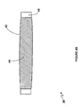
- Figure 4B shows the thermal interface pad of Figure 3 with a cavity therein slightly “overfilled” with pliable non-resilient material.
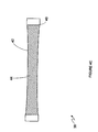
- Figure 4C shows the thermal interface pad of Figure 3 with a cavity therein slightly “underfilled” with non-resilient material.
- Figure 5 shows a heat distribution map of a multi-chip module having two integrated circuits therein.
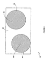
- Figure 6 shows a composite thermal interface pad in accordance with the present invention that has been tailored to match the thermal characteristics of the multi-chip module associated with the thermal distribution map of Figure 5.
- Figure 7 shows a circuit assembly that illustrates another embodiment of the present invention wherein a single composite thermal interface pad provides a thermal interface for a series of electronic components.
- Figure 8 is a top view of the assembly of Figure 7.
- Figure 9 shows a circuit assembly that illustrates an embodiment of the invention in which the gap between an adjacent structure and a printed circuit board is shielded.
- Figure 10 shows a top view of a composite thermal interface pad and a printed circuit from the circuit assembly of Figure 9.
- Figure 11 shows a composite thermal interface pad in accordance with the present invention that includes resilient material and a series of non-resilient material portions, and is adapted for general use in a variety of applications.
- Figure 12 includes a sectional view of the pad of Figure 11 taken along line 12-12 of Figure 11, as well as an electronic component and an adjacent structure having projection features.
- FIG. 3 shows composite thermal pad 38 of the present invention.
- Composite thermal interface pad 38 is comprised of a template portion 40 that includes a cavity 42 that is filled with a pliable non-resilient portion 44.
- the template portion of thermal interface pad 38 is formed from a resilient conformable material, such as gap pad material, and the pliable non-resilient portion is formed from thermal grease or thermal putty.
- the template portion of thermal interface pad 38 is formed from a relatively non-resilient material having a definable shape, such as thermal tape, and the pliable non-resilient portion is formed from thermal grease or thermal putty.
- FIG 4A is a sectional view taken along line 4-4 of Figure 3.
- pliable non-resilient material 44 has the shape of a squat cylinder. Pressure is applied to pliable non-resilient material 44 from beneath by an electronic component, from above by a boss of a thermal can (or other structure), and from the sides by template portion 40.
- template portion 40 is formed from a resilient material, such as gap pad material, portion 40 imparts a certain amount of resiliency to pliable non-resilient material 44. Accordingly, when thermal expansion causes a thermal can boss and top surface of a component to move closer together, the height of the cylinder of non-resilient material 44 decreases, while the diameter of the cylinder increases.
- the present invention combines the two prior art interface materials to form a composite interface pad that has the major advantages of each material, without suffering from the disadvantages associated with either material.
- a block of material may be bored out to form the template pattern, and filled with pliable non-resilient material, after which the block may be sliced into interface pads of any desired thickness.
- cavities may be punched into the material to form the template, and pliable non-resilient material may be applied to the cavities.
- any other methods known in the art may be used.
- pliable non-resilient portion 44 is circular in Figure 3, a variety of other configurations may be used. For example, it may be desirable to provide a cavity having a central hub with a series of spokes emanating from the hub. Such a cavity will better retain the pliable non-resilient material within the template before assembly, as well as provide additional channels (and therefore surface area) within the template cavity for imparting resiliency to the pliable non-resilient material after assembly. Of course, a variety of other shapes may be used, and the invention is not limited to any particular shape.
- the present invention may also be packaged in a manner similar to the manner in which gap pads and thermal tapes are packaged.
- one or both sides of the template portion may be coated with an adhesive or tacky substance.
- liners may be applied to one or both sides of the composite thermal interface pad to protect the adhesive or tacky layers, and to contain the pliable non-resilient material within the template portion.
- FIG. 4B shows thermal interface pad 38 with cavity 42 slightly overfilled with pliable non-resilient material 44. This embodiment is useful when minimal pressure is to be applied to pad 38 because it ensures contact between the electronic component to be cooled and the structure that is conducting away heat, such as a boss on a thermal can.
- Figure 4C shows thermal interface pad 38 with cavity 42 slightly underfilled with pliable non-resilient material 44.
- the embodiment is useful when resilient material (such as gap pad material) will be used to form template portion 40, and will be somewhat more compressed when used in a final assembly. Since pliable non-resilient material 44 will typically be much less compressible than template portion 40 in this embodiment, underfilling cavity 42 helps maintain uniform thickness of the pad after assembly into a product.
- the cavity is filled as shown in Figure 4A, 4B, or 4C (or in some other manner) is a parameter that may be determined by an implementor of the present invention when the present invention is adapted for a particular environment.
- FIG. 5 shows a heat distribution map 46 of a multi-chip module having two integrated circuits in a single module.
- Multi-chip modules in are common in the field of computing.
- Intel's Pentium Pro® CPU is a multi-chip module containing two integrated circuits in a single package.
- Such heat distribution maps are easily generated by viewing an electronic component with an infra-red camera.
- FIG 6 shows a composite thermal interface pad 48 of the present invention that has been tailored to match the thermal characteristics of the multi-chip module associated with thermal distribution map 46 of Figure 5.
- Interface pad 48 is formed from template portion 50 and pliable non-resilient portions 56 and 58. Pliable non-resilient portions 56 and 58 are positioned within cavities 52 and 54 of template portion 50. Note that pliable non-resilient portions 56 and 58 are positioned over the hottest portions of the multi-chip module, as shown in thermal map 46 of Figure 5.
- Figure 7 shows a circuit assembly 60 that illustrates another embodiment of the present invention.
- Assembly 60 includes PCB 62, thermally conductive adjacent structure 64, electronic components 66, 68, 70, and 72, and composite thermal interface pad 74.
- Composite thermal interface pad 74 includes a single template portion 76, and pliable non-resilient portions 78, 80, 82 and 84, which are positioned above electronic components 66, 68, 70, and 72, respectively.
- Figure 8 is a top view of assembly 60 of Figure 7.
- thermally conductive adjacent structure 64 is above composite thermal pad 74, which in turn is above electronic components 66, 68, 70, and 72.
- Composite thermal interface pad 74 has a single template portion 76, and pliable non-resilient portions 78, 80, 82, and 84, with each pliable non-resilient portion centered above an electronic component.
- the embodiment of the present invention shown in Figures 7 and 8 is ideally suited for high density groupings of electronic components, such as an array of SDRAM devices.
- the present invention also provides a unique opportunity to enhance electromagnetic interference shielding (EMI) in the gap area between a PCB and an adjacent structure, such as a thermal can or heat sink.
- EMI electromagnetic interference shielding
- FIG 7 note gap 75 between PCB 62 and adjacent structure 64. EMI from components 66, 68, 70, and 72 may escape via gap 75, even though EMI is otherwise contained by structure 64 and a ground layer of PCB 62 (or some other structure not shown in Figure 7).
- Figure 9 shows a circuit assembly 86 that illustrates an embodiment of the invention in which the gap between an adjacent structure and a PCB is shielded.
- Assembly 86 includes PCB 88, thermally conductive adjacent structure 90, electronic components 92, 94, 96, and 98, and composite thermal interface pad 100.
- Composite thermal interface pad 100 includes a single template portion 102, and pliable non-resilient material portions 104, 106, 108 and 110, which are positioned above electronic components 92, 94, 96, and 98, respectively.
- pad 100 includes a series of pliable non-resilient electrically conductive portions, such as portions 112 and 114.
- template portion 102 is extended to bridge the gap between adjacent structure 90 and PCB board 88.
- pliable non-resilient electrically conductive material portions 112 and 114 are in electrical contact with adjacent structure 90 and a conductive layer of PCB 88.
- Figure 10 shows composite thermal interface pad 100 above PCB 88.
- pad 100 includes a single template portion 102, and pliable non-resilient portions 104, 106, 108 and 110.
- Pliable non-resilient electrically conductive material portions 112 and 114 which are visible in Figure 9, are members of a series of pliable non-resilient electrically conductive portions positioned proximate the outer edge of pad 100. The pliable non-resilient electrically conductive portions also provide good thermal conductivity.
- PCB 88 includes a ground strip that is bounded by dotted line 116 and solid line 118.
- the ground strip may be provided by a foil conductor on PCB 88 and is in electrical contact with each of the pliable non-resilient electrically conductive material portions.
- the pliable non-resilient electrically conductive material portions are also in electrical contact with adjacent structure 90, which is shown in Figure 9.
- the pliable non-resilient electrically conductive material portions of composite thermal interface pad 100 are no more than 0.1 inches apart.
- the gap spacing may be adapted based on the environment in which the present invention will be used.
- FIG 11 shows composite thermal interface pad 120, which illustrates another embodiment of the present invention.
- Pad 120 includes a template portion 122 and a series of pliable non-resilient material portions, such as 124 and 126.
- Pad 120 is a generic pad that may be used in variety of applications, since it is not tailored for any particular component or thermal pattern. Accordingly, pad 120 is ideally suited to be marketed as an all-purpose thermal interface pad. As with all embodiments of the present invention, the size of the cavities may be varied to alter stress combinations and vary the elastic limits of the composite thermal interface pad.
- the present invention may be supplied with the template portion separated from the pliable non-resilient material, and pliable non-resilient material may be added to the template portion during final assembly.
- pliable non-resilient material may be added to the template portion during final assembly.
- template portion 122 without pliable non-resilient material in the cavities, may be applied to one plane of a thermal interface (such as a component or heat sink).
- the template portion may be a relatively thicker gap pad material or relatively thinner thermal tape.
- a thin layer of pliable non-resilient material, such as thermal grease may be manually or automatically dispensed into the cavities.
- the two planes form a seal with template portion 122, thereby effectively sealing the pliable non-resilient material within the cavities.
- the present invention also prevents the non-resilient material from drying out, which may be a problem with some compounds, such as thermal greases.
- Figure 12 illustrates yet another embodimentof the present invention.
- Figure 12 includes a sectional view of pad 120 taken along line 12-12 of Figure 11, as well as adjacent structure 130 and electronic component 131.
- Adjacent structure 130 includes a projection feature, such as projection features 132 and 134, for each cavity that contains pliable non-resilient material.
- the projection features may be shaped like pyramids, hemispheres, or any other appropriate shape.
- the projection feature provides several advantages. First, it ensures a good thermal interface by "digging" into the pliable non-resilient material during assembly. Second, it decreases the thermal resistance of the thermal interface by increasing the surface area available for conducting heat in the areas filled with pliable non-resilient material, which are also the areas of the composite thermal interface pad best equipped to conduct heat. Finally, it minimizes the distances between the electronic component and the tips of the projection features. Note that projection features could also be provided on the electronic components.
- the present invention provides a composite thermal interface pad that is better at conducting heat than gap pads and thermal tapes of comparable thicknesses. Like electrical conductivity, thermal conductivity is additive, so adding thermal conduction paths of higher thermal conductivity increases the total thermal conductivity of the thermal interface pad.
- the present invention can be adapted to provide a thick interface pad that has a thermal conductivity similar to thinner prior art pads. Providing a thick pad can alleviate problems caused by excessive stack-up tolerance.
- the present invention has been primarily described herein with reference to common prior art thermal interface materials, such as gap pads, thermal tapes, thermal greases, thermal putties, and the like, the present invention may be formed from other materials. Of course, it is always desirable to use materials having high thermal conductivities. However, any material capable of imparting shape to a non-resilient and pliable material may be used by forming cavities therein. Likewise, any material that is pliable and non-resilient may be used to fill such cavities. For example, a composite compound formed from thermally conductive metallic micro-balls suspended in a thermally conductive paste would provide beneficial results.
- Another class of materials that can be advantageously employed with the present invention are materials that are relatively solid at room temperature, and undergo a phase change and become viscous when heated. Such a material could be heated and poured into the template portion. After the material has cooled, the composite thermal interface pad can be easily manipulated and assembled into an electronic assembly. Alternatively, if the material is somewhat pliable at room temperature, it may be spread into the cavity. As described above, the template portion of the pad provides a good seal between the electronic component and the adjacent structure, such as a thermal can or a heat sink. Therefore, when the electronic component produces heat, the material in the cavity will become viscous, but will be contained within the cavity. The viscous nature of the material will cause it to flow into interstitial gaps.
- the material will expand slightly when heated, further causing the material to flow into interstitial gaps and thereby forming an excellent thermal interface. Accordingly, such a material would be pliable and non-resilient when heated in a thermal interface, but may not have these characteristics during initial fabrication and assembly.
- thermal interfaces will recognize how to apply the teachings contained herein to combine a variety of materials to form the composite thermal interface pad of the present invention.
- the present invention also provides a thermal interface that requires much less pressure to achieve desirable thermal properties.
- Using a prior art gap pad to provide a thermal interface between to a series of electronic components and a thermal can requires application of enough pressure to accommodate large stack-up tolerances and to fill interstitial air gaps.
- the pliable non-resilient material will fill the interstitial air gaps without requiring continuous application of significant pressure.
- Some pliable non-resilient material, such as thermal grease will even tend to be better distributed into micro-gaps as the interface warms.
- the pliable non-resilient material is easily deformed to accommodate stack-up tolerances, and will not provide any unwanted forces because it will not tend to try to return to its original shape, as gap pad material does.
- the template material is formed from a resilient conformable material, such as gap pad material
- the template portion will impart a small amount of resiliency to the pliable non-resilient material, thereby maintaining a good thermal interface during thermal expansion and contraction cycles.
- thermal tapes were thin because they were not especially good thermal conductors.
- thermal tapes By filling cavities within thermal tape with pliable non-resilient material, it is possible to make thermal tapes thick because the pliable non-resilient material will conduct much of the heat. Therefore, thermal tapes will be able to be used in environments requiring a thicker thermal tape, and still not require heat sink retaining spring clips.
- thermal pads had to be at least a minimum thickness to provide a certain amount of tolerance stack-up as an interface was compressed. With the present invention, that tolerance stack-up may be provided by the pliable non-resilient material, and the composite thermal interface pad of the present invention may be made thinner than prior-art thermal pads.
Landscapes
- Cooling Or The Like Of Semiconductors Or Solid State Devices (AREA)
- Shielding Devices Or Components To Electric Or Magnetic Fields (AREA)
- Cooling Or The Like Of Electrical Apparatus (AREA)
Applications Claiming Priority (2)
| Application Number | Priority Date | Filing Date | Title |
|---|---|---|---|
| US08/847,860 US6037659A (en) | 1997-04-28 | 1997-04-28 | Composite thermal interface pad |
| US847860 | 1997-04-28 |
Publications (3)
| Publication Number | Publication Date |
|---|---|
| EP0875933A2 EP0875933A2 (en) | 1998-11-04 |
| EP0875933A3 EP0875933A3 (en) | 1999-01-20 |
| EP0875933B1 true EP0875933B1 (en) | 2002-09-04 |
Family
ID=25301675
Family Applications (1)
| Application Number | Title | Priority Date | Filing Date |
|---|---|---|---|
| EP98303329A Expired - Lifetime EP0875933B1 (en) | 1997-04-28 | 1998-04-28 | Thermal interface pad assembly |
Country Status (4)
| Country | Link |
|---|---|
| US (1) | US6037659A (https=) |
| EP (1) | EP0875933B1 (https=) |
| JP (1) | JPH10308485A (https=) |
| DE (1) | DE69807567T2 (https=) |
Families Citing this family (54)
| Publication number | Priority date | Publication date | Assignee | Title |
|---|---|---|---|---|
| JP3032505B1 (ja) * | 1998-10-19 | 2000-04-17 | 北川工業株式会社 | ヒートシンク |
| JP4101391B2 (ja) * | 1999-03-31 | 2008-06-18 | 電気化学工業株式会社 | 電子部品の放熱部材 |
| DE19924289A1 (de) * | 1999-05-27 | 2000-12-07 | Siemens Ag | Elektronisches Schaltungsmodul mit flexibler Zwischenschicht zwischen elektronischen Bauelementen und einem Kühlkörper |
| US6947293B2 (en) * | 1999-07-15 | 2005-09-20 | Incep Technologies | Method and apparatus for providing power to a microprocessor with integrated thermal and EMI management |
| US20030214800A1 (en) * | 1999-07-15 | 2003-11-20 | Dibene Joseph Ted | System and method for processor power delivery and thermal management |
| US6801431B2 (en) * | 1999-07-15 | 2004-10-05 | Incep Technologies, Inc. | Integrated power delivery and cooling system for high power microprocessors |
| US6623279B2 (en) | 1999-07-15 | 2003-09-23 | Incep Technologies, Inc. | Separable power delivery connector |
| US6847529B2 (en) | 1999-07-15 | 2005-01-25 | Incep Technologies, Inc. | Ultra-low impedance power interconnection system for electronic packages |
| US7369411B2 (en) * | 2000-02-25 | 2008-05-06 | Thermagon, Inc. | Thermal interface assembly and method for forming a thermal interface between a microelectronic component package and heat sink |
| JP2002134968A (ja) | 2000-10-25 | 2002-05-10 | Sony Computer Entertainment Inc | 回路基板ユニット、電子機器 |
| US7167379B2 (en) | 2001-02-16 | 2007-01-23 | Dibene Ii Joseph T | Micro-spring interconnect systems for low impedance high power applications |
| US6515861B1 (en) * | 2001-04-02 | 2003-02-04 | Advanced Micro Devices, Inc. | Method and apparatus for shielding electromagnetic emissions from an integrated circuit |
| US6672378B2 (en) * | 2001-06-07 | 2004-01-06 | Loctite Corporation | Thermal interface wafer and method of making and using the same |
| GB0118572D0 (en) * | 2001-07-31 | 2001-09-19 | Stonewood Electronics Ltd | Stone cold |
| US6856007B2 (en) * | 2001-08-28 | 2005-02-15 | Tessera, Inc. | High-frequency chip packages |
| US7176506B2 (en) * | 2001-08-28 | 2007-02-13 | Tessera, Inc. | High frequency chip packages with connecting elements |
| US6845013B2 (en) * | 2002-03-04 | 2005-01-18 | Incep Technologies, Inc. | Right-angle power interconnect electronic packaging assembly |
| US7115817B2 (en) * | 2002-09-18 | 2006-10-03 | Sun Microsystems, Inc. | Heat sink and electromagnetic interference reduction device |
| US7754537B2 (en) * | 2003-02-25 | 2010-07-13 | Tessera, Inc. | Manufacture of mountable capped chips |
| DE20309244U1 (de) * | 2003-06-16 | 2003-08-14 | Uniwill Computer Corp., Chung Li, Tao Yuan | Struktur zur Abschottung eines thermischen Zwischenmaterials |
| US6972480B2 (en) | 2003-06-16 | 2005-12-06 | Shellcase Ltd. | Methods and apparatus for packaging integrated circuit devices |
| WO2005004195A2 (en) * | 2003-07-03 | 2005-01-13 | Shellcase Ltd. | Method and apparatus for packaging integrated circuit devices |
| US7224056B2 (en) * | 2003-09-26 | 2007-05-29 | Tessera, Inc. | Back-face and edge interconnects for lidded package |
| US20050067681A1 (en) * | 2003-09-26 | 2005-03-31 | Tessera, Inc. | Package having integral lens and wafer-scale fabrication method therefor |
| US20050139984A1 (en) * | 2003-12-19 | 2005-06-30 | Tessera, Inc. | Package element and packaged chip having severable electrically conductive ties |
| US20050133907A1 (en) * | 2003-12-23 | 2005-06-23 | Hildner Thomas R. | Mechanism for maintaining consistent thermal interface layer in an integrated circuit assembly |
| US7164587B1 (en) | 2004-01-14 | 2007-01-16 | Sun Microsystems, Inc. | Integral heatsink grounding arrangement |
| WO2005086532A2 (en) * | 2004-03-01 | 2005-09-15 | Tessera, Inc. | Packaged acoustic and electromagnetic transducer chips |
| JP3756168B2 (ja) | 2004-03-19 | 2006-03-15 | 株式会社ソニー・コンピュータエンタテインメント | 回路の発熱制御方法、装置およびシステム |
| US20050238835A1 (en) * | 2004-04-24 | 2005-10-27 | Chien-Min Sung | Graphite composite thermal sealants and associated methods |
| US8143095B2 (en) * | 2005-03-22 | 2012-03-27 | Tessera, Inc. | Sequential fabrication of vertical conductive interconnects in capped chips |
| US7511359B2 (en) * | 2005-12-29 | 2009-03-31 | Intel Corporation | Dual die package with high-speed interconnect |
| US7936062B2 (en) * | 2006-01-23 | 2011-05-03 | Tessera Technologies Ireland Limited | Wafer level chip packaging |
| US20070190747A1 (en) * | 2006-01-23 | 2007-08-16 | Tessera Technologies Hungary Kft. | Wafer level packaging to lidded chips |
| US20080002460A1 (en) * | 2006-03-01 | 2008-01-03 | Tessera, Inc. | Structure and method of making lidded chips |
| US20080002384A1 (en) * | 2006-06-30 | 2008-01-03 | Motorola, Inc. | Apparatus for providing radio frequency shielding and heat dissipation for electronic components |
| US8604605B2 (en) | 2007-01-05 | 2013-12-10 | Invensas Corp. | Microelectronic assembly with multi-layer support structure |
| US8445102B2 (en) * | 2007-11-05 | 2013-05-21 | Laird Technologies, Inc. | Thermal interface material with thin transfer film or metallization |
| US8545987B2 (en) * | 2007-11-05 | 2013-10-01 | Laird Technologies, Inc. | Thermal interface material with thin transfer film or metallization |
| US9795059B2 (en) | 2007-11-05 | 2017-10-17 | Laird Technologies, Inc. | Thermal interface materials with thin film or metallization |
| US20090127701A1 (en) * | 2007-11-15 | 2009-05-21 | Nitin Goel | Thermal attach for electronic device cooling |
| US20090152713A1 (en) * | 2007-12-18 | 2009-06-18 | Ioan Sauciuc | Integrated circuit assembly including thermal interface material comprised of oil or wax |
| WO2010142333A1 (en) * | 2009-06-10 | 2010-12-16 | Robert Bosch Gmbh | Cooling arrangement and method for assembling the cooling arrangement |
| US8582297B2 (en) | 2011-02-03 | 2013-11-12 | International Business Machines Corporation | Customized thermal interface to optimize mechanical loading and thermal conductivity characteristics |
| DE102011005669A1 (de) * | 2011-03-17 | 2012-09-20 | Robert Bosch Gmbh | Wärmeleitfolie für die Entwärmung und Fixierung elektronischer Bauelemente |
| MX339929B (es) | 2011-09-12 | 2016-06-17 | Rab Lighting Inc | Arreglo de luminaria con pasaje de flujo de aire que separa controlador y emisor. |
| CN104350592A (zh) * | 2012-02-09 | 2015-02-11 | 诺基亚通信公司 | 用于在安装具有导热垫的组件时减少机械应力的方法和装置 |
| US9658000B2 (en) * | 2012-02-15 | 2017-05-23 | Abaco Systems, Inc. | Flexible metallic heat connector |
| WO2016056286A1 (ja) * | 2014-10-10 | 2016-04-14 | 信越化学工業株式会社 | 熱伝導性シリコーングリースを用いた半導体装置 |
| US9781819B2 (en) * | 2015-07-31 | 2017-10-03 | Laird Technologies, Inc. | Multifunctional components for electronic devices and related methods of providing thermal management and board level shielding |
| EP3281994A1 (en) * | 2016-08-09 | 2018-02-14 | Tianjin Laird Technologies Limited | Thermal interface material assemblies and systems and methods for controllably changing surface tack of thermal interface materials |
| US10319609B2 (en) | 2017-06-21 | 2019-06-11 | International Business Machines Corporation | Adhesive-bonded thermal interface structures |
| EP3506345A1 (en) * | 2017-12-26 | 2019-07-03 | Joinset Co., Ltd | Thermally conductive member |
| CN113745176A (zh) * | 2021-07-14 | 2021-12-03 | 日月光半导体制造股份有限公司 | 半导体器件 |
Family Cites Families (12)
| Publication number | Priority date | Publication date | Assignee | Title |
|---|---|---|---|---|
| US4000509A (en) * | 1975-03-31 | 1976-12-28 | International Business Machines Corporation | High density air cooled wafer package having improved thermal dissipation |
| US5184211A (en) * | 1988-03-01 | 1993-02-02 | Digital Equipment Corporation | Apparatus for packaging and cooling integrated circuit chips |
| DE68920195T2 (de) * | 1988-05-06 | 1995-08-03 | Digital Equipment Corp | Schaltungschipspackung zum Schützen gegen elektromagnetische Interferenzen, elektrostatische Entladungen und thermische und mechanische Spannungen. |
| CA1304830C (en) * | 1988-09-20 | 1992-07-07 | Toshifumi Sano | Cooling structure |
| JPH03116859A (ja) * | 1989-09-29 | 1991-05-17 | Toshiba Lighting & Technol Corp | 混成集積回路装置 |
| US5053853A (en) * | 1990-05-08 | 1991-10-01 | International Business Machines Corporation | Modular electronic packaging system |
| DE4019091A1 (de) * | 1990-06-15 | 1991-12-19 | Battelle Institut E V | Waermeableitungseinrichtung fuer halbleiterbauelemente und verfahren zu deren herstellung |
| US5387554A (en) * | 1992-09-10 | 1995-02-07 | Vlsi Technology, Inc. | Apparatus and method for thermally coupling a heat sink to a lead frame |
| JP2974552B2 (ja) * | 1993-06-14 | 1999-11-10 | 株式会社東芝 | 半導体装置 |
| MY112145A (en) * | 1994-07-11 | 2001-04-30 | Ibm | Direct attachment of heat sink attached directly to flip chip using flexible epoxy |
| US5604978A (en) * | 1994-12-05 | 1997-02-25 | International Business Machines Corporation | Method for cooling of chips using a plurality of materials |
| US6016006A (en) * | 1996-06-24 | 2000-01-18 | Intel Corporation | Thermal grease insertion and retention |
-
1997
- 1997-04-28 US US08/847,860 patent/US6037659A/en not_active Expired - Fee Related
-
1998
- 1998-04-24 JP JP10115255A patent/JPH10308485A/ja not_active Withdrawn
- 1998-04-28 EP EP98303329A patent/EP0875933B1/en not_active Expired - Lifetime
- 1998-04-28 DE DE69807567T patent/DE69807567T2/de not_active Expired - Fee Related
Also Published As
| Publication number | Publication date |
|---|---|
| EP0875933A3 (en) | 1999-01-20 |
| EP0875933A2 (en) | 1998-11-04 |
| JPH10308485A (ja) | 1998-11-17 |
| DE69807567T2 (de) | 2003-04-30 |
| US6037659A (en) | 2000-03-14 |
| DE69807567D1 (de) | 2002-10-10 |
Similar Documents
| Publication | Publication Date | Title |
|---|---|---|
| EP0875933B1 (en) | Thermal interface pad assembly | |
| US20220262759A1 (en) | Electronic apparatus, semiconductor device, insulating sheet, and semiconductor device manufacturing method | |
| JP4121152B2 (ja) | 電子部品用の適合性熱境界面材料 | |
| CA2355171C (en) | Method of applying a phase change thermal interface material | |
| US7180745B2 (en) | Flip chip heat sink package and method | |
| EP1493186B1 (en) | Heat spreader with down set leg attachment feature | |
| US20110308781A1 (en) | Thermally conductive gel packs | |
| CN213401173U (zh) | 热界面材料件和包括热界面材料件的电子装置 | |
| US20020195228A1 (en) | Thermal enhanced extended surface tape for integrated circuit heat dissipation | |
| KR20010071510A (ko) | 섬유상 계면을 갖는 전자 장치 | |
| JP5134693B2 (ja) | 熱伝導性及び導電性の相互接続構造 | |
| CN102246616A (zh) | 电路模块 | |
| EP3437128A1 (en) | Thermal interface material | |
| CN109727957B (zh) | 热管理和电磁干扰减轻组件及其使用方法、包括该组件的装置 | |
| US12205864B2 (en) | Thermal interface materials for the interior, center, and exterior of an electronic component | |
| US20050028359A1 (en) | Method of manufacturing a thermal dissipation assembly | |
| JPH0864731A (ja) | 熱伝導部材及びそれを用いた冷却装置、電子機器 | |
| KR101918847B1 (ko) | 주형을 이용한 일체형 히트싱크 제조방법 | |
| Bischak et al. | Thermal management design criteria and solutions | |
| CN213327431U (zh) | 硅胶绝缘垫片 | |
| CN115373497B (zh) | 一种电子设备及导热吸波材料 | |
| JP2001523047A (ja) | 非導電性熱放散器構成要素 | |
| JP2001177017A (ja) | 電子機器冷却装置 | |
| WO2019014439A1 (en) | ASSEMBLIES COMPRISING CARD LEVEL PROTECTIONS AND THERMAL INTERFACE MATERIALS | |
| JPS5918665A (ja) | ハイブリツド・モジユ−ル |
Legal Events
| Date | Code | Title | Description |
|---|---|---|---|
| PUAI | Public reference made under article 153(3) epc to a published international application that has entered the european phase |
Free format text: ORIGINAL CODE: 0009012 |
|
| AK | Designated contracting states |
Kind code of ref document: A2 Designated state(s): DE FR GB |
|
| AX | Request for extension of the european patent |
Free format text: AL;LT;LV;MK;RO;SI |
|
| PUAL | Search report despatched |
Free format text: ORIGINAL CODE: 0009013 |
|
| AK | Designated contracting states |
Kind code of ref document: A3 Designated state(s): AT BE CH CY DE DK ES FI FR GB GR IE IT LI LU MC NL PT SE |
|
| AX | Request for extension of the european patent |
Free format text: AL;LT;LV;MK;RO;SI |
|
| 17P | Request for examination filed |
Effective date: 19990315 |
|
| AKX | Designation fees paid |
Free format text: DE FR GB |
|
| RAP1 | Party data changed (applicant data changed or rights of an application transferred) |
Owner name: HEWLETT-PACKARD COMPANY, A DELAWARE CORPORATION |
|
| GRAG | Despatch of communication of intention to grant |
Free format text: ORIGINAL CODE: EPIDOS AGRA |
|
| 17Q | First examination report despatched |
Effective date: 20011213 |
|
| GRAG | Despatch of communication of intention to grant |
Free format text: ORIGINAL CODE: EPIDOS AGRA |
|
| GRAH | Despatch of communication of intention to grant a patent |
Free format text: ORIGINAL CODE: EPIDOS IGRA |
|
| GRAH | Despatch of communication of intention to grant a patent |
Free format text: ORIGINAL CODE: EPIDOS IGRA |
|
| GRAA | (expected) grant |
Free format text: ORIGINAL CODE: 0009210 |
|
| AK | Designated contracting states |
Kind code of ref document: B1 Designated state(s): DE FR GB |
|
| REG | Reference to a national code |
Ref country code: GB Ref legal event code: FG4D |
|
| REF | Corresponds to: |
Ref document number: 69807567 Country of ref document: DE Date of ref document: 20021010 |
|
| ET | Fr: translation filed | ||
| PLBE | No opposition filed within time limit |
Free format text: ORIGINAL CODE: 0009261 |
|
| STAA | Information on the status of an ep patent application or granted ep patent |
Free format text: STATUS: NO OPPOSITION FILED WITHIN TIME LIMIT |
|
| 26N | No opposition filed |
Effective date: 20030605 |
|
| PGFP | Annual fee paid to national office [announced via postgrant information from national office to epo] |
Ref country code: DE Payment date: 20070531 Year of fee payment: 10 |
|
| PGFP | Annual fee paid to national office [announced via postgrant information from national office to epo] |
Ref country code: GB Payment date: 20070425 Year of fee payment: 10 |
|
| PGFP | Annual fee paid to national office [announced via postgrant information from national office to epo] |
Ref country code: FR Payment date: 20070417 Year of fee payment: 10 |
|
| GBPC | Gb: european patent ceased through non-payment of renewal fee |
Effective date: 20080428 |
|
| PG25 | Lapsed in a contracting state [announced via postgrant information from national office to epo] |
Ref country code: DE Free format text: LAPSE BECAUSE OF NON-PAYMENT OF DUE FEES Effective date: 20081101 |
|
| REG | Reference to a national code |
Ref country code: FR Ref legal event code: ST Effective date: 20081231 |
|
| PG25 | Lapsed in a contracting state [announced via postgrant information from national office to epo] |
Ref country code: FR Free format text: LAPSE BECAUSE OF NON-PAYMENT OF DUE FEES Effective date: 20080430 |
|
| PG25 | Lapsed in a contracting state [announced via postgrant information from national office to epo] |
Ref country code: GB Free format text: LAPSE BECAUSE OF NON-PAYMENT OF DUE FEES Effective date: 20080428 |