EP0859320B1 - A configurable expansion bus controller - Google Patents
A configurable expansion bus controller Download PDFInfo
- Publication number
- EP0859320B1 EP0859320B1 EP97118807A EP97118807A EP0859320B1 EP 0859320 B1 EP0859320 B1 EP 0859320B1 EP 97118807 A EP97118807 A EP 97118807A EP 97118807 A EP97118807 A EP 97118807A EP 0859320 B1 EP0859320 B1 EP 0859320B1
- Authority
- EP
- European Patent Office
- Prior art keywords
- bus
- data
- xpci0
- lines
- xpci1
- Prior art date
- Legal status (The legal status is an assumption and is not a legal conclusion. Google has not performed a legal analysis and makes no representation as to the accuracy of the status listed.)
- Expired - Lifetime
Links
Images

Classifications
-
- G—PHYSICS
- G06—COMPUTING OR CALCULATING; COUNTING
- G06F—ELECTRIC DIGITAL DATA PROCESSING
- G06F13/00—Interconnection of, or transfer of information or other signals between, memories, input/output devices or central processing units
- G06F13/38—Information transfer, e.g. on bus
- G06F13/382—Information transfer, e.g. on bus using universal interface adapter
- G06F13/385—Information transfer, e.g. on bus using universal interface adapter for adaptation of a particular data processing system to different peripheral devices
-
- G—PHYSICS
- G06—COMPUTING OR CALCULATING; COUNTING
- G06F—ELECTRIC DIGITAL DATA PROCESSING
- G06F13/00—Interconnection of, or transfer of information or other signals between, memories, input/output devices or central processing units
- G06F13/38—Information transfer, e.g. on bus
- G06F13/40—Bus structure
- G06F13/4004—Coupling between buses
- G06F13/4009—Coupling between buses with data restructuring
- G06F13/4018—Coupling between buses with data restructuring with data-width conversion
Definitions
- This invention relates to the field of computers, and is more specifically directed to bus interface circuitry in microprocessor-based computers such as personal computers and workstations.
- PCI Peripheral Controller Interface
- Peripheral devices for portable computers have spawned the development and implementation of even more bus protocols, including the well-known PCMCIA bus, and a 32-bit variant thereof referred to in the art as the "CardBus” bus (CardBus being a trademark of the Personal Computer Memory Card International Association).
- PCMCIA Peripheral Component Interconnect Express
- CardBus being a trademark of the Personal Computer Memory Card International Association
- Conventional computer systems typically include interface “chipsets”, typically installed in the computer system on the same main circuit board (i.e., "mother board”). These interface chipsets include multiple integrated circuits for interfacing the external bus of the host CPU (typically referred to as the "host bus”), with the various peripheral and system devices.
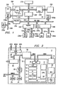
- Figure 1 illustrates a conventional microprocessor-based computer system 200, as an exemplary arrangement of a host CPU 210, the interface chipset CS, and the various buses that are used in connection with conventional computers.
- System 200 of Figure 1 is presented herein by way of example and for description purposes only, it being understood that conventional systems may be constructed with more or fewer resources than shown in Figure 1, and in various differing arrangements.
- Host CPU 210 in system 200 of Figure 1 is a conventional microprocessor as currently used in modern, high-performance, personal computers, workstations, and portable computers; for example, host CPU 210 may be an x86-architecture microprocessor of the so-called P5 or P6 class (corresponding, for example, to the PENTIUM and PENTIUM PRO microprocessors available from Intel Corporation).
- Host CPU 210 communicates with the other elements of system 200 primarily by way of host bus 212; host bus 212 operates according to the particular external bus protocol driven by host CPU 210, as known in the art.
- host bus 212 is a lightly-loaded bus, implemented with a "back-plane" of minimum length to minimize bus loading and losses and thus to maintain high speed data transfer.
- Chipset CS in system 200 of Figure 1 includes several separate integrated circuits, typically mounted on the mother board of system 200 along with host CPU 210, each providing an interface between host bus 212 and a system resource.
- chipset CS includes cache controller 214, which controls communication of data between host CPU 210 and external cache memory 216, typically implemented as high-speed static RAM, and serving as a level-2 or level-3 cache memory depending upon the internal architecture of host CPU 210.
- Chipset CS further includes main memory controller 218, which controls communication of data between host CPU 210 and main memory 220, which is typically implemented as banks of dynamic RAM.
- Chipset CS in system 200 further includes host/PCI bridge 222, which provides an interface between host bus 212 and a first-level PCI bus 224.
- PCI bus 224 is a high-speed, synchronous, bus-mastered-architecture, system bus for providing high-speed data communications among system resources.
- PCI resources 225a, 225b are illustrated as resident on first-level PCI bus 224, and represent such system resources as high-performance graphics display systems, additional expansion memory, disk storage systems, and other CPUs, in multiprocessor systems.
- PCI buses are 32-bit buses, operating at either 33 MHz or 66MHz frequencies using address and data multiplexing, with the capability of 64-bit data transfer provided by an additional level of multiplexing.
- Host/PCI bridge 222 is a conventional device known in the art for interfacing PCI bus 224 to host bus 222. In this capacity, host/PCI bridge 222 is necessarily responsible for reformatting the commands, address, and data signals communicated from one bus to another; modern implementations of host/PCI bridge 222 also contain logic to combine commands and to prefetch data, for improved system performance.
- system 200 includes PCI/ISA bridge 226 which is connected between first-level PCI bus 224 and ISA bus 228.
- ISA bus 228 has ISA resources 230a, 230b resident thereupon, such resources referred to as "legacy” resources (and ISA bus 228 as a "legacy” bus), indicating the older bus protocol with which they operate.
- PCI/ISA bridge 226, as known in the art, is a resource that reformats signals when communicated from bus-to-bus, and which may also include logic for combining commands and prefetching data.
- System 200 also includes PCI/PCI bridge 232 which interfaces first-level PCI bus 224 to two second-level PCI buses 234a, 234b, upon which PCI resources 236a, 236b are respectively resident.
- PCI/PCI bridge 232 is a known device in the art that is often referred to as a PCI "splitter", as it provides, in this example, interface control between multiple lower-level PCI buses 234 and higher-level PCI bus 224.
- PCI/PCI bridge 232 thus enlarges the number of potential PCI resources available in system 200 without unduly loading first-level PCI bus 223, and also permits PCI buses 224, 234a, 234b to operate according to different clock speeds, data widths, and logic levels, such options available under the PCI specification.
- system 200 in this example also includes PCI/CardBus bridge 240, for interfacing first level PCI bus 224 to CardBus resources 242a, 242b resident on separate CardBus buses 241a, 241b, respectively.
- CardBus buses are variants of the PCMCIA buses, and are particularly suitable for use in portable computers to implement peripherals such as disk drives, modems, and the like.
- PCI/CardBus bridge 240 is also a known device in the art, such as the PCI1130 CardBus controller available from Texas Instruments Incorporated, which interfaces PCI bus 224 to resources of either the CardBus or PCMCIA type, at either 3.3 volt or 5 volt logic levels.
- the PCI bus standard is intended to reduce the number of local bus protocols that may otherwise be generated in the marketplace.
- many different bus types are still utilized in modern personal computers, workstations, and portable computers, even within individual systems.
- the PCI bus itself has several option, including different bit widths, different bus clock rates, and different logic level standards. Accordingly the, size, speed, and protocol of expansion buses continue to proliferate in the field.
- one type of configurable bus controller component has been implemented in SparcStation 10 and SparcStation 20 workstations sold by Sun Microsystems, Inc.
- This bus controller referred to a MultiCache Controller and manufactured by Texas Instruments Incorporated under the part number TMS390Z55, is configurable in that it is selectably configured to interface a host CPU with one or the other of two mutually exclusive bus protocols.
- the invention provides a microprocessor host module for a computer system as defined in the appended claims.
- the present invention may be implemented into a microprocessor system by way of a configurable expansion bus controller that is closely integrated with the host central processing unit (CPU) of the system.
- the expansion bus controller receives a bus from the CPU on one side, and is configured, by way of control signals, to interface with a single bus, or with multiple buses of narrower bit width.
- the multiple buses may be of similar or different types, and may be driven at the same or at different bus clock frequencies.
- the present invention is preferably implemented into a closely integrated fashion, particularly relative to the proximity of certain of the functions therein.
- Methods of implementing such close integration include the integration of functions into the same integrated circuit chip (i.e., unitary semiconductor element), and also the assembly of multiple integrated circuit chips within a single integrated package so as to appear as a single integrated circuit chip to the external system.
- this close integration provides the important benefit of providing a high level of functionality with relatively low pin count, which is especially desirable considering the high cost (both system cost and device cost) of extremely large pin count devices, such as those exceeding 208 pins according to current technology.
- FIG. 2 illustrates a host central processing module 2 according to a first embodiment of the present invention, in which host module 2 represents a multi-chip module.
- multi-chip module refers to a single integrated circuit package within which two or more integrated circuit chips are implemented.
- host module 2 includes superscalar CPU 10 which is a high-performance microprocessor capable of executing sequences of program instructions upon digital data, in the conventional manner.
- CPU 10 is of the well-known x86-architecture, preferably of a capability consistent with the so-called P5 or P6 classes of microprocessor; of course, CPU 10 may be implemented according to variations upon this architecture, or according to architectures other than the x86-architecture.
- CPU 10 includes various functional circuitry of the x86 architecture type to perform a sequence of data processing instructions.
- CPU 10 is of the superscalar type, and as such is capable of issuing and executing multiple instructions in parallel, absent resource conflicts or data dependencies.
- CPU 10 includes multiple execution units 17, 18, each of which include circuitry for performing operand fetch, execution, and writeback operations by way of one or more arithmetic or logic units.
- Execution units 17, 18 may each be integer execution units, or one may be a floating-point unit and the other an integer unit; of course, additional execution units may also be implemented within CPU 10, as desired for the particular architecture.
- Load/store units 12 are included within CPU 10 to control memory access for loading instructions from, and communicating data between, internal cache memory 13 or memory external to CPU 10 as will be described hereinbelow.
- CPU 10 is of the pipelined type, and as such instruction fetch circuitry 15 and instruction decoder 16 support one or more instruction pipelines.
- Instruction decoder 16 decodes instructions fetched by fetch circuitry 15 from cache 13, or alternatively microcode instructions generated by microcode unit 11 and applied to fetch circuitry 15, into control signals communicated to and applied by control unit 14 to control the operation of CPU 10.
- CPU 10 also includes register file 20, which includes the usual named x86 architecture registers for retaining data, control, and status information.
- CPU 10 includes bus interface unit (BIU) 8 for controlling the communication of data to and from CPU 10, for example by way of module bus IBUS.
- Module bus IBUS is a bus for communicating address, data, and control signals among the various constituent blocks of host module 2.
- module bus IBUS passes through data route and bus control circuitry 25, which is circuitry that controls the traffic among the various system elements on module bus IBUS. It is contemplated that one of ordinary skill in the art will be able to realize data route and bus control circuitry 25 according to conventional techniques, as appropriate for the particular system; for example, data route and bus control circuitry 25 may be implemented as a simple crossbar, or alternatively may be implemented as a more complex bus arbiter and control circuit that does not intercept module bus IBUS.
- module bus IBUS refers to the internal module bus by way of which host CPU 10 communicates with other module elements in module 2.
- Memory controller 22 in the multi-chip module arrangement of host module 2, is an integrated circuit, constructed according to conventional techniques, which controls the communication of data to and from module bus IBUS and main module memory 24, which is preferably implemented within host module 2 as synchronous DRAM. Memory controller 22 communicates with main module memory 24, and with expansion memory connected externally to host module 2, by way of memory bus XMBUS.
- Host module 2 also may include other special system resources resident on module bus IBUS.
- host module 2 of Figure 1 includes graphics controller 26, which may be implemented as a high-performance graphics processor and adapter for performing graphics operations such as line draw, fill, bit block transfers, and the like, and for presenting the results to a graphics monitor.
- graphics controller 26 may be implemented as a high-performance graphics processor and adapter for performing graphics operations such as line draw, fill, bit block transfers, and the like, and for presenting the results to a graphics monitor.
- graphics controller 26 may be implemented as a high-performance graphics processor and adapter for performing graphics operations such as line draw, fill, bit block transfers, and the like, and for presenting the results to a graphics monitor.
- graphics controller 26 may be implemented as a high-performance graphics processor and adapter for performing graphics operations such as line draw, fill, bit block transfers, and the like, and for presenting the results to a graphics monitor.
- other elements of different types may also be included within host module 2, as desired by the system architect.
- BIU 8 of host CPU 10 is also in communication with cache memory 6 by way of cache bus CBUS, which is a separate bus from module bus IBUS in this example.
- Cache memory 6 is a level-2 or level-3 cache, depending upon the levels of cache provided within CPU 10, for locally storing data and instructions that are either recently used or likely to be used in the particular instruction sequences being executed by CPU 10.
- cache 6 may be coupled to CPU 10 by away of module bus IBUS.
- host module 2 includes on-module oscillator/synchronization circuitry 27 for generating and applying the appropriate clock signals to the resources in host module 2, and module power regulator circuit 29 for ensuring the application of the appropriate power. levels to the various resources of host module 2.
- Other conventional system control resources will also be included within host module 2, as typical in the art.
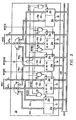
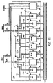
- host module 2 further includes configurable expansion bus controller 28, coupled between module bus IBUS internal to host module 2, and external buses XPCI0, XPCI1 which communicate address, data, and control signals between resources in host module 2 and external system resources.
- Buses XPCI0, XPCI1 are each capable of operating as a full 32-bit PCI bus, operating at either a low frequency (e.g., 33 MHz) or at a high frequency (e.g., 66 MHz) according to the current PCI standard; in addition, buses XPCI1, XPCI0 are capable of operating in combination with one another as a 64-bit wide PCI bus, also at either the high or low frequency.
- each of buses XPCI0, XPCI1 may operate as lower-performance buses, for example according to the CardBus standard which, as discussed above, is a 32-bit variant upon the PCMCIA bus standard for portable computer peripherals, and operates at a frequency corresponding to the low frequency of the PCI standard (e.g., 33 MHz).
- External buses XPCI1, XPCI0 include multiplexed address and data lines, and also control lines, with the names and functions of the lines specified according to the particular configuration mode. Assignment of the signal lines for buses XPCI1, XPCI0, in the modes of 64-bit PCI, 32-bit PCI, and CardBus, are as follows:
- expansion bus controller 28 configuring buses XPCI1, XPCI0 to operate in combination with one another, such that the address, data, and CBE (command/byte enable) lines of bus XPCI1 serve as the higher order address, data, and CBE lines when in the 64-bit PCI mode; in this mode, the control signals associated with bus XPCI0 serve as the control signals for the entire 64-bit bus, and as such the control signals of bus XPCI1 are not used.
- buses XPCI1, XPCI0 operate as separate 32-bit buses, either in the PCI or CardBus modes, the address, data, CBE, and control lines of each of the buses XPCI1, XPCI0 operate independently from one another.
- the configuration of buses XPCI1, XPCI0 is selected by expansion bus controller 28 in response to configuration lines BCFG from external to host module 2.
- Configuration lines BCFG are preferably power-on-time signals, for example generated merely by hardwiring external conductors on a mother board containing host module 2 to a power supply voltage or to ground.
- five configuration lines BCFG[4:0] are used to indicate the desired configuration of external buses XPCI1, XPCI0, and the operating clock frequency of each bus.
- module bus IBUS includes address/data portions A/D and control portions C, each of which are applied to bridges 30, 32, 34, 36, 38 as will now be described.
- expansion bus controller 28 includes, associated with external bus XPCI1, CardBus bridge 30 including a data portion 30d and a control portion 30c, and 32-bit PCI bridge 32 including a data portion 32d and a control portion 30c.
- expansion bus controller 28 includes 32-bit PCI bridge 32 including a data portion 36d and a control portion 36c, and CardBus bridge 38 including a data portion 38d and a control portion 38c.
- Expansion bus controller 28 further includes 64-bit PCI bridge 34, having a data portion 34d associated with both of buses XPCI1, XPCI0, and a control portion 34c associated with external bus XPCI0 only.
- Data bridge portions 30d, 32d, 34d, 36d, 38d are preferably constructed according to conventional bridge circuit techniques for effecting bidirectional data communication between their associated two buses.
- each data bridge portion 30d, 32d, 34d, 36d, 38d preferably includes a primary bus unit and a secondary bus unit assigned arbitrarily to one of the buses to which the bridge is connected.
- Each of the primary and secondary units preferably include a prefetch buffer, generally including a first-in-first-out memory (FIFO), for retrieving and temporarily storing expected data to be communicated from its associated bus (when operating as a source bus), and a posting buffer, also typically implemented as a FIFO, for receiving and temporarily storing data to be communicated to its associated bus (when serving as the destination bus).
- FIFO first-in-first-out memory
- Each of data bridge portions 30d, 32d, 34d, 36d, 38d also typically include data paths for bidirectional communication of signals between the primary and secondary units, and also the appropriate driver circuitry for applying the communicated data and address information at the appropriate logic levels.
- data bridge portions 30d, 32d, 34d, 36d, 38d may be constructed according to alternative techniques.
- data bridge portions 30d, 32d, 34d, 36d, 38d may be shared; specifically, considering that not all of data bridge portions 30d, 32d, 34d, 36d, 38d will be enabled, FIFO buffering on the module bus IBUS side may be shared among data bridge portions 30d, 32d, 34d, 36d, 38d, reducing the chip area required for expansion bus controller 28 while slightly increasing the complexity of select circuitry therewithin.
- Other realizations of data bridge portions 30d, 32d, 34d, 36d, 38d will, of course, become apparent to those of ordinary skill in the art having reference to this specification.
- Each data bridge portion 30d, 32d, 34d, 36d, 38d receives address and data lines A/D from module bus IBUS; similarly, control portions 30d, 32d, 34d, 36d, 38d each receive control lines C from module bus IBUS.
- Data bridge portions 30d, 32d, 34d are also connected to corresponding data buses 40d, 42d, 44d that are in turn connected to bidirectional multiplexer 50, with only the portion 44d 1 of data bus 44d being applied to multiplexer 50.
- data bridge portions 34d, 36d, 38d are connected to bidirectional multiplexer 52 by way of corresponding data buses 44d, 46d, 48d, with only the portion 44d 0 of data bus 44d applied to multiplexer 52.
- Bidirectional multiplexers 50, 52 may, if desired, include the appropriate input and output buffering for interfacing with external buses XPCI1, XPCI0 in the configured manner.
- command and byte enable signals i.e., the "CBE" signals according to the PCI specification
- data bridge portions 42d, 44d, 46d in combination with the address and data signals.
- each of data buses 40d, 42d, 44d 1 , 44d 0 , 46d, 48d include at least thirty-two address/data lines and four CBE lines, as necessary for PCI operation.
- Bidirectional multiplexer 50 selects one of buses 40d, 42d, 44d 1 for bidirectional communication with address/data lines A/D 1 of external bus XPCI1, while bidirectional multiplexer 52 selects . one of buses 44d 0 , 46d, 48d for bidirectional communication with address/data lines A/D 0 of external bus XPCI0.
- the selection performed by multiplexers 50, 52 is controlled by the states of control lines BCFG[2:0], which are a subset of configuration lines BCFG.
- Bidirectional multiplexers 50, 52 may be constructed according to the conventional manner for such circuit functions, for example as pass-gate multiplexers to allow data to flow in either direction.
- the multiplexer function may be merely performed by wired-OR connection of the corresponding data buses (i.e., buses 40d, 42d, 44d 1 wired together, and buses 44d 0 , 46d, 48d wired together), assuming that the data bridge portions associated with non-selected buses are controlled so as to have their corresponding buses in a high-impedance state.
- Each of control bridge portions 30c, 32c, 34c, 36c, 38c have a select input SEL that is controlled according to the state of configuration lines BCFG[2:0] in this example, in a manner consistent with the selections made by multiplexers 50, 52 as indicated in the above truth table.
- select input SEL of CardBus control bridge 30c receives the output of AND function 54, which receives the logical complement of configuration line BCFG[2] and the true state of configuration line BCFG[1].
- Select input SEL of 32-bit PCI control bridge 32c receives the output of AND function 56, which receives the logical complements of configuration lines BCFG[1] and BCFG[2] at its inputs.
- Select input SEL of 64-bit PCI control bridge 32c simply receives the state of configuration line BCFG[2].
- Select input SEL of 32-bit PCI control bridge 36c receives the output of AND function 60, which receives the logical complements of configuration lines BCFG[2] and BCFG[0] at its inputs.
- select input SEL of CardBus control bridge 38c receives the output of AND function 62, which receives the logical complement of configuration line BCFG[2] and the true state of configuration line BCFG[0] at its inputs.
- This logic arrangement thus corresponds to the truth table for multiplexers 50, 52 noted hereinabove.
- control bridge portions 30c, 32c receive control signal lines C from module bus IBUS, and generate the corresponding control signals on control buses 40c, 42c, respectively, according to the associated CardBus and PCI standard, respectively.
- control bridge portions 34c, 36c, 38c receive control signal lines C from module bus IBUS, and generate the corresponding control signals on control buses 44c, 46c, 48c for their associated buses.
- control buses 40c, 42c are wired-OR connected with one another to form the control signal portion C 1 of external bus XPCI1
- control buses 44c, 46c, 48c are wired-OR connected with one another to form the control signal portion C 0 of external bus XPCI0.
- each control bridge portion 30c, 32c 34c, 36c, 38c places its associated control bus 40c, 42c, 44c, 46c, 48c into a high-impedance state when unselected by configuration lines BCFG[2:0].
- each of PCI bridges 32, 34, 36 are capable of generating address, data, and control signals for application to the external buses XPCI1, XPCI0 in either high-frequency or low-frequency mode, according to the state of the signal applied to their clock control input HS.
- the high-frequency mode corresponds to 66 MHz
- the low-frequency mode corresponds to 33 MHz; of course, the specific bus clock frequencies will depend upon the particular prevailing industry standards, typically limited by the speed of the external resources to which the external buses XPCI1, XPCI0 are connected.
- 64-bit PCI bridge 34 operates in high-frequency mode if both of configuration signals BCFG[4:3] are at a low logic level, and as such input HS of control bridge 34c receives the output of NOR function 58, which receives configuration signals BCFG[4:3] at its inputs.
- the inputs HS of 32-bit control bridge portions 32c, 36c receive the logical complement of configuration lines BCFG[4], BCFG[3], respectively, such that the state of these configuration lines BCFG[4:3] independently control the frequency of operation of buses XPCI1, XPCI0 when in 32-bit PCI modes.
- CardBus control bridges 30c, 38c are only capable of low-frequency operation, and as such have no inputs HS associated therewith.
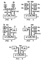
- configurable expansion bus controller 28 may configure external buses XPCI1, XPCI0 in various ways, depending upon the state of configuration lines BCFG[4:0] which, as noted above, are preferably set at power-on time simply by hardwiring to the desired voltage levels on the mother board containing host module 2. Examples of the various system implementations available will now be described relative to Figures 4a through 4e, in combination with Figure 3.
- Figure 4 illustrates the case where expansion bus controller 28 is placed into 64-bit PCI mode. As described hereinabove, this mode is selected by configuration line BCFG[2] being at a high logic level; the state of configuration lines BCFG[1:0] are don't cares in this mode. In this mode, referring back to Figure 3, 64-bit PCI bridge 34 is selected, and all other bridges 30, 32, 36, 38 are deselected. Address/data lines A/D of internal bus IBUS are thus placed in bidirectional communication with address/data lines A/D 1 of external bus XPCI1 (as the higher-order lines in the 64-bit PCI bus), and with address/data lines A/D 0 of external bus XPCI0 (as the lower-order lines in the PCI bus).
- Control lines C of module bus IBUS are used, by control bridge portion 34c, to generate the appropriate control signals for PCI bus operation, as applied to control lines C 0 of external bus XPCI0; control lines C 1 of bus XPCI1 are in a high-impedance state (bridges 30, 32 both deselected); conversely, control signals from control lines C 0 of bus XPCI0 are communicated by control bridge portion 34c to module bus IBUS, as necessary.
- the frequency at which expansion bus controller 28 operates is determined by the states of configuration lines BCFG[4:3], as described hereinabove. If either of configuration lines BCFG[4:3] are high, control bridge portion 34c will cause operation to be in low-frequency mode; if neither are high, control bridge portion 34c will operate in the high-frequency mode, which is contemplated to be on the order of 66 MHz.
- FIG. 4 illustrates a system . implementation of this configuration of expansion bus controller 28.
- buses XPCI1, XPCI0 cooperatively form a 64-bit PCI bus 64, upon which PCI resources 66a, 66b that are capable of 64-bit PCI protocol communication with host module 2 (which includes host CPU 10, as described above) may reside.
- PCI resources 66a, 66b that are capable of 64-bit PCI protocol communication with host module 2 (which includes host CPU 10, as described above) may reside.
- PCI resources 66a, 66b may reside on bus 64; in fact, it is contemplated that a PCI bus "splitter" (i.e., PCI/PCI bridge) may itself reside on bus 64, providing further hierarchical bus arrangements of PCI resources.
- splitter i.e., PCI/PCI bridge
- Figure 5 illustrates the case where expansion bus controller 28 is configured to drive two 32-bit PCI buses. This configuration is selected by configuration lines BCFG[2:0] being all low.
- 32-bit PCI bridge 32 is selected, such that data bus 42d is selected for communication with bus XPCI1 through bidirectional multiplexer 50 and control lines 42c are activated for application to bus XPCI1;
- 32-bit PCI bridge 36 is also selected, so that data bus 46d is selected for communication with bus XPCI0 through bidirectional multiplexer 52, and so that control lines 46c are activated for application to bus XPCI0. All other bridges 30, 34, 38 in expansion bus controller 28 are deselected in this case.
- the system of Figure 4b may be provided in this configuration, where 32-bit PCI resources 68a, 68b are resident upon bus XPCI1, and where 32-bit PCI resources 70a, 70b are resident upon bus XPCI0.
- buses XPCI1, XPCI0 may be at different frequencies from one another, or at the same frequency, depending primarily upon the capabilities of the resources 68, 70 attached thereto. Particularly if additional configuration lines are provided, it is contemplated that other options, such as selectable logic levels (e.g., 5 volt versus 3.3 volt), may be independently selected for use in connection with buses XPCI1, XPCI0. Accordingly, expansion bus controller 28 provides system flexibility, even where buses XPCI1, XPCI0 are configured as separate 32-bit PCI buses.
- FIG. 6 illustrates a system according to another configuration of expansion bus controller 28.
- bus XPCI1 is configured as a 32-bit PCI bus
- bus XPCI0 is configured as a CardBus bus.
- PCI resources 72a, 72b reside on bus XPCI1
- CardBus resource 74 resides on bus XPCI0.
- a single resource or, conceivably, a bus "splitter”
- multiple CardBus resources 74 could then reside on bus XPCI0.
- the configuration of Figure 4c is selected by configuration lines BCFG[2:0] being in the 001 state, selecting 32-bit PCI bridge 32 and CardBus bridge 38 in expansion bus controller 28 (along with multiplexers 50, 52 selecting their corresponding data buses 42d, 48d), and deselecting bridges 30, 34, 36.
- the state of configuration line BCFG[4] determines whether bus XPCI1 operates at a high or low frequency. Since the CardBus standard, in this example, is only a low-frequency bus, no frequency selection is provided in this situation, and line BCFG[3] is thus a don't care.
- Figure 7 illustrates the converse situation from that of Figure 6, in which bus XPCI1 is configured as a CardBus bus and bus XPCI0 is configured as a 32-bit PCI bus, due to configuration lines BCFG[2:0] being at the 010 state.
- Bus XPCI0 may be in either the high or low frequency mode, as indicated by configuration line BCFG[3].
- CardBus resource 76 is resident upon bus XPCI1
- 32-bit PCI resources are resident on bus XPCI0.
- bridges 30, 36 of expansion bus controller 28 are selected, and their respective data buses 40d, 46d selected by bidirectional multiplexers 50, 52, respectively; bridges 32, 34, 38 are deselected.
- expansion bus controller 28 according to the preferred embodiment of the invention is capable of being configured to communicate with buses of different types; in this example, the high-speed high-performance PCI bus and the lower performance CardBus bus. Further, expansion bus controller 28 may operate these buses at different frequencies, also readily configurable such as by way of hardwired configuration lines BCFG[4:3].
- expansion bus controller 28 is configured so that both of buses XPCI1, XPCI0 are CardBus buses. This configuration is selected by configuration lines BCFG[2:0] set to the state 011; since CardBus operation is only at low frequency, the state of configuration lines BCFG[4:3] are both don't cares.
- CardBus resources 80, 82 in this example, are resident on buses XPCI1, XPCI0, respectively.
- bridges 30, 38 are both selected, and their data buses 40d, 48d selected by bidirectional multiplexers 50, 52, respectively.
- Control bridges 30c, 38c each generate and receive CardBus protocol control signals from buses XPCI1, XPCI0, for communication with module bus IBUS in the appropriate manner.
- expansion bus controller 28 is constructed with separate data and control bridges for each bus mode (PCI, CardBus) for each output bus (XPCI1, XPCI0). It has been discovered, in connection with another embodiment of the present invention, that the frequency at which module bus IBUS and host CPU 10 operate is typically many times faster than the frequency at which bus traffic occurs, even for high performance buses such as the 64-bit 66MHz PCI bus. This differential in operating frequencies is used to advantage according to another embodiment of the invention, as will now be described relative to Figure 5.
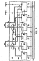
- Figure 9 illustrates expansion bus controller 28' according to a second embodiment of the present invention. Like elements in expansion bus controller 28' illustrated in Figure 9 to those in expansion bus controller 28 illustrated in Figure 3, are referred to by the same reference numerals.
- five data bridges 30d, 32d, 34d, 36d, 38d are provided as before, for controlling communication between corresponding data buses 40d, 42d, 44d, 46d, 48d and address/data lines A/D of module bus IBUS, as before.
- Data buses 40d, 42d, 44d, 46d, 48d are applied to bidirectional multiplexers 50, 52, in the same manner as in configurable expansion bus controller 28 of Figure 3; multiplexers 50, 52 select among these data buses for application to address/data lines A/D of external buses XPCI1, XPCI0, responsive to the states of configuration lines BCFG[2:0].
- bridges 30d, 38d are CardBus bridges associated with buses XPCI1, XPCI0, respectively;
- bridges 32d, 36d are 32-bit PCI bridges associated with buses XPCI1, XPCI0, respectively; and bridge 34d is a 64-bit PCI bridge associated with both of buses XPCI1, XPCI0.
- Each of bridges 30d, 32d, 34d, 36d, 38d have a select decoder input SEL DEC, which receives configuration lines BCFG[2:0 ⁇ , according to which each bridge 30d, 32d, 34d, 36d, 38d determines whether or not it is selected, for example according to the same truth table as described hereinabove for expansion bus controller 28 of Figure 3.
- a single time-multiplexing bus control 84 is provided, for generating the desired bidirectional control signals associated with control buses C 1 , C 0 of buses XPCI1, XPCI0, respectively.
- Bus control 84 receives (and applies) control signals to control lines C of module bus IBUS as well, to effect bidirectional communication between buses XPCI1, XPCI0 and module bus IBUS.
- Time-multiplexing bus control 84 may be realized as sequential logic, for example by way of two separate state machines, for generating and receiving the appropriate control signals from either side. Because of the much higher rate at which address, data, and control signals are generated by host CPU 10 and other resident resources on module bus IBUS, it is contemplated that, through use of conventional sequential logic bus control 84 could readily be realized to generate the appropriate bus control signals, in any of the 64-bit PCI bus, 32-bit PCI bus, and CardBus modes (and combinations thereof, as described hereinabove relative to Figures 4a through 4e), in a time-multiplexed manner.
- Control signal mode for buses XPCI1, XPCI0, according to which bus control 84 is to operate, is determined from the state of configuration lines BCFG[2:0] applied to decode input DEC of bus control 84.
- Frequency configuration is selected according to the state of configuration lines BCFG[4:3], which are applied to input SPD of bus control 84.
- Bus control 84 for example according to the truth tables described hereinabove relative to expansion bus controller 28, includes decode circuitry for determining the states of configuration lines BCFG[4:0] and for controlling the sequential logic therein in the appropriate manner for generating the necessary control lines on buses XPCI1, XPCI0, and IBUS.
- Figures 3 and 9 are intended to illustrate alternative implementations of the expansion bus controller according to the' present invention, including a time-multiplexed implementation and a non-time multiplexed (i.e., a spatially-multiplexed) version. It is contemplated that those of ordinary skill in the art having reference to this specification may readily implement this functionality according to alternative approaches and combinations of time-multiplexing and spatial-multiplexing, without departure from the present invention. It is contemplated that one such alternative approach would include the further consolidation of the data bridge functions relative to Figures 3 and 9, for example by providing shared buffers on the host side of the expansion bus controller.
- FIG 10 illustrates host CPU chip 10' which, in this example, is also an x86-architecture microprocessor such as that of the P5 or P6 class; accordingly, many of the same internal elements of CPU 10' pertaining to the fetching and execution of instructions, are identical to those described hereinabove relative to Figure 1.
- CPU 10' according to this embodiment of the invention also includes, however, on the same integrated circuit chip, memory controller 22' and configurable expansion bus controller 28'', for effecting communication with external resources.
- Memory controller 22' is connected to internal bus INTBUS, primarily to on-chip cache 13 and load/store units 12, for controlling access to external memory, including external cache memory 6 and main memory 86, both by way of memory bus MBUS. Such memory access will be effected in the event of a cache miss (relative to cache 13), or for non-cacheable reads and writes via load/store units 12, in the usual manner.
- Memory controller 22' thus may operate as a bus master on internal bus INTBUS, controlling memory accesses according to the desired protocol.
- Configurable expansion bus controller 28'' in this example is also connected to internal bus INTBUS, and controls communication with external resources via buses XPCI1, XPCI0, in the manner described hereinabove.
- expansion bus controller 28'' is preferably determined by the state of configuration lines BCFG[4:0], for example in the manner described hereinabove.
- expansion bus controller 28" may be configured to operate buses XPCI1, XPCI0 as a single 64-bit PCI bus (at either high or low frequencies), or as separate buses of the same or different types, such as according to the 32-bit PCI bus and CardBus protocols, again at the same or different clock frequencies, logic levels and the like.
- the benefits of configurable expansion buses are obtained in a single-chip CPU, where the expansion bus controller is realized on the same chip as other host CPU functions.
- This single-chip integration is enabled by the functionality of the expansion bus controller according to the present invention that provides a wide range of flexibility in the configuration of the external buses, including bit width, clock frequency, logic levels, and other options.
- expansion bus controller 128 includes data bridges 30d, 32d, 34d associated with external bus XPCI1, and data bridges 34d, 36d, 38d associated with external bus XPCI0, all coupled to lines A/D of module bus IBUS as before.
- expansion bus controller 128 also includes AGP 1X data bridge 31d and AGP 2X data bridge 33d, both coupled to lines A/D of module bus IBUS and associated with external bus XPCI1, and AGP 1X data bridge 37d and AGP 2X data bridge 39d, both coupled to lines A/D of module bus IBUS and associated with external bus XPCI0.
- AGP 1X data bridges 31d, 37d are configured as bridge circuitry for communicating data between module bus IBUS and address/data buses 41d, 47d, respectively, according to the well-known AGP standard, with data transferred once per bus cycle (e.g., on the rising edge of the bus clock).
- AGP 2X data bridges 33d, 39d communicate data between module bus IBUS and address/data buses 43d, 49d, respectively, also according to the AGP bus standard but with two data transfers per cycle (e.g., one transfer on the bus clock rising edge and another transfer on the bus clock falling edge).
- Expansion bus controller 128 includes bidirectional multiplexers 150, 152, for selecting among the associated data bridge circuitry to be placed in communication with lines A/D 1 , A/D 0 of external buses XPCI1, XPCI0, respectively.
- Bidirectional multiplexers 150, 152 effect such selection in response to the state of five configuration signals BCFG[4:0], in the manner to be described hereinbelow.
- buses 40d, 41d, 42d, 43d, and 44d 1 are applied to bidirectional multiplexer 150, while buses 44d 0 , 46d, 47d, 48d, 49d are applied to bidirectional multiplexer 152.
- buses 44d 1 , 44d 0 respectively correspond to the upper and lower order portions at the output of 64 bit PCI data bridge 34d.
- Each of data bridges 30d, 31d, 32, 33, 34, 336d, 37d, 38d, 39d have select inputs that receive the state of corresponding ones of configuration signals BCFG[4:0]; alternatively, decode circuitry may be provided externally to the data bridges to generate individual select signals.
- seven configuration signals BCFG[6:0] are received by expansion bus controller 128, the lower order five of which (BCFG[4:0]) configure the selection of the appropriate bus protocol or protocols for external buses XPCI1, XPCI0.
- configuration signal BCFG[4] when asserted, enables 64 bit PCI data bridge 34d to communicate address, data and byte enable signals and controls multiplexers 150, 152 to select data buses 44d 1 , 44d 0 , respectively.
- configuration signals BCFG[4:2] in combination, control the enabling of data bridges 30d, 31d, 32d, 33d, and 34d, and the corresponding selection by bidirectional multiplexer 150 as follows: BCFG[4:2] Data bridge selected XPCI1 Configuration 1XX 34d Upper 32 bits of 64-bit PCI 000 32d 32-bit PCI 001 30d CardBus 010 31d 32-bit AGP (1X) 011 33d 32-bit AGP (2X)
- configuration signals BCFG[4, 1:0] control the enabling of data bridges 34d, 36d, 37d, 39d and the selection made by bidirectional multiplexer 152, according to the following table: BCFG[4, 1:0] Data bridge selected XPCI0 Configuration 1XX 34d Lower 32 bits of 64-bit PCI 000 36d 32-bit PCI 001 38d CardBus 010 37d 32-bit AGP (1X) 011 39d 32-bit AGP (2X)
- Control bridge 90 in expansion bus controller 128 communicates control signals between control lines C of module bus IBUS and control buses C 1 , C 0 of external buses XPCI1, XPCI0, respectively, as before, and also the bus clock frequency to be used, responsive to configuration signals BCFG[6:0], as will now be described relative to Figure 12.
- control bridge 90 includes control bridge portions 30c, 31c, 32c, associated with control lines C 1 of external bus XPCI1, and control bridge portions 34c, 36c, 38c, 37c associated with control lines C 0 of external bus XPCI0.
- AGP control bridge portion 31c is associated with both of AGP data bridges 31d, 33d, and as such generates and receives control signals associated with the AGP bus protocol, in both the 1X and 2X modes; similarly, AGP control bridge portion 37c is associated with both of AGP data bridges 37d, 39d for the same function.
- control bridge portions 30c, 31c, 32c, 34c, 36c, 37c, 38c have a select input S receiving a decoded select signal from configuration logic 92.
- Configuration logic 90 receives configuration signals BCFG[6:0], and generates decoded select signals applied to select signals S according to the truth tables given hereinabove for the corresponding data portions.
- AGP control bridge 31c is selected when either of data bridges 31d, 33d are selected; similarly, AGP control bridge 37c is selected when either of data bridges 37d, 39d are selected.
- some of the available bus protocols may be operable in expansion bus controller 128 in both a high frequency and a low frequency mode.
- the high frequency mode may operate. with a bus clock of 66 MHz
- the low frequency mode may operate with a 33 MHz bus clock rate; the particular frequencies utilized as the high and low frequency modes may differ from these exemplary values, of course, depending upon the prevailing bus standards.
- control bridge portions 31c, 32c, 34c thus have a high-speed input HS connected to control line BC1 generated by configuration logic 92 in response to configuration signal BCFG[6]; conversely, control bridge portions 36c, 37c also have a high-speed input connected to receive control line BC0, generated by configuration logic 92 responsive to configuration signal BCFG[5].
- Control bridge portions 30c, 38c have no high-speed control inputs, as they can only operate at the lower bus clock frequency.
- the truth table for selecting the bus frequencies of the selected control bridge portions may be as follows: BCFG[6:5] XPCI1 Frequency XPCI0 Frequency 00 High High 01 High Low 10 Low High 11 Low Low Low
- control line BC1 controls the bus speed in 64-bit PCI mode (i.e., control line BC0 is don't care in this condition, as illustrated in Figure 12).
- control line BC0 is don't care in this condition, as illustrated in Figure 12.
- an additional bus in this example the AGP bus
- this bus protocol can include selectable data transfer rates, including multiple data transfers per cycle.
- 2X data transfer modes may also be realized in the 64-bit and 32-BIT PCI standards, and in other standards.
- other bus protocol types either legacy or otherwise may be utilized in connection with the present invention.
- the present invention enables the combination of multiple buses into a single wider bus when desired for system implementation, and also enables the communication with multiple buses of the same type, or of different type, depending upon the system architecture. It is therefore contemplated that the present invention will provide great flexibility in system implementation, while still obtaining high bus communication performance, and at reduced pin count and thus reduced system and device cost.
Landscapes
- Engineering & Computer Science (AREA)
- Theoretical Computer Science (AREA)
- General Engineering & Computer Science (AREA)
- Physics & Mathematics (AREA)
- General Physics & Mathematics (AREA)
- Computer Hardware Design (AREA)
- Bus Control (AREA)
- Information Transfer Systems (AREA)
- Automotive Seat Belt Assembly (AREA)
Applications Claiming Priority (2)
| Application Number | Priority Date | Filing Date | Title |
|---|---|---|---|
| US3026096P | 1996-10-31 | 1996-10-31 | |
| US30260P | 1996-10-31 |
Publications (2)
| Publication Number | Publication Date |
|---|---|
| EP0859320A1 EP0859320A1 (en) | 1998-08-19 |
| EP0859320B1 true EP0859320B1 (en) | 2003-05-02 |
Family
ID=21853337
Family Applications (1)
| Application Number | Title | Priority Date | Filing Date |
|---|---|---|---|
| EP97118807A Expired - Lifetime EP0859320B1 (en) | 1996-10-31 | 1997-10-29 | A configurable expansion bus controller |
Country Status (4)
| Country | Link |
|---|---|
| US (1) | US6085269A (cg-RX-API-DMAC7.html) |
| EP (1) | EP0859320B1 (cg-RX-API-DMAC7.html) |
| JP (1) | JPH10214250A (cg-RX-API-DMAC7.html) |
| DE (1) | DE69721474T2 (cg-RX-API-DMAC7.html) |
Families Citing this family (31)
| Publication number | Priority date | Publication date | Assignee | Title |
|---|---|---|---|---|
| US6134622A (en) * | 1995-12-27 | 2000-10-17 | Intel Corporation | Dual mode bus bridge for computer system |
| US5857086A (en) * | 1997-05-13 | 1999-01-05 | Compaq Computer Corp. | Apparatus method and system for peripheral component interconnect bus using accelerated graphics port logic circuits |
| US6481629B1 (en) * | 1997-10-17 | 2002-11-19 | I-O Data Device, Inc. | PC card with variable width data bus communication capabilities |
| US6167476A (en) * | 1998-09-24 | 2000-12-26 | Compaq Computer Corporation | Apparatus, method and system for accelerated graphics port bus bridges |
| US6249831B1 (en) * | 1999-01-29 | 2001-06-19 | Adaptec, Inc. | High speed RAID cache controller using accelerated graphics port |
| JP3895071B2 (ja) * | 1999-03-12 | 2007-03-22 | インターナショナル・ビジネス・マシーンズ・コーポレーション | バス・ブリッジ回路、情報処理システム、及びカードバス・コントローラ |
| US6581115B1 (en) * | 1999-11-09 | 2003-06-17 | International Business Machines Corporation | Data processing system with configurable memory bus and scalability ports |
| US6535939B1 (en) | 1999-11-09 | 2003-03-18 | International Business Machines Corporation | Dynamically configurable memory bus and scalability ports via hardware monitored bus utilizations |
| US6724390B1 (en) * | 1999-12-29 | 2004-04-20 | Intel Corporation | Allocating memory |
| US7107383B1 (en) * | 2000-05-03 | 2006-09-12 | Broadcom Corporation | Method and system for multi-channel transfer of data and control information |
| US6789154B1 (en) * | 2000-05-26 | 2004-09-07 | Ati International, Srl | Apparatus and method for transmitting data |
| US7162554B1 (en) * | 2001-07-11 | 2007-01-09 | Advanced Micro Devices, Inc. | Method and apparatus for configuring a peripheral bus |
| JP2006529072A (ja) * | 2003-05-20 | 2006-12-28 | コーニンクレッカ フィリップス エレクトロニクス エヌ ヴィ | 二重チャネルネットワークの同期化に関する時間トリガ型通信システムおよび方法 |
| US8788996B2 (en) * | 2003-09-15 | 2014-07-22 | Nvidia Corporation | System and method for configuring semiconductor functional circuits |
| US8732644B1 (en) | 2003-09-15 | 2014-05-20 | Nvidia Corporation | Micro electro mechanical switch system and method for testing and configuring semiconductor functional circuits |
| US8775997B2 (en) | 2003-09-15 | 2014-07-08 | Nvidia Corporation | System and method for testing and configuring semiconductor functional circuits |
| US8711161B1 (en) | 2003-12-18 | 2014-04-29 | Nvidia Corporation | Functional component compensation reconfiguration system and method |
| US8723231B1 (en) | 2004-09-15 | 2014-05-13 | Nvidia Corporation | Semiconductor die micro electro-mechanical switch management system and method |
| US8711156B1 (en) | 2004-09-30 | 2014-04-29 | Nvidia Corporation | Method and system for remapping processing elements in a pipeline of a graphics processing unit |
| US7483422B2 (en) * | 2005-02-10 | 2009-01-27 | International Business Machines Corporation | Data processing system, method and interconnect fabric for selective link information allocation in a data processing system |
| US8021193B1 (en) | 2005-04-25 | 2011-09-20 | Nvidia Corporation | Controlled impedance display adapter |
| US7793029B1 (en) | 2005-05-17 | 2010-09-07 | Nvidia Corporation | Translation device apparatus for configuring printed circuit board connectors |
| US7788420B2 (en) * | 2005-09-22 | 2010-08-31 | Lsi Corporation | Address buffer mode switching for varying request sizes |
| US8417838B2 (en) * | 2005-12-12 | 2013-04-09 | Nvidia Corporation | System and method for configurable digital communication |
| US8412872B1 (en) * | 2005-12-12 | 2013-04-02 | Nvidia Corporation | Configurable GPU and method for graphics processing using a configurable GPU |
| US8724483B2 (en) * | 2007-10-22 | 2014-05-13 | Nvidia Corporation | Loopback configuration for bi-directional interfaces |
| US8687639B2 (en) * | 2009-06-04 | 2014-04-01 | Nvidia Corporation | Method and system for ordering posted packets and non-posted packets transfer |
| US9176909B2 (en) | 2009-12-11 | 2015-11-03 | Nvidia Corporation | Aggregating unoccupied PCI-e links to provide greater bandwidth |
| US9331869B2 (en) * | 2010-03-04 | 2016-05-03 | Nvidia Corporation | Input/output request packet handling techniques by a device specific kernel mode driver |
| US9330031B2 (en) | 2011-12-09 | 2016-05-03 | Nvidia Corporation | System and method for calibration of serial links using a serial-to-parallel loopback |
| CN106130859A (zh) * | 2016-06-23 | 2016-11-16 | 北京东土科技股份有限公司 | 一种工业互联网现场层宽带总线配置管理实现方法 |
Family Cites Families (9)
| Publication number | Priority date | Publication date | Assignee | Title |
|---|---|---|---|---|
| US4534011A (en) * | 1982-02-02 | 1985-08-06 | International Business Machines Corporation | Peripheral attachment interface for I/O controller having cycle steal and off-line modes |
| US4509113A (en) * | 1982-02-02 | 1985-04-02 | International Business Machines Corporation | Peripheral interface adapter circuit for use in I/O controller card having multiple modes of operation |
| US4604683A (en) * | 1984-12-10 | 1986-08-05 | Advanced Computer Communications | Communication controller using multiported random access memory |
| GB2252432B (en) * | 1991-02-01 | 1994-09-28 | Intel Corp | Method and apparatus for operating a computer bus using selectable clock frequencies |
| US5553245A (en) * | 1994-05-11 | 1996-09-03 | Macronix International Co., Ltd. | Automatic configuration of multiple peripheral interface subsystems in a computer system |
| US5828877A (en) * | 1994-07-14 | 1998-10-27 | Dell Usa, L.P. | Circuit and method for optimizing creation of a compressed main memory image |
| US5617572A (en) * | 1995-01-31 | 1997-04-01 | Dell Usa, L.P. | System for reducing power consumption in computers |
| US5926404A (en) * | 1995-05-23 | 1999-07-20 | Dell Usa, L.P. | Computer system with unattended operation power-saving suspend mode |
| US5881247A (en) * | 1995-11-30 | 1999-03-09 | Allen-Bradley Company Llc | System having a plurality of frame bytes capable of identifying addressed recipients and assert a busy signal onto the backplane bus to forthrightly abort the message transfer |
-
1997
- 1997-10-29 DE DE69721474T patent/DE69721474T2/de not_active Expired - Lifetime
- 1997-10-29 EP EP97118807A patent/EP0859320B1/en not_active Expired - Lifetime
- 1997-10-31 JP JP9301181A patent/JPH10214250A/ja active Pending
- 1997-10-31 US US08/961,789 patent/US6085269A/en not_active Expired - Lifetime
Also Published As
| Publication number | Publication date |
|---|---|
| EP0859320A1 (en) | 1998-08-19 |
| US6085269A (en) | 2000-07-04 |
| DE69721474T2 (de) | 2004-04-08 |
| JPH10214250A (ja) | 1998-08-11 |
| DE69721474D1 (de) | 2003-06-05 |
Similar Documents
| Publication | Publication Date | Title |
|---|---|---|
| EP0859320B1 (en) | A configurable expansion bus controller | |
| US7024510B2 (en) | Supporting a host-to-input/output (I/O) bridge | |
| JP3955305B2 (ja) | 縮小命令セット・コンピュータ・マイクロプロセッサーの構造 | |
| US5911051A (en) | High-throughput interconnect allowing bus transactions based on partial access requests | |
| US7146510B1 (en) | Use of a signal line to adjust width and/or frequency of a communication link during system operation | |
| EP1750205B1 (en) | Flexible width data protocol | |
| US5826093A (en) | Dual function disk drive integrated circuit for master mode and slave mode operations | |
| US6212620B1 (en) | Single-chip microcomputer operable in master and slave modes and having configurable bus control terminals | |
| US7000092B2 (en) | Heterogeneous multi-processor reference design | |
| US6148357A (en) | Integrated CPU and memory controller utilizing a communication link having isochronous and asynchronous priority modes | |
| JP2002049576A (ja) | チップ搭載システムのためのバス・アーキテクチャ | |
| US7165133B2 (en) | Multiprocessor system having shared buses, prioritized arbitration, and clock synchronization circuitry | |
| US6317803B1 (en) | High-throughput interconnect having pipelined and non-pipelined bus transaction modes | |
| JPH08180013A (ja) | コンピュータシステム、pciバスクロック信号周波数における変化に応答してpciバス装置のコンフィギュレーションレジスタを再構成する方法、およびpciバス装置がpciバスと異なる動作速度を有することをオペレータに通知する方法 | |
| US20060195625A1 (en) | Unified USB OTG controller | |
| US6801970B2 (en) | Priority transaction support on the PCI-X bus | |
| US5963721A (en) | Microprocessor system with capability for asynchronous bus transactions | |
| US7062577B2 (en) | AMBA slave modular bus interfaces | |
| US6742058B2 (en) | Memory controller having a multiplexer selecting either second set of input signals or converted signals from first set of input signals by a bus mode input | |
| US6052754A (en) | Centrally controlled interface scheme for promoting design reusable circuit blocks | |
| US7720636B1 (en) | Performance monitors (PMs) for measuring performance in a system and providing a record of transactions performed | |
| US7711907B1 (en) | Self aligning state machine | |
| US20050278510A1 (en) | Pseudo register file write ports | |
| US8219736B2 (en) | Method and apparatus for a data bridge in a computer system | |
| US6122696A (en) | CPU-peripheral bus interface using byte enable signaling to control byte lane steering |
Legal Events
| Date | Code | Title | Description |
|---|---|---|---|
| PUAI | Public reference made under article 153(3) epc to a published international application that has entered the european phase |
Free format text: ORIGINAL CODE: 0009012 |
|
| AK | Designated contracting states |
Kind code of ref document: A1 Designated state(s): DE FR GB IT NL |
|
| AX | Request for extension of the european patent |
Free format text: AL;LT;LV;RO;SI |
|
| 17P | Request for examination filed |
Effective date: 19990219 |
|
| AKX | Designation fees paid |
Free format text: DE FR GB IT NL |
|
| RBV | Designated contracting states (corrected) |
Designated state(s): DE FR GB IT NL |
|
| 17Q | First examination report despatched |
Effective date: 20010924 |
|
| GRAH | Despatch of communication of intention to grant a patent |
Free format text: ORIGINAL CODE: EPIDOS IGRA |
|
| GRAH | Despatch of communication of intention to grant a patent |
Free format text: ORIGINAL CODE: EPIDOS IGRA |
|
| GRAA | (expected) grant |
Free format text: ORIGINAL CODE: 0009210 |
|
| AK | Designated contracting states |
Designated state(s): DE FR GB IT NL |
|
| PG25 | Lapsed in a contracting state [announced via postgrant information from national office to epo] |
Ref country code: NL Free format text: LAPSE BECAUSE OF FAILURE TO SUBMIT A TRANSLATION OF THE DESCRIPTION OR TO PAY THE FEE WITHIN THE PRESCRIBED TIME-LIMIT Effective date: 20030502 Ref country code: IT Free format text: LAPSE BECAUSE OF FAILURE TO SUBMIT A TRANSLATION OF THE DESCRIPTION OR TO PAY THE FEE WITHIN THE PRE;WARNING: LAPSES OF ITALIAN PATENTS WITH EFFECTIVE DATE BEFORE 2007 MAY HAVE OCCURRED AT ANY TIME BEFORE 2007. THE CORRECT EFFECTIVE DATE MAY BE DIFFERENT FROM THE ONE RECORDED.SCRIBED TIME-LIMIT Effective date: 20030502 |
|
| REG | Reference to a national code |
Ref country code: GB Ref legal event code: FG4D |
|
| REF | Corresponds to: |
Ref document number: 69721474 Country of ref document: DE Date of ref document: 20030605 Kind code of ref document: P |
|
| NLV1 | Nl: lapsed or annulled due to failure to fulfill the requirements of art. 29p and 29m of the patents act | ||
| PLBE | No opposition filed within time limit |
Free format text: ORIGINAL CODE: 0009261 |
|
| STAA | Information on the status of an ep patent application or granted ep patent |
Free format text: STATUS: NO OPPOSITION FILED WITHIN TIME LIMIT |
|
| ET | Fr: translation filed | ||
| 26N | No opposition filed |
Effective date: 20040203 |
|
| PGFP | Annual fee paid to national office [announced via postgrant information from national office to epo] |
Ref country code: GB Payment date: 20120925 Year of fee payment: 16 |
|
| PGFP | Annual fee paid to national office [announced via postgrant information from national office to epo] |
Ref country code: FR Payment date: 20121010 Year of fee payment: 16 Ref country code: DE Payment date: 20121031 Year of fee payment: 16 |
|
| GBPC | Gb: european patent ceased through non-payment of renewal fee |
Effective date: 20131029 |
|
| REG | Reference to a national code |
Ref country code: DE Ref legal event code: R119 Ref document number: 69721474 Country of ref document: DE Effective date: 20140501 |
|
| PG25 | Lapsed in a contracting state [announced via postgrant information from national office to epo] |
Ref country code: GB Free format text: LAPSE BECAUSE OF NON-PAYMENT OF DUE FEES Effective date: 20131029 |
|
| REG | Reference to a national code |
Ref country code: FR Ref legal event code: ST Effective date: 20140630 |
|
| PG25 | Lapsed in a contracting state [announced via postgrant information from national office to epo] |
Ref country code: FR Free format text: LAPSE BECAUSE OF NON-PAYMENT OF DUE FEES Effective date: 20131031 Ref country code: DE Free format text: LAPSE BECAUSE OF NON-PAYMENT OF DUE FEES Effective date: 20140501 |