EP0852818B1 - Dynamic infrared scene projector - Google Patents
Dynamic infrared scene projector Download PDFInfo
- Publication number
- EP0852818B1 EP0852818B1 EP96931903A EP96931903A EP0852818B1 EP 0852818 B1 EP0852818 B1 EP 0852818B1 EP 96931903 A EP96931903 A EP 96931903A EP 96931903 A EP96931903 A EP 96931903A EP 0852818 B1 EP0852818 B1 EP 0852818B1
- Authority
- EP
- European Patent Office
- Prior art keywords
- diodes
- array
- systems
- infrared
- diode
- Prior art date
- Legal status (The legal status is an assumption and is not a legal conclusion. Google has not performed a legal analysis and makes no representation as to the accuracy of the status listed.)
- Expired - Lifetime
Links
- 238000004020 luminiscence type Methods 0.000 claims abstract description 23
- 239000000463 material Substances 0.000 claims abstract description 20
- 238000012360 testing method Methods 0.000 claims abstract description 17
- 230000005855 radiation Effects 0.000 claims abstract description 15
- 238000001514 detection method Methods 0.000 claims abstract description 10
- 239000004065 semiconductor Substances 0.000 claims abstract description 6
- 229910052738 indium Inorganic materials 0.000 claims description 5
- APFVFJFRJDLVQX-UHFFFAOYSA-N indium atom Chemical compound [In] APFVFJFRJDLVQX-UHFFFAOYSA-N 0.000 claims description 5
- 230000003287 optical effect Effects 0.000 claims description 5
- 229910000661 Mercury cadmium telluride Inorganic materials 0.000 claims description 3
- 239000011701 zinc Substances 0.000 claims description 3
- LVQULNGDVIKLPK-UHFFFAOYSA-N aluminium antimonide Chemical compound [Sb]#[Al] LVQULNGDVIKLPK-UHFFFAOYSA-N 0.000 claims description 2
- YJLNSAVOCPBJTN-UHFFFAOYSA-N antimony;thallium Chemical compound [Tl]#[Sb] YJLNSAVOCPBJTN-UHFFFAOYSA-N 0.000 claims description 2
- MCMSPRNYOJJPIZ-UHFFFAOYSA-N cadmium;mercury;tellurium Chemical compound [Cd]=[Te]=[Hg] MCMSPRNYOJJPIZ-UHFFFAOYSA-N 0.000 claims description 2
- YVUZUKYBUMROPQ-UHFFFAOYSA-N mercury zinc Chemical compound [Zn].[Hg] YVUZUKYBUMROPQ-UHFFFAOYSA-N 0.000 claims description 2
- 238000001816 cooling Methods 0.000 abstract description 6
- 239000000203 mixture Substances 0.000 abstract description 6
- 238000001931 thermography Methods 0.000 abstract description 6
- 238000010586 diagram Methods 0.000 description 10
- WPYVAWXEWQSOGY-UHFFFAOYSA-N indium antimonide Chemical compound [Sb]#[In] WPYVAWXEWQSOGY-UHFFFAOYSA-N 0.000 description 10
- 238000000034 method Methods 0.000 description 7
- 238000003491 array Methods 0.000 description 6
- XUIMIQQOPSSXEZ-UHFFFAOYSA-N Silicon Chemical compound [Si] XUIMIQQOPSSXEZ-UHFFFAOYSA-N 0.000 description 5
- 229910052710 silicon Inorganic materials 0.000 description 5
- 239000010703 silicon Substances 0.000 description 5
- 239000000758 substrate Substances 0.000 description 5
- 238000010884 ion-beam technique Methods 0.000 description 4
- 238000003801 milling Methods 0.000 description 4
- 238000005530 etching Methods 0.000 description 3
- PCHJSUWPFVWCPO-UHFFFAOYSA-N gold Chemical compound [Au] PCHJSUWPFVWCPO-UHFFFAOYSA-N 0.000 description 3
- 229910052737 gold Inorganic materials 0.000 description 3
- 239000010931 gold Substances 0.000 description 3
- 238000001748 luminescence spectrum Methods 0.000 description 3
- VYZAMTAEIAYCRO-UHFFFAOYSA-N Chromium Chemical compound [Cr] VYZAMTAEIAYCRO-UHFFFAOYSA-N 0.000 description 2
- 229910052804 chromium Inorganic materials 0.000 description 2
- 239000011651 chromium Substances 0.000 description 2
- 239000011248 coating agent Substances 0.000 description 2
- 238000000576 coating method Methods 0.000 description 2
- 229910052751 metal Inorganic materials 0.000 description 2
- 239000002184 metal Substances 0.000 description 2
- 238000004088 simulation Methods 0.000 description 2
- 230000003595 spectral effect Effects 0.000 description 2
- 238000001228 spectrum Methods 0.000 description 2
- ZCYVEMRRCGMTRW-UHFFFAOYSA-N 7553-56-2 Chemical compound [I] ZCYVEMRRCGMTRW-UHFFFAOYSA-N 0.000 description 1
- 229910004613 CdTe Inorganic materials 0.000 description 1
- 229910004611 CdZnTe Inorganic materials 0.000 description 1
- 229910001218 Gallium arsenide Inorganic materials 0.000 description 1
- 239000005083 Zinc sulfide Substances 0.000 description 1
- 229910052785 arsenic Inorganic materials 0.000 description 1
- RQNWIZPPADIBDY-UHFFFAOYSA-N arsenic atom Chemical compound [As] RQNWIZPPADIBDY-UHFFFAOYSA-N 0.000 description 1
- 230000004888 barrier function Effects 0.000 description 1
- 229910052790 beryllium Inorganic materials 0.000 description 1
- ATBAMAFKBVZNFJ-UHFFFAOYSA-N beryllium atom Chemical compound [Be] ATBAMAFKBVZNFJ-UHFFFAOYSA-N 0.000 description 1
- 238000004364 calculation method Methods 0.000 description 1
- 238000003486 chemical etching Methods 0.000 description 1
- 150000001875 compounds Chemical class 0.000 description 1
- 239000013078 crystal Substances 0.000 description 1
- 238000013461 design Methods 0.000 description 1
- 230000006866 deterioration Effects 0.000 description 1
- 238000011161 development Methods 0.000 description 1
- 238000005401 electroluminescence Methods 0.000 description 1
- 238000000295 emission spectrum Methods 0.000 description 1
- 230000005669 field effect Effects 0.000 description 1
- 238000007654 immersion Methods 0.000 description 1
- 238000002347 injection Methods 0.000 description 1
- 239000007924 injection Substances 0.000 description 1
- 229910052740 iodine Inorganic materials 0.000 description 1
- 239000011630 iodine Substances 0.000 description 1
- 238000004519 manufacturing process Methods 0.000 description 1
- 238000002488 metal-organic chemical vapour deposition Methods 0.000 description 1
- 238000001451 molecular beam epitaxy Methods 0.000 description 1
- 238000012545 processing Methods 0.000 description 1
- 230000006798 recombination Effects 0.000 description 1
- 238000005215 recombination Methods 0.000 description 1
- 229910052594 sapphire Inorganic materials 0.000 description 1
- 239000010980 sapphire Substances 0.000 description 1
- 238000007493 shaping process Methods 0.000 description 1
- 238000010561 standard procedure Methods 0.000 description 1
- 230000003068 static effect Effects 0.000 description 1
- XOLBLPGZBRYERU-UHFFFAOYSA-N tin dioxide Chemical compound O=[Sn]=O XOLBLPGZBRYERU-UHFFFAOYSA-N 0.000 description 1
- 229910001887 tin oxide Inorganic materials 0.000 description 1
- DRDVZXDWVBGGMH-UHFFFAOYSA-N zinc;sulfide Chemical compound [S-2].[Zn+2] DRDVZXDWVBGGMH-UHFFFAOYSA-N 0.000 description 1
Images


Classifications
-
- H—ELECTRICITY
- H10—SEMICONDUCTOR DEVICES; ELECTRIC SOLID-STATE DEVICES NOT OTHERWISE PROVIDED FOR
- H10H—INORGANIC LIGHT-EMITTING SEMICONDUCTOR DEVICES HAVING POTENTIAL BARRIERS
- H10H20/00—Individual inorganic light-emitting semiconductor devices having potential barriers, e.g. light-emitting diodes [LED]
- H10H20/80—Constructional details
- H10H20/81—Bodies
- H10H20/822—Materials of the light-emitting regions
- H10H20/823—Materials of the light-emitting regions comprising only Group II-VI materials, e.g. ZnO
Definitions
- the present invention relates to a Dynamic Infrared Scene Projector (DIRSP) for use in testing infrared detection systems.
- DIRSP Dynamic Infrared Scene Projector
- Infrared detection systems generally fall into the category of either thermal imaging systems, where an infrared scene is presented to an observer, or seeker systems, where the information from the focal plane is acted upon directly by a computer.
- Dynamic Infrared Scene Projectors also known as thermal picture synthesizers, are currently used for the dynamic testing of these infrared focal plane detector array systems.
- any infrared system undergoes static testing to determine performance capabilities, such as Minimum Resolvable Temperature Difference (MRTD), Noise Equivalent Temperature Difference (NETD) and spatial resolution (MTF), and to monitor any deterioration of the system in time.
- MRTD Minimum Resolvable Temperature Difference
- NETD Noise Equivalent Temperature Difference
- MTF spatial resolution
- MRTD Minimum Resolvable Temperature Difference
- NETD Noise Equivalent Temperature Difference
- MTF spatial resolution
- Dynamic testing is useful for all infrared detection systems and, in particular, for missile seeker systems, in order to test the function of the whole system, comprising infrared detector, optics, signal processing, gimbals and tracking algorithms.
- the requirement is to simulate, and project, a two dimensional infrared scene which can be altered at a frame rate of up to 1 kHz. Temperature ranges of up to 350°C may typically be required.
- DIRSP systems There are no DIRSP systems currently available which meet the requirements.
- One class of conventional DIRSP system under development is based on two dimensional arrays of resistively heated pixels, driven by silicon integrated circuitry.
- Such systems dissipate a significant and inconvenient amount of heat and the maximum frame rate achievable is approximately 100Hz.
- real thermal scenes frequently contain objects which are very cold compared to ambient temperature, arising from the cold sky which is seen both directly by the detector and as reflections from metal objects in the scene.
- Resistor projector arrays are not capable of simulating such cold temperatures unless expensive and bulky cryogenic cooling equipment is employed.
- US patent 5214 292 discloses a dynamic infrared scene display comprising an array of heated infrared radiation emitting elements which have an array of microlens structures coupled to the elements. Again, this display is not capable of simulating very cold temperatures without additional cooling equipment.
- the present invention relates to an array of infrared light emitting diodes for use as a Dynamic Infrared Scene Projector for the testing of infrared detection systems.
- the device has particular use in the testing of thermal imaging systems or seeker systems.
- the light emitting diodes are heterostructure devices capable of negative luminescence. For example, such devices are described in US patent 5016073.
- infrared light emitting diodes based on the InAlSb and HgCdTe materials systems are described in T. Ashley et al., Proc. of the 7th Int. Conf. on II-VI compounds and devices, Edinburgh, UK, published Journal of Crystal Growth, vol. 159, Nos 1-4 (Feb 1996).
- the invention overcomes several of the problems associated with conventional systems. For example, the power dissipation is lower, therefore reducing the need for excessive cooling, and the fundamental switching speed of the electroluminescence is such that very fast frame rates are possible. Furthermore, cold scene temperatures well below ambient can be simulated by the use of negative luminescence.
- a device for use as a dynamic infrared scene projector, for the testing of infrared detection systems comprises :-
- the diodes emit and absorb radiation in the 3-5 ⁇ m or 8-13 ⁇ m wavelength region.
- the diodes are based on a narrow bandgap semiconductor material.
- the diodes may be based on mercury cadmium telluride (Hg l-x Cd x Te) materials, indium aluminium antimonide (In l-x Al x Sb) materials, mercury zinc telluride (Hg l-x Zn x Te) materials or indium thallium antimonide (In l-x Tl x Sb) materials, where x is the composition.
- Hg l-x Cd x Te mercury cadmium telluride
- In l-x Al x Sb indium aluminium antimonide
- Hg l-x Zn x Te mercury zinc telluride
- In l-x Tl x Sb indium thallium antimonide
- the device may include an array of optical concentrators on the surface of said diodes.
- the device may include an array of Winston cones on the surface of said diodes.
- the device may include an array of lenses on the surface of said diodes.
- a typical thermal imaging system comprises an array of infrared detectors 1 and an associated lens or lens arrangement 2.
- the dynamic infrared scene projector comprises a projector array 3 and an associated lens or lens arrangement 4.
- the control electronics for the projector array and the detector array are also shown.
- the array of infrared detectors 1 may, for example, be an array of resistive bolometric detectors or an array of photovoltaic detectors.
- the projector array 3 may be a two dimensional array of resistors driven by a silicon integrated system.
- such systems have several associated problems. For example, they can only operate at low frame rates ( ⁇ 100Hz) and can only achieve cold temperature simulation with extensive cryogenic cooling. They also dissipate a significant and inconvenient amount of heat.
- the projector array 3 is an array of infrared light emitting diode structures capable of emitting both positive and negative luminescence.
- a simple diagram of an array of luminescent diodes (also referred to as electroluminescent diodes) is shown schematically in Figure 2.
- the array may comprise any number of diode elements (or pixels) 5, the optimum number depending on the number of elements in the infrared detector array under test.
- a five rows (6) by five columns (7) array is shown for simplicity, although in practice the array would be much larger.
- the number of pixels in the projector array should be at least equal to that in the detector array under test, and ideally it would be four times that in the detector array (i.e.
- an infrared detection system has a 256 x 256 array of InSb detectors, it would preferably be operated with a 512 x 512 projector array.
- a dynamic infrared scene projector employing electroluminescent diode structures has several advantages over existing systems employing two dimensional resistor arrays. For example, by utilizing the negative luminescence from such devices, it is possible to simulate cold temperatures without the excessive cooling required in existing systems. Such luminescent arrays also permit the use of faster image frame rates than are achievable with existing systems.
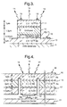
- Figures 3 and 4 show schematic diagrams of the diode structures.
- 1-x Al x Sb and Hg 1-x Cd x Te respectively, where x is the composition.
- the structure is grown epitaxially on a suitable substrate.
- the array is formed on the substrate using standard techniques, such as mesa etching or ion beam milling. These techniques are conventional to one skilled in the art.
- the device shown may be based on the InSb/ In l-x Al x Sb system and has a four layer p + - p + - ⁇ - n structure, where the p + layer 8 is of the form In 0.85 Al 0.15 Sb.
- the example is given for illustrative purposes only and the device may in fact have one of a number of compositions and combinations of doping levels.
- the structure may be grown by molecular beam epitaxy on to an InSb substrate 9, the technique of which is standard to one skilled in the art [T. Ashley et al. , Semicond. Sci. Tech. 8 S386(1993)].
- the purpose of the p + layer 10 is to provide a low resistance, low injection contact to the In 0.85 Al 0.15 Sb region 8.
- the n + region 11 is 1 ⁇ m thick and is doped with silicon (Si) to an electrical level of 2 x 10 18 cm -3 .
- the p + (10) and p + (8) regions are doped with beryllium (Be) to a level of 2 x 10 18 cm -3 and have thicknesses of 1 ⁇ m and 200 ⁇ respectively.
- the composition, x, of the In l-x Al x Sb barrier 8 is 0.15.
- the central ⁇ region 12 is 1.3 ⁇ m thick and is not deliberately doped.
- Circular diodes of 300 ⁇ m diameter are fabricated by means of mesa etching to the p + region 10.
- Sputtered chromium/gold contacts 13 are applied to the top of each mesa structure and to the p + region 10.
- the infrared radiation 14 emitted from the mesa structure is also indicated.
- the surfaces of the structure may be coated with an anti reflection coating (not shown), for example, 0.7 ⁇ m of tin oxide.
- the device is based on a Hg l-x Cd x Te system and has a three layer p + - p- n + structure.
- the structure may be grown by metal organic vapour phase epitaxy using the inter-diffused multilayer process on a GaAs substrate [S.J.C. Irvine et al ., Materials Letters 2 , 305(1984)].
- This technique is conventional to one skilled in the art.
- the ⁇ and p + layers are doped with arsenic to levels of 7 x 10 15 cm -3 and 1 x 10 17 cm -3 respectively and the n + region is doped with iodine to a level of 3 x 10 17 cm -3 .
- the diode structures are defined in a monolith of the material by etching circular trenches to produce linear arrays of the required number of elements with a common contact 18 to the p + region.
- the complete mesa device is then passivated with zinc sulphide approximately 0.3 ⁇ m thick (not shown), and metallised with chromium/gold. A typical mesa diameter would be 45 ⁇ m.
- the electrical contact 19 to the mesas may be achieved by indium bump bonding the array on to a gold lead-out pattern 20 on a sapphire carrier 21. This technique is conventional to one skilled in the art.
- the wavelength range over which the thermal imaging camera operates determines the appropriate material structure for use in the luminescent diode array.
- Diode structures based on Hg 1-x Cd x Te or In l-x Al x Sb materials emit infrared radiation in the 3-5 ⁇ m wavelength region.
- Devices based on Hg l-x Cd x Te materials may also emit in the 8-13 ⁇ m wavelength region.
- the diode structures may be formed from other narrow bandgap semiconductor materials, for example Hg l-x Zn x Te or In l-x Tl x Sb.
- Figure 6 shows the negative luminescence emission spectrum 27 for a Hg l-x Cd x Te device under reverse bias.
- a single peak 28 is seen at a wavelength of approximately 8.5 ⁇ m, with a long wavelength tail extending to beyond 10 ⁇ m.
- the figure also shows the spectral response of the device 29 when used as a detector (operating in reverse mode).
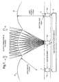
- InSb devices with the appropriate ⁇ -layer thickness for efficient negative luminescence have a reverse saturation current density in the range 15-20 A cm -2 . It is desirable to minimise this figure, whilst maintaining a high luminescence output. This can be achieved by the use of concentrators.
- lenses 30 with a radius of curvature of 120 ⁇ m are formed in degenerately doped InSb by ion beam milling.
- the technique of ion beam milling for this purpose is conventional to one skilled in the art.
- the lenses may be formed from a number of materials.
- the lenses are preferably formed from InSb and for devices based on a Hg l-x Cd x Te structure, the lenses are preferably formed from CdTe or CdZnTe.
- the diode array elements 5 are 20 ⁇ m in diameter.
- the output radiation 14 is focused into an ⁇ /2 cone (where ⁇ is the ⁇ -number) by the lenses 30.
- the radius of curvature of each lens is such that radiation emitted from each diode element 5 is not reflected back to the diode but is transmitted in a forward direction to the detector array under test.
- the lens arrangement ensures the negative luminescence efficiency is high (the negative luminescence efficiency is the proportion of infrared radiation impinging on the front surface of the device which is absorbed by the diode 5).
- the diode array is driven by means of a silicon multiplexing circuit 31, an example of which is described below.
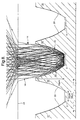
- desirable efficiencies and current densities may also be achieved by using Winston cones 32.
- the radiation 14 emitted from a 20 ⁇ m diameter diode 5 undergoes total internal reflection at the walls of the cone 33 before eventually reaching the surface of the device 34a.
- This surface 34a may be the surface of an anti reflection coating 34 applied to the array of cones.
- the shape of the cone is designed so that the emitted radiation 14 incident upon this surface 34a is at such an angle that it is transmitted rather than reflected.
- the surface area of the emitting region is kept small, therefore ensuring a low current, whilst a high negative luminescence efficiency is achieved.
- Currents equivalent to a mean current density of around 2 A cm -2 can be achieved with this arrangement.
- the cones are formed in an InSb substrate and the cone shaping is carried out by ion beam milling. Alternatively, a chemical etching may also be used to manufacture the surface in this way, the technique of which is standard to one skilled in the art.
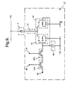
- FIG. 9 An example of the electronic circuit which may be used to supply current to the infrared light emitting diode array is shown in Figure 9.
- a positive or a negative current is applied to each diode 5 at any one instant, depending on whether the emission of positive or negative luminescence is required in a particular pixel. This is an essential feature of this circuit, or any other circuit used to drive the diode array.
- the circuit "C” is implemented at each pixel of the silicon addressing circuit.
- the circuit comprises a digital row address select line 40 and a digital column address select line 41 so that each pixel may be addressed individually.
- Two field effect transistors (FETs) 42a and 42b are associated with each pixel 5, one for row select and one for the column select.
- An external analogue voltage is supplied through another input line 43 and would require 2-level metal interconnection.
- the analogue line supplies a voltage to a complete column one at a time, even though only one pixel is addressed at any one time.
- the circuit also comprises an n-channel enhancement FET 44, a p-channel enhancement FET 45, a capacitance 46 and a resistive element 47 for current limiting purposes. In practice, this capacitance may be the gate capacitance of the FETs 44 and 45.
- the infrared light emitting diode 5 is also shown in relation to the addressing circuitry. The characteristics of the two FETs are well know to one skilled in the art and may be understood from the description in "Physics of Semiconductors Devices" (2nd Edition), by Sze (John Wiley and Sons, 1981).
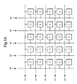
- FIG. 10 A block diagram of the row-column addressing circuit for a simple 5 x 5 array (see Figure 2) is shown in Figure 10.
- the circuit "C" (see Figure 9) is implemented at each pixel 5 of the array, with the row address lines and column address lines indicated by 47 and 48 respectively.
- the row-column addressing scheme will select the first FET switch and close it to allow charge to be placed on the capacitance 46.
- the charge on the capacitance controls the current through the diode 5 until the next reset is initiated.
- the n-channel enhancement FET 44 is ON and will pass current through the diode 5 in the polarity which produces negative luminescence.
- the n-channel enhancement mode is OFF and the p channel enhancement FET 45 is ON and will pass current through the diode 5 in the polarity which produces positive luminescence.
- Intermediate levels of charge on the diode permit the use of intermediate levels of luminescence, or "grey scales".
- the fundamental switching speed of the electroluminescent diodes is in excess of 1 MHz.
- the frame rates which may be achieved with such a system are therefore determined not by the thermal time constant of each pixel but by the frequency of the multiplexer drive circuit.
Landscapes
- Transforming Light Signals Into Electric Signals (AREA)
- Photometry And Measurement Of Optical Pulse Characteristics (AREA)
- Radiation Pyrometers (AREA)
- Testing Of Optical Devices Or Fibers (AREA)
- Light Receiving Elements (AREA)
- Led Devices (AREA)
Applications Claiming Priority (3)
| Application Number | Priority Date | Filing Date | Title |
|---|---|---|---|
| GBGB9519897.4A GB9519897D0 (en) | 1995-09-29 | 1995-09-29 | Dynamic infrared scene projector |
| GB9519897 | 1995-09-29 | ||
| PCT/GB1996/002374 WO1997013282A1 (en) | 1995-09-29 | 1996-09-26 | Dynamic infrared scene projector |
Publications (2)
| Publication Number | Publication Date |
|---|---|
| EP0852818A1 EP0852818A1 (en) | 1998-07-15 |
| EP0852818B1 true EP0852818B1 (en) | 2002-03-27 |
Family
ID=10781489
Family Applications (1)
| Application Number | Title | Priority Date | Filing Date |
|---|---|---|---|
| EP96931903A Expired - Lifetime EP0852818B1 (en) | 1995-09-29 | 1996-09-26 | Dynamic infrared scene projector |
Country Status (8)
| Country | Link |
|---|---|
| US (1) | US5949081A (enExample) |
| EP (1) | EP0852818B1 (enExample) |
| JP (1) | JP4002297B2 (enExample) |
| KR (1) | KR100418139B1 (enExample) |
| DE (1) | DE69620206T2 (enExample) |
| ES (1) | ES2171719T3 (enExample) |
| GB (2) | GB9519897D0 (enExample) |
| WO (1) | WO1997013282A1 (enExample) |
Families Citing this family (19)
| Publication number | Priority date | Publication date | Assignee | Title |
|---|---|---|---|---|
| GB9814462D0 (en) * | 1998-07-04 | 1998-09-02 | Secr Defence | Infrared light emitting diodes |
| GB2354369A (en) * | 1999-09-17 | 2001-03-21 | Secr Defence | Noise reduced semiconductor photon detectors |
| US6627907B1 (en) | 2000-09-29 | 2003-09-30 | Honeywell International Inc. | Infrared scene projector with current-mirror control electronics |
| US6485150B1 (en) | 2001-07-03 | 2002-11-26 | The United States Of America As Represented By The Secretary Of The Navy | Tunable spectral source |
| US7048384B2 (en) * | 2003-01-24 | 2006-05-23 | Honeywell International Inc. | Multiple scene projection system |
| DE10314524A1 (de) * | 2003-03-31 | 2004-10-28 | Osram Opto Semiconductors Gmbh | Scheinwerfer und Scheinwerferelement |
| DE20307956U1 (de) | 2003-05-20 | 2003-07-24 | biostep Labor- und Systemtechnik GmbH, 09387 Jahnsdorf | Imagertestgerät |
| US7473896B2 (en) * | 2005-12-21 | 2009-01-06 | Teledyne Licensing, Llc | Negative luminescence cold shield (NLCS) with microlenses to magnify the effective area of sparsely populated negative luminescence regions and method of fabrication |
| GB0607655D0 (en) * | 2006-04-18 | 2006-06-28 | Esl Defence Ltd | Apparatus for use in the testing and evaluation of infrared missile warning sensors |
| DE102006033768A1 (de) * | 2006-07-21 | 2008-01-24 | Bayerische Motoren Werke Ag | Gerät zum Testen von Infrarotkameras |
| USD631183S1 (en) | 2008-09-23 | 2011-01-18 | Lsi Industries, Inc. | Lighting fixture |
| US8215799B2 (en) | 2008-09-23 | 2012-07-10 | Lsi Industries, Inc. | Lighting apparatus with heat dissipation system |
| US8628198B2 (en) * | 2009-04-20 | 2014-01-14 | Lsi Industries, Inc. | Lighting techniques for wirelessly controlling lighting elements |
| US20100264314A1 (en) * | 2009-04-20 | 2010-10-21 | Lsi Industries, Inc. | Lighting Techniques for Wirelessly Controlling Lighting Elements |
| US8564879B1 (en) | 2010-03-26 | 2013-10-22 | The United States Of America As Represented By The Secretary Of The Navy | Multispectral infrared simulation target array |
| CN102346095B (zh) * | 2011-05-03 | 2013-07-03 | 中国兵器工业第二〇五研究所 | 中波红外二极管阵列场景生成器 |
| JP6591758B2 (ja) * | 2015-02-16 | 2019-10-16 | 旭化成エレクトロニクス株式会社 | 赤外線発光素子及び赤外線発光素子の製造方法 |
| WO2019013987A1 (en) | 2017-07-12 | 2019-01-17 | Raytheon Company | ACTIVE MULTISPECTRAL SYSTEM FOR GENERATING A CAMOUFLAGE OR OTHER RADIANT PATTERNS FROM OBJECTS IN AN INFRARED SCENE |
| US11121302B2 (en) | 2018-10-11 | 2021-09-14 | SeeQC, Inc. | System and method for superconducting multi-chip module |
Family Cites Families (2)
| Publication number | Priority date | Publication date | Assignee | Title |
|---|---|---|---|---|
| US5214292A (en) * | 1991-08-14 | 1993-05-25 | Mission Research Corporation | Dynamic infrared scene display |
| GB9420954D0 (en) * | 1994-10-18 | 1994-12-07 | Univ Keele | An infrared radiation emitting device |
-
1995
- 1995-09-29 GB GBGB9519897.4A patent/GB9519897D0/en active Pending
-
1996
- 1996-09-26 JP JP51405397A patent/JP4002297B2/ja not_active Expired - Fee Related
- 1996-09-26 US US09/043,792 patent/US5949081A/en not_active Expired - Lifetime
- 1996-09-26 KR KR10-1998-0702341A patent/KR100418139B1/ko not_active Expired - Fee Related
- 1996-09-26 ES ES96931903T patent/ES2171719T3/es not_active Expired - Lifetime
- 1996-09-26 GB GB9804051A patent/GB2319664B/en not_active Expired - Fee Related
- 1996-09-26 DE DE69620206T patent/DE69620206T2/de not_active Expired - Lifetime
- 1996-09-26 EP EP96931903A patent/EP0852818B1/en not_active Expired - Lifetime
- 1996-09-26 WO PCT/GB1996/002374 patent/WO1997013282A1/en not_active Ceased
Also Published As
| Publication number | Publication date |
|---|---|
| JPH11513489A (ja) | 1999-11-16 |
| GB9804051D0 (en) | 1998-04-22 |
| ES2171719T3 (es) | 2002-09-16 |
| WO1997013282A1 (en) | 1997-04-10 |
| GB2319664A (en) | 1998-05-27 |
| KR19990063869A (ko) | 1999-07-26 |
| KR100418139B1 (ko) | 2004-05-31 |
| EP0852818A1 (en) | 1998-07-15 |
| JP4002297B2 (ja) | 2007-10-31 |
| DE69620206D1 (de) | 2002-05-02 |
| GB9519897D0 (en) | 1995-11-29 |
| US5949081A (en) | 1999-09-07 |
| GB2319664B (en) | 1999-09-22 |
| DE69620206T2 (de) | 2002-10-24 |
Similar Documents
| Publication | Publication Date | Title |
|---|---|---|
| EP0852818B1 (en) | Dynamic infrared scene projector | |
| Baker et al. | A low-noise laser-gated imaging system for long-range target identification | |
| Rogalski | Optical detectors for focal plane arrays | |
| Brown et al. | Visible-blind UV digital camera based on a 32× 32 array of GaN/AlGaN pin photodiodes | |
| EP0429566A1 (en) | Radiation detector array using radiation sensitive bridges | |
| JPH08274376A (ja) | シリコンに格子整合したiii−v化合物半導体エミッター | |
| Bailey et al. | 256* 256 hybrid HgCdTe infrared focal plane arrays | |
| Elliott | Negative luminescence and its applications | |
| Kozlowski et al. | 640 x 480 PACE HgCdTe FPA | |
| Nash et al. | Large-area IR negative luminescent devices | |
| GB2354369A (en) | Noise reduced semiconductor photon detectors | |
| Phillips | High performance thermal imaging technology | |
| Nash et al. | Infrared negative luminescent devices and higher operating temperature detectors | |
| McEwen et al. | Albion: the UK 3rd generation high-performance thermal imaging programme | |
| Breiter et al. | High-resolution QWIP and MCT FPA modules at AIM | |
| JP2000503170A (ja) | 大規模光子放射検出器 | |
| Elliott | Sprite Detectors And Staring Arrays In Hgl_xCdxTe | |
| US20250386607A1 (en) | Colloidal Quantum Dots on a Matrix of Silicon Photomultiplier Microcells | |
| McEwen et al. | Results from the UK 3rd generation programme: Albion | |
| Nash et al. | Long wavelength infrared negative luminescent devices with strong Auger suppression | |
| Edwards et al. | A high-speed, MWIR reference source for FPA non-uniformity correction using negative luminescence | |
| Sehr et al. | Imaging and Display | |
| Nash et al. | Perspectives on dynamic infrared scene projection using positive and negative luminescence | |
| Norton et al. | Infrared detectors and detector arrays | |
| Ashley et al. | Negative luminescence |
Legal Events
| Date | Code | Title | Description |
|---|---|---|---|
| PUAI | Public reference made under article 153(3) epc to a published international application that has entered the european phase |
Free format text: ORIGINAL CODE: 0009012 |
|
| 17P | Request for examination filed |
Effective date: 19980302 |
|
| AK | Designated contracting states |
Kind code of ref document: A1 Designated state(s): BE DE ES FR IT NL SE |
|
| GRAG | Despatch of communication of intention to grant |
Free format text: ORIGINAL CODE: EPIDOS AGRA |
|
| 17Q | First examination report despatched |
Effective date: 20010412 |
|
| RAP1 | Party data changed (applicant data changed or rights of an application transferred) |
Owner name: QINETIQ LIMITED |
|
| GRAG | Despatch of communication of intention to grant |
Free format text: ORIGINAL CODE: EPIDOS AGRA |
|
| GRAH | Despatch of communication of intention to grant a patent |
Free format text: ORIGINAL CODE: EPIDOS IGRA |
|
| GRAH | Despatch of communication of intention to grant a patent |
Free format text: ORIGINAL CODE: EPIDOS IGRA |
|
| GRAA | (expected) grant |
Free format text: ORIGINAL CODE: 0009210 |
|
| AK | Designated contracting states |
Kind code of ref document: B1 Designated state(s): BE DE ES FR IT NL SE |
|
| REF | Corresponds to: |
Ref document number: 69620206 Country of ref document: DE Date of ref document: 20020502 |
|
| ET | Fr: translation filed | ||
| PGFP | Annual fee paid to national office [announced via postgrant information from national office to epo] |
Ref country code: NL Payment date: 20020815 Year of fee payment: 7 |
|
| PGFP | Annual fee paid to national office [announced via postgrant information from national office to epo] |
Ref country code: BE Payment date: 20020903 Year of fee payment: 7 |
|
| PGFP | Annual fee paid to national office [announced via postgrant information from national office to epo] |
Ref country code: ES Payment date: 20020910 Year of fee payment: 7 |
|
| REG | Reference to a national code |
Ref country code: ES Ref legal event code: FG2A Ref document number: 2171719 Country of ref document: ES Kind code of ref document: T3 |
|
| PLBE | No opposition filed within time limit |
Free format text: ORIGINAL CODE: 0009261 |
|
| STAA | Information on the status of an ep patent application or granted ep patent |
Free format text: STATUS: NO OPPOSITION FILED WITHIN TIME LIMIT |
|
| 26N | No opposition filed |
Effective date: 20021230 |
|
| PG25 | Lapsed in a contracting state [announced via postgrant information from national office to epo] |
Ref country code: ES Free format text: LAPSE BECAUSE OF NON-PAYMENT OF DUE FEES Effective date: 20030927 |
|
| PG25 | Lapsed in a contracting state [announced via postgrant information from national office to epo] |
Ref country code: BE Free format text: LAPSE BECAUSE OF NON-PAYMENT OF DUE FEES Effective date: 20030930 |
|
| BERE | Be: lapsed |
Owner name: *QINETIQ LTD Effective date: 20030930 |
|
| PG25 | Lapsed in a contracting state [announced via postgrant information from national office to epo] |
Ref country code: NL Free format text: LAPSE BECAUSE OF NON-PAYMENT OF DUE FEES Effective date: 20040401 |
|
| NLV4 | Nl: lapsed or anulled due to non-payment of the annual fee |
Effective date: 20040401 |
|
| REG | Reference to a national code |
Ref country code: ES Ref legal event code: FD2A Effective date: 20030927 |
|
| PGFP | Annual fee paid to national office [announced via postgrant information from national office to epo] |
Ref country code: SE Payment date: 20090915 Year of fee payment: 14 |
|
| PGFP | Annual fee paid to national office [announced via postgrant information from national office to epo] |
Ref country code: DE Payment date: 20090922 Year of fee payment: 14 |
|
| PGFP | Annual fee paid to national office [announced via postgrant information from national office to epo] |
Ref country code: IT Payment date: 20090926 Year of fee payment: 14 |
|
| REG | Reference to a national code |
Ref country code: SE Ref legal event code: EUG |
|
| PG25 | Lapsed in a contracting state [announced via postgrant information from national office to epo] |
Ref country code: IT Free format text: LAPSE BECAUSE OF NON-PAYMENT OF DUE FEES Effective date: 20100926 |
|
| REG | Reference to a national code |
Ref country code: DE Ref legal event code: R119 Ref document number: 69620206 Country of ref document: DE Effective date: 20110401 |
|
| PG25 | Lapsed in a contracting state [announced via postgrant information from national office to epo] |
Ref country code: DE Free format text: LAPSE BECAUSE OF NON-PAYMENT OF DUE FEES Effective date: 20110401 |
|
| PG25 | Lapsed in a contracting state [announced via postgrant information from national office to epo] |
Ref country code: SE Free format text: LAPSE BECAUSE OF NON-PAYMENT OF DUE FEES Effective date: 20100927 |
|
| PGFP | Annual fee paid to national office [announced via postgrant information from national office to epo] |
Ref country code: FR Payment date: 20121010 Year of fee payment: 17 |
|
| REG | Reference to a national code |
Ref country code: FR Ref legal event code: ST Effective date: 20140530 |
|
| PG25 | Lapsed in a contracting state [announced via postgrant information from national office to epo] |
Ref country code: FR Free format text: LAPSE BECAUSE OF NON-PAYMENT OF DUE FEES Effective date: 20130930 |