EP0848449A1 - Welded wire termination device and method - Google Patents
Welded wire termination device and method Download PDFInfo
- Publication number
- EP0848449A1 EP0848449A1 EP97121801A EP97121801A EP0848449A1 EP 0848449 A1 EP0848449 A1 EP 0848449A1 EP 97121801 A EP97121801 A EP 97121801A EP 97121801 A EP97121801 A EP 97121801A EP 0848449 A1 EP0848449 A1 EP 0848449A1
- Authority
- EP
- European Patent Office
- Prior art keywords
- conductive pad
- tubule
- wire
- welded
- termination
- Prior art date
- Legal status (The legal status is an assumption and is not a legal conclusion. Google has not performed a legal analysis and makes no representation as to the accuracy of the status listed.)
- Granted
Links
- 238000000034 method Methods 0.000 title claims description 12
- 210000005239 tubule Anatomy 0.000 claims abstract description 65
- 239000000758 substrate Substances 0.000 claims abstract description 23
- 238000003466 welding Methods 0.000 claims description 11
- 239000007787 solid Substances 0.000 abstract description 10
- OKTJSMMVPCPJKN-UHFFFAOYSA-N Carbon Chemical compound [C] OKTJSMMVPCPJKN-UHFFFAOYSA-N 0.000 description 5
- 229910002804 graphite Inorganic materials 0.000 description 5
- 239000010439 graphite Substances 0.000 description 5
- 229910000679 solder Inorganic materials 0.000 description 5
- 229920000271 Kevlar® Polymers 0.000 description 4
- 239000000463 material Substances 0.000 description 3
- RYGMFSIKBFXOCR-UHFFFAOYSA-N Copper Chemical compound [Cu] RYGMFSIKBFXOCR-UHFFFAOYSA-N 0.000 description 2
- 229910052782 aluminium Inorganic materials 0.000 description 2
- XAGFODPZIPBFFR-UHFFFAOYSA-N aluminium Chemical compound [Al] XAGFODPZIPBFFR-UHFFFAOYSA-N 0.000 description 2
- 229910052802 copper Inorganic materials 0.000 description 2
- 239000010949 copper Substances 0.000 description 2
- 206010063601 Exposure to extreme temperature Diseases 0.000 description 1
- 229910001374 Invar Inorganic materials 0.000 description 1
- ZOKXTWBITQBERF-UHFFFAOYSA-N Molybdenum Chemical compound [Mo] ZOKXTWBITQBERF-UHFFFAOYSA-N 0.000 description 1
- BQCADISMDOOEFD-UHFFFAOYSA-N Silver Chemical compound [Ag] BQCADISMDOOEFD-UHFFFAOYSA-N 0.000 description 1
- 239000000853 adhesive Substances 0.000 description 1
- 230000001070 adhesive effect Effects 0.000 description 1
- 238000003491 array Methods 0.000 description 1
- 238000005452 bending Methods 0.000 description 1
- 239000002131 composite material Substances 0.000 description 1
- 238000002788 crimping Methods 0.000 description 1
- 238000005286 illumination Methods 0.000 description 1
- 238000009413 insulation Methods 0.000 description 1
- 229910000833 kovar Inorganic materials 0.000 description 1
- 229910052751 metal Inorganic materials 0.000 description 1
- 239000002184 metal Substances 0.000 description 1
- 229910052750 molybdenum Inorganic materials 0.000 description 1
- 239000011733 molybdenum Substances 0.000 description 1
- 238000000059 patterning Methods 0.000 description 1
- 230000008439 repair process Effects 0.000 description 1
- 239000000523 sample Substances 0.000 description 1
- 229910052709 silver Inorganic materials 0.000 description 1
- 239000004332 silver Substances 0.000 description 1
- 238000005382 thermal cycling Methods 0.000 description 1
Images


Classifications
-
- H—ELECTRICITY
- H01—ELECTRIC ELEMENTS
- H01R—ELECTRICALLY-CONDUCTIVE CONNECTIONS; STRUCTURAL ASSOCIATIONS OF A PLURALITY OF MUTUALLY-INSULATED ELECTRICAL CONNECTING ELEMENTS; COUPLING DEVICES; CURRENT COLLECTORS
- H01R4/00—Electrically-conductive connections between two or more conductive members in direct contact, i.e. touching one another; Means for effecting or maintaining such contact; Electrically-conductive connections having two or more spaced connecting locations for conductors and using contact members penetrating insulation
- H01R4/02—Soldered or welded connections
- H01R4/029—Welded connections
-
- H—ELECTRICITY
- H01—ELECTRIC ELEMENTS
- H01L—SEMICONDUCTOR DEVICES NOT COVERED BY CLASS H10
- H01L31/00—Semiconductor devices sensitive to infrared radiation, light, electromagnetic radiation of shorter wavelength or corpuscular radiation and specially adapted either for the conversion of the energy of such radiation into electrical energy or for the control of electrical energy by such radiation; Processes or apparatus specially adapted for the manufacture or treatment thereof or of parts thereof; Details thereof
- H01L31/04—Semiconductor devices sensitive to infrared radiation, light, electromagnetic radiation of shorter wavelength or corpuscular radiation and specially adapted either for the conversion of the energy of such radiation into electrical energy or for the control of electrical energy by such radiation; Processes or apparatus specially adapted for the manufacture or treatment thereof or of parts thereof; Details thereof adapted as photovoltaic [PV] conversion devices
- H01L31/042—PV modules or arrays of single PV cells
- H01L31/05—Electrical interconnection means between PV cells inside the PV module, e.g. series connection of PV cells
- H01L31/0504—Electrical interconnection means between PV cells inside the PV module, e.g. series connection of PV cells specially adapted for series or parallel connection of solar cells in a module
- H01L31/0508—Electrical interconnection means between PV cells inside the PV module, e.g. series connection of PV cells specially adapted for series or parallel connection of solar cells in a module the interconnection means having a particular shape
-
- H—ELECTRICITY
- H05—ELECTRIC TECHNIQUES NOT OTHERWISE PROVIDED FOR
- H05K—PRINTED CIRCUITS; CASINGS OR CONSTRUCTIONAL DETAILS OF ELECTRIC APPARATUS; MANUFACTURE OF ASSEMBLAGES OF ELECTRICAL COMPONENTS
- H05K3/00—Apparatus or processes for manufacturing printed circuits
- H05K3/40—Forming printed elements for providing electric connections to or between printed circuits
- H05K3/4007—Surface contacts, e.g. bumps
- H05K3/4015—Surface contacts, e.g. bumps using auxiliary conductive elements, e.g. pieces of metal foil, metallic spheres
-
- H—ELECTRICITY
- H01—ELECTRIC ELEMENTS
- H01R—ELECTRICALLY-CONDUCTIVE CONNECTIONS; STRUCTURAL ASSOCIATIONS OF A PLURALITY OF MUTUALLY-INSULATED ELECTRICAL CONNECTING ELEMENTS; COUPLING DEVICES; CURRENT COLLECTORS
- H01R43/00—Apparatus or processes specially adapted for manufacturing, assembling, maintaining, or repairing of line connectors or current collectors or for joining electric conductors
- H01R43/02—Apparatus or processes specially adapted for manufacturing, assembling, maintaining, or repairing of line connectors or current collectors or for joining electric conductors for soldered or welded connections
- H01R43/0221—Laser welding
-
- Y—GENERAL TAGGING OF NEW TECHNOLOGICAL DEVELOPMENTS; GENERAL TAGGING OF CROSS-SECTIONAL TECHNOLOGIES SPANNING OVER SEVERAL SECTIONS OF THE IPC; TECHNICAL SUBJECTS COVERED BY FORMER USPC CROSS-REFERENCE ART COLLECTIONS [XRACs] AND DIGESTS
- Y02—TECHNOLOGIES OR APPLICATIONS FOR MITIGATION OR ADAPTATION AGAINST CLIMATE CHANGE
- Y02E—REDUCTION OF GREENHOUSE GAS [GHG] EMISSIONS, RELATED TO ENERGY GENERATION, TRANSMISSION OR DISTRIBUTION
- Y02E10/00—Energy generation through renewable energy sources
- Y02E10/50—Photovoltaic [PV] energy
Definitions
- This invention relates to welded wire termination and more specifically to a wire termination tab that is integrally formed with a conductive surface, and which is formable into a tubule for receiving a wire for welded termination.
- wires In many applications such as satellite solar arrays and printed circuit (PC) boards wires must be terminated to a conductive pad to interconnect circuitry and other electrical systems. Typically, the wire is soldered flat to the conductive pad. However, in high reliability thermally stressful environments solder is not a viable option. Because of the mismatch between the thermal coefficients of expansion (TCE) for the solder, the wire, the conductive pad and its underlying substrate, extended thermal cycling will fatigue the solder and may cause it to crack and eventually fail.
- TCE thermal coefficients of expansion
- a satellite for example, will thermal cycle between -180°C and +80°C for approximately 1600 cycles in a geosynchronous orbit and will thermal cycle between -80°C and +100°C for approximately 30,000 cycles in a low earth orbit.
- the wires can be terminated to a conductive pad by direct welding. Welding stranded wire to the conducive pad is difficult because the strands separate and may remain loose, thus risking a short circuit. Ensuring each strand is welded is an expensive labor intensive process. Solid wires such as diode or other component leads are difficult to weld because they are typically round and relatively thick, approximately 0.1 cm. Because they are round, the leads present only a small surface contact area with the conductive pad, which weakens the weld joint. Furthermore, the leads cannot be pressed sufficiently to reduce their thickness without sacrificing material integrity.
- a high power weld that exerts an extremely high localized pressure, for example 10,000 lbs per square inch (psi), on the underlying substrate is required.
- the weld may damage the underlying solar panel substrate which is typically formed from a thin brittle material such as graphite or Kevlar®.
- a known approach is to crimp a flat lug onto the end of the wire and then weld the flat lug onto the surface of the conductive pad.
- a crimp lug that is strong enough to mechanically hold the wire strands must be relatively thick, e.g. 0.015 to 0.025 cm.
- the crimp lug is welded to the conductive pad using a pincher weld, in which opposing weld tips are placed on the surface of the lug and underneath the conductive pad, respectively. Because the lug is so thick, a force of approximately 10,000 psi has to be exerted on the weld tips to successfully weld the crimp lug to the conductive pad.
- any repairs must be done using a parallel gap weld from the top surface.
- the extreme force required during welding can damage the thin, brittle graphite or Kevlar® substrates below the conductive pad.
- crimping the wire strands is an expensive labor intensive process, in which it is difficult to capture every strand. Stray strands can potentially cause a short. Because this approach involves two connections, pad-to-lug and lug-to-wire, the overall reliability of the wire termination is reduced. In addition, the crimped lug increases the series resistance of the connection.
- the present invention provides a welded wire termination device and method that reduces the cost and improves the reliability of the welded wire termination in thermally or mechanically stressful environments.
- the tubule is tweezer welded to form a welded termination joint between the wire and the conductive tab.
- the tubule easily captures all of the stranded wires and increases the surface area of the weld since it is welded on both sides.
- a tweezer weld exerts pressure laterally on the tubule, and thus does not exert a force on the underlying substrate that could damage the substrate. This approach creates only a single electromechanical connection from the wire to the conductive pad, which is inherently more reliable than multiple connections.
- the present invention provides a high quality welded wire termination that exhibits a high reliability in a thermally stressful environment and can withstand exposure to extreme temperatures.
- a wire termination tab is formed on a conductive pad to define a tubule for receiving a wire, either stranded or solid.
- the tubule is tweezer welded to form a welded termination joint between the wire and the conductive tab.
- the tweezer weld does not exert a force on the underlying substrate that could damage the substrate.
- the tubule easily captures all of the stranded wires and increases the surface area of the weld to a solid lead.
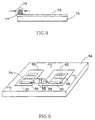
- FIG. 1 shows a termination blank 10 that includes a conductive pad 12 and a pair of wire termination tabs 14 that are integrally formed with the conductive pad 12 along an interior edge 16 and extend laterally therefrom.
- the wire termination tabs 14 are formed into tubules above the surface of the conductive pad 12 for receiving and terminating wires to the conductive pad.
- a layout designer specifies the number, size and position of the tubules on the conductive pad 12 as well as the size and shape of the pad itself.
- an end termination tab for a solar cell may include three tabs that extend out of the conductive pad for connection underneath the solar cell and include two wire termination tabs for forming tubules to interconnect adjacent end termination tabs.
- a flat sheet of metal such as silver plated copper, molybdenum, kovar or invar is punched or etched to pattern the termination blank 10 as specified.
- a die 18 is placed on the surface of the conductive pad 12 adjacent to the interior edge 16 of the wire termination tab 14 as shown in FIG. 2a
- the die preferably has an oval or circular shape so that the resulting tubule will have smoothed, and thus stronger, shape.
- the die has a diameter that is slightly larger than the diameter of the wire that will be inserted into the tubule.
- the wire termination tab 14 is formed around the die 18 to define a tubule 20 between the wire termination tab 14 and the conductive pad 12 .
- the exterior edge 22 of the wire termination tab 14 is positioned proximate to the surface of the conductive pad 12 , either just touching or slightly spaced apart from its surface.
- the die 18 is removed and the conductive pad 12 is typically mounted onto a substrate 24 such as a solar panel as shown in FIG. 2c.
- a wire having strands 28 is inserted into the tubule 20 so that all of the strands 28 are captured by the tubule.
- the tubule 20 is tweezer welded to form a welded termination joint 30 that electro-mechanically connects the strands 28 , and hence the wire, to the conductive pad.
- a tweezer weld entails placing a pair of electrodes 32 on opposites sides of the tubule 20 and forcing current through them while exerting an approximately lateral inward pressure of 15-20 lbs. The combination of heat and pressure produces the welded termination joint 30 .
- the pressure of the tweezer weld crushes the tubule inward which flattens the strands 28 and increases the surface area of the welded termination joint 30 .
- the crushed tubule 20 is preferably bent down onto the surface of the conductive pad 12 .
- a similar approach can be used for a solid wire.
- the tweezer weld does not exert a downward force on the conductive pad 12 , the underlying substrate 24 is not subjected to a localized force that could damage the substrate. Furthermore, tweezer welding the tubule produces a large and strong welded termination joint 30 that exhibits high reliability under extreme thermal conditions.
- FIGs. 3a-3b and 4a-4b depict alternate embodiments of the welded termination joint.
- the wire termination tab 14 is formed so that it defines the tubule 20 and an exterior flange 34 on the surface of the conductive pad 12 .
- the exterior flange 34 is welded to the conductive pad using a pincher weld (FIG. 3a) or a parallel gap weld (FIG. 3b).
- a pincher weld FIG. 3a
- FIG. 3b a parallel gap weld
- the exterior flange 34 can be welded before the conductive pad 12 is attached to its substrate, thus avoiding any damage to the substrate. This approach provides a stronger and more well defined tubule 20 at the cost of an additional weld.
- the wire termination tab 14 is formed so that it defines the tubule 20 and an interior flange 36 on one side of the tubule adjacent the interior edge 16 and an exterior flange 38 on the other side on the surface of the conductive pad 12 .
- the interior and exterior flanges 36 and 38 are welded to the conductive pad using a pincher weld (FIG. 4a) or a parallel gap weld (FIG. 4b).
- a solid wire 39 is inserted into the tubule and tweezer welded. This approach provides an even stronger tubule that is offset from the edge of the conductive pad at the cost of two additional welds.
- a particular application for the welded wire termination of the present invention is in interconnection of series connected solar cell strings in a satellite solar array.
- an end termination tab blank 40 is patterned with a conductive pad 42 , three solar cell termination tabs 44 that extend laterally from one side of the pad for termination to a solar cell, and three wire termination tabs 46 that extend laterally from the other side of the pad for forming respective tubules to terminate welded wires.
- the end termination tab blank 40 is formed into an end termination tab 48 having three tubules 50a , 50b , and 50c and used to clamp the soldered wires in a satellite solar array 52 as shown in FIG. 6.
- the solar array 52 includes a plurality of solar cells 54 that are connected in series to produce a desired voltage and in parallel to produce a desired current, and mounted on a solar panel substrate 56 .
- the substrate 56 provides a rigid support structure with sufficient axial and bending stiffness for carrying the solar cells through a dynamic launch environment into orbit and positioning them to receive illumination.
- the substrate 56 is suitably formed by bonding a pair of thin facesheets 60 , suitably Kevlar®, graphite or aluminum, onto opposite sides of an aluminum honeycomb core 61 .
- an insulation layer 62 is formed over the top facesheet to electrically isolate the solar cells 54 .
- the combination of the honeycomb core with the stiff facesheets provides a lightweight yet strong substrate 56 .
- the TCEs of graphite and Kevlar® are much lower than the TCEs of the end termination tab and strap. In fact graphite composite structures can have a negative TCE such that it expands when cooled and contracts when heated, which produces stress on the solar array's soldered wires.
- the solar cells 54 are connected in series to form strings 63a , 63b , ... 63n .
- Each string is terminated with an end termination tab 48 having tubules 50a , 50b , and 50c.
- the strings are connected in parallel by terminating one end of a wire 64a to via a hole 66 in the substrate to a terminal board (not shown), typically ground reference potential or the supply voltage.
- the other end of wire 64a is inserted into the opening defined by the tubule 50a on the end termination tab 48 .
- the ends of wire 64b are inserted into the tubule 50c on the first end termination tab and the tubule 50a on the second end termination tab.
- the center tubule 50b is unused in this particular application but can be used for redundant wiring or wire rework.
- the sequence is repeated for each of the n end termination tabs 48 until the last wire is terminated to the reference terminal.
- the tubules 50a and 50c are tweezer welded to form welded termination joints 68 that connect one end of the strings 63a , 63b , ... 63n in series/parallel.
- the other end of the strings 63a , 63b , ... 63n are similarly terminated to the other reference terminal to complete the series/parallel connection of the solar cells 52 .
- FIG. 7 is a plan view of a PC board 70 prior to the insertior of a stranded wire.
- a power bus 72 is integrally formed on the surface of the PC board 70 for distributing electrical signals to the circuitry on the board.
- a plurality of wire termination tabs 74 are integrally formed with the power bus 72 and extend laterally from the edge of the PC board 70 . As shown in FIG. 8, the wire termination tabs 74 are formed on a die to define a tubule 76 over the surface of the power bus 72 .
- a stranded wire 77 is inserted into the tubule 76 and tweezer welded to form a welded termination joint for communicating externals to the circuitry on the PC board 70 .
- the tubules can be used to rework terminated wires that have to be replaced. For example, if the weld joints between the leads of a diode and respective copper bus pads on a PC board become fatigued or fail, the terminated wires can be reworked by welding a pair of conductive pads formed with a tubule to the respective bus pads, inserting the leads into the tubules, and tweezer welding them to form a reliable weld termination joint. As shown in FIG. 9, a diode 78 is terminated between a pair of bus pads 80 and 82 on a PC circuit board 84 by welding its leads 86 and 88 to tubules 90 and 92 , respectively.
- the tubules are integrally formed on a pair of conductive pads 94 , 96 , which are parallel gap welded to the bus pads 80 and 82 .
- the conductive pads could be adhered directly to the PC board using a transfer adhesive.
Landscapes
- Engineering & Computer Science (AREA)
- Microelectronics & Electronic Packaging (AREA)
- Condensed Matter Physics & Semiconductors (AREA)
- Life Sciences & Earth Sciences (AREA)
- Electromagnetism (AREA)
- General Physics & Mathematics (AREA)
- Physics & Mathematics (AREA)
- Computer Hardware Design (AREA)
- Sustainable Development (AREA)
- Power Engineering (AREA)
- Manufacturing & Machinery (AREA)
- Connections Effected By Soldering, Adhesion, Or Permanent Deformation (AREA)
- Photovoltaic Devices (AREA)
Abstract
Description
Claims (10)
- A welded wire termination device, comprising a conductive pad (12; 42; 72), characterized by:a wire termination tab (14; 46; 74) formed integrally with said conductive pad to define a tubule (20; 50; 76) between the tab and the conductive pad for receiving a wire (28; 39; 64; 77) to form a welded termination joint (30; 68).
- The welded wire termination device of claim 1, characterized in that said conductive pad (12; 42; 72) has an edge (16), said termination tab (14; 46; 74) having a hinge that extends the tab away from the conductive pad (12; 42; 72) at its edge, an intermediate curvature that turns the termination tab back towards the conductive pad (12; 42; 72), and an exterior edge (22) that is proximate to said conductive pad to define the tubule (20; 50; 76; 90, 92).
- The welded wire termination device of claim 2, characterized in that the tab's exterior edge (22) forms a flange (34) that is spaced inward from the conductive pad's edge and welded to the conductive surface to define the tubule (20; 50; 76).
- The welded wire termination device of claim 1, characterized in that said conductive pad (12; 42) has an edge (16), said termination tab (14; 46; 74) having an interior flange (36) that is welded to the conductive pad (12; 42; 72) such that the tab is spaced inward from said edge and extends away from the conductive pad, an intermediate curvature that turns the termination tab back towards the conductive pad, and a exterior flange (38) that is spaced inward from the conductive pad's edge and welded to said conductive pad to define the tubule (20; 50; 76).
- A method for welded termination of a wire, characterized by the steps of:providing a termination blank (10; 40; 70) that is patterned to have a conductive pad (12; 42; 72) and at least one wire termination tab (14; 46; 74) extending laterally therefrom;forming the wire termination tab (14; 46; 74) on a die (18) to define a tubule (20; 50; 76) between the wire termination tab (14; 46; 74) and the conductive pad (12; 42; 72);inserting a wire (28; 64; 77) into the tubule; andwelding the tubule to form a welded wire termination (30; 68) between the tubule and the wire.
- The method of claim 5, characterized by the steps of:providing a substrate (24) having a conductive surface; andprior to inserting the wire (28; 64; 77) into the tubule (20; 50; 76), welding the conductive pad (12; 42; 72) to the conductive surface.
- The method of claim 5 or 6, characterized in that said wire termination tab (14; 46; 74) has an exterior edge (22), said wire termination tab (14; 46; 74) being formed on the die (18) so that the tab's exterior edge (22) is positioned proximate to a surface of the conductive pad (12; 42; 72) to define the tubule (20; 50; 76).
- The method of any of claims 5 through 7, characterized in that said wire termination tab (14; 46; 74) is formed on the die (18) so that a portion (36,38) of the termination tab (14; 46; 74) is held against a surface of the conductive pad (12; 42; 72), said portion being welded to the conductive pad (12; 42; 72) to define the tubule (20; 50; 76).
- The method of claims 5 or 8, characterized in that the tubule (20; 50; 76) is tweezer welded by:placing a pair of electrodes (32) on opposite sides of the tubule (20; 50; 76); andforcing current through the electrodes (32) while applying inward pressure on the tubule (20; 50; 76).
- The method of claim 9, characterized in that the inward pressure is applied approximately laterally to the tubule (20; 50; 76).
Applications Claiming Priority (2)
| Application Number | Priority Date | Filing Date | Title |
|---|---|---|---|
| US08/764,801 US5961737A (en) | 1996-12-12 | 1996-12-12 | Welded wire termination device and method for constructing a solar array |
| US764801 | 1996-12-12 |
Publications (2)
| Publication Number | Publication Date |
|---|---|
| EP0848449A1 true EP0848449A1 (en) | 1998-06-17 |
| EP0848449B1 EP0848449B1 (en) | 1999-08-04 |
Family
ID=25071825
Family Applications (1)
| Application Number | Title | Priority Date | Filing Date |
|---|---|---|---|
| EP97121801A Expired - Lifetime EP0848449B1 (en) | 1996-12-12 | 1997-12-11 | Welded wire termination device and method |
Country Status (3)
| Country | Link |
|---|---|
| US (2) | US5961737A (en) |
| EP (1) | EP0848449B1 (en) |
| DE (1) | DE69700382T2 (en) |
Cited By (12)
| Publication number | Priority date | Publication date | Assignee | Title |
|---|---|---|---|---|
| WO2007116088A1 (en) * | 2006-04-12 | 2007-10-18 | Pilkington Automotive Deutschland Gmbh | Glass pane having soldered electrical terminal connections |
| FR2959614A1 (en) * | 2010-04-28 | 2011-11-04 | Blue Line Holding Corp Ltd | Device for connecting wire to electric resistor of flat and flexible electric heater, has embrittlement line folding one leg part on another leg part, where opening of former part allows passage of conductor through latter part |
| EP2408260A1 (en) * | 2010-07-13 | 2012-01-18 | Saint-Gobain Glass France | Glass pane with electric connection element |
| US8277244B2 (en) | 2007-09-20 | 2012-10-02 | Saint-Gobain Glass France | Electrical connecting element and window pane provided with such an element |
| US8481857B2 (en) | 2007-12-11 | 2013-07-09 | Saint-Gobain Glass France | Windowpane having an electrical flat connecting element |
| US8816215B2 (en) | 2010-03-02 | 2014-08-26 | Saint-Gobain Glass France | Disk with an electrical connection element |
| WO2015148155A1 (en) | 2014-03-28 | 2015-10-01 | Dow Global Technologies Llc | Device and method for forming highly reliable connections in a photovoltaic components |
| US9155206B2 (en) | 2007-12-11 | 2015-10-06 | Saint-Gobain Glass France | Solder connection element |
| EP2600419A4 (en) * | 2010-07-30 | 2017-04-26 | Panasonic Intellectual Property Management Co., Ltd. | Solar cell module |
| US10305239B2 (en) | 2011-05-10 | 2019-05-28 | Saint-Gobain Glass France | Pane comprising an electrical connection element |
| US10355378B2 (en) | 2011-05-10 | 2019-07-16 | Saint-Gobain Glass France | Pane having an electrical connection element |
| US11217907B2 (en) | 2011-05-10 | 2022-01-04 | Saint-Gobain Glass France | Disk having an electric connecting element |
Families Citing this family (15)
| Publication number | Priority date | Publication date | Assignee | Title |
|---|---|---|---|---|
| US6115262A (en) | 1998-06-08 | 2000-09-05 | Ford Motor Company | Enhanced mounting pads for printed circuit boards |
| US6294725B1 (en) | 2000-03-31 | 2001-09-25 | Trw Inc. | Wireless solar cell array electrical interconnection scheme |
| US7349225B1 (en) * | 2002-10-22 | 2008-03-25 | Odyssian Technology, Llc | Multifunctional composite sandwich element with embedded electronics |
| US8153886B1 (en) * | 2003-10-20 | 2012-04-10 | Amonix, Inc. | Method of improving the efficiency of loosely packed solar cells in dense array applications |
| US20070137639A1 (en) * | 2005-12-16 | 2007-06-21 | Rhodes Richard O | Thin film solar collector |
| US8161963B2 (en) * | 2005-12-16 | 2012-04-24 | Rhodes Richard O | Thin film solar collector |
| DE102008022056B4 (en) * | 2008-05-03 | 2013-10-10 | Lumberg Connect Gmbh | Junction box, especially for solar modules |
| US8263852B2 (en) * | 2008-06-23 | 2012-09-11 | Atomic Energy Council—Institute of Nuclear Energy Research | Insulating device of concentration photovoltaic heat sink |
| US8561878B2 (en) * | 2010-09-27 | 2013-10-22 | Banyan Energy, Inc. | Linear cell stringing |
| US8231044B2 (en) | 2010-10-01 | 2012-07-31 | Orthodyne Electronics Corporation | Solar substrate ribbon bonding system |
| US8601753B2 (en) * | 2011-01-27 | 2013-12-10 | Certainteed Corporation | Electrical wiring systems for use in roofing applications |
| US8720132B2 (en) | 2011-01-27 | 2014-05-13 | Certainteed Corporation | Electrical wiring systems for use in roofing applications |
| US8863451B2 (en) | 2011-11-03 | 2014-10-21 | Certainteed Corporation | Photovoltaic roofing systems and methods for repairing them |
| DE102017131371A1 (en) | 2017-12-28 | 2019-07-04 | Te Connectivity Germany Gmbh | Mechanical connection element, electrical contact device and electrical connector |
| US11257969B2 (en) * | 2018-03-15 | 2022-02-22 | The Boeing Company | Blocking diode board for rollable solar power module |
Citations (4)
| Publication number | Priority date | Publication date | Assignee | Title |
|---|---|---|---|---|
| DE3629864A1 (en) * | 1985-09-02 | 1987-03-05 | Hitachi Ltd | Device and method for welding thin wires |
| US4943687A (en) * | 1988-01-14 | 1990-07-24 | Robert Bosch Gmbh | Current collecting unit |
| US4966565A (en) * | 1988-10-13 | 1990-10-30 | Yazaki Corporation | Crimp-style terminal and method of connecting crimp-style terminal and electric cable together |
| EP0490723A1 (en) * | 1990-12-08 | 1992-06-17 | Saint-Gobain Vitrage International | Heated laminated glass window with a cable connecting element |
Family Cites Families (8)
| Publication number | Priority date | Publication date | Assignee | Title |
|---|---|---|---|---|
| US3340096A (en) * | 1962-02-26 | 1967-09-05 | Spectrolab A Division Of Textr | Solar cell array |
| US3620847A (en) * | 1969-05-05 | 1971-11-16 | Us Air Force | Silicon solar cell array hardened to space nuclear blast radiation |
| US4034152A (en) * | 1973-06-18 | 1977-07-05 | Warner Allan S | Termination system for fusing aluminum-type lead wires |
| US4724011A (en) * | 1983-05-16 | 1988-02-09 | Atlantic Richfield Company | Solar cell interconnection by discrete conductive regions |
| US4854974A (en) * | 1987-06-29 | 1989-08-08 | Solarex Corporation | Electrical contacts for a thin-film semiconductor device |
| US5365088A (en) * | 1988-08-02 | 1994-11-15 | Santa Barbara Research Center | Thermal/mechanical buffer for HgCdTe/Si direct hybridization |
| US5057661A (en) * | 1989-10-26 | 1991-10-15 | Globe Products Inc. | Process for terminating insulated conductor wires |
| US5503684A (en) * | 1994-12-30 | 1996-04-02 | Silicon Energy Corporation | Termination system for solar panels |
-
1996
- 1996-12-12 US US08/764,801 patent/US5961737A/en not_active Expired - Lifetime
-
1997
- 1997-12-11 DE DE69700382T patent/DE69700382T2/en not_active Expired - Lifetime
- 1997-12-11 EP EP97121801A patent/EP0848449B1/en not_active Expired - Lifetime
-
1999
- 1999-03-26 US US09/277,260 patent/US6215083B1/en not_active Expired - Lifetime
Patent Citations (4)
| Publication number | Priority date | Publication date | Assignee | Title |
|---|---|---|---|---|
| DE3629864A1 (en) * | 1985-09-02 | 1987-03-05 | Hitachi Ltd | Device and method for welding thin wires |
| US4943687A (en) * | 1988-01-14 | 1990-07-24 | Robert Bosch Gmbh | Current collecting unit |
| US4966565A (en) * | 1988-10-13 | 1990-10-30 | Yazaki Corporation | Crimp-style terminal and method of connecting crimp-style terminal and electric cable together |
| EP0490723A1 (en) * | 1990-12-08 | 1992-06-17 | Saint-Gobain Vitrage International | Heated laminated glass window with a cable connecting element |
Cited By (20)
| Publication number | Priority date | Publication date | Assignee | Title |
|---|---|---|---|---|
| WO2007116088A1 (en) * | 2006-04-12 | 2007-10-18 | Pilkington Automotive Deutschland Gmbh | Glass pane having soldered electrical terminal connections |
| US8277244B2 (en) | 2007-09-20 | 2012-10-02 | Saint-Gobain Glass France | Electrical connecting element and window pane provided with such an element |
| US8485840B2 (en) | 2007-09-20 | 2013-07-16 | Saint-Gobain Glass France | Electrical connecting element and disk equipped with such an element |
| US9155206B2 (en) | 2007-12-11 | 2015-10-06 | Saint-Gobain Glass France | Solder connection element |
| US8481857B2 (en) | 2007-12-11 | 2013-07-09 | Saint-Gobain Glass France | Windowpane having an electrical flat connecting element |
| US8816215B2 (en) | 2010-03-02 | 2014-08-26 | Saint-Gobain Glass France | Disk with an electrical connection element |
| US8816214B2 (en) | 2010-03-02 | 2014-08-26 | Saint Gobain Glass France | Disk with an electrical connection element |
| FR2959614A1 (en) * | 2010-04-28 | 2011-11-04 | Blue Line Holding Corp Ltd | Device for connecting wire to electric resistor of flat and flexible electric heater, has embrittlement line folding one leg part on another leg part, where opening of former part allows passage of conductor through latter part |
| AU2011278494C1 (en) * | 2010-07-13 | 2014-11-20 | Saint-Gobain Glass France | Disc comprising an electrical connection element |
| AU2011278494B2 (en) * | 2010-07-13 | 2014-01-09 | Saint-Gobain Glass France | Disc comprising an electrical connection element |
| WO2012007303A1 (en) * | 2010-07-13 | 2012-01-19 | Saint-Gobain Glass France | Disc comprising an electrical connection element |
| EP2408260A1 (en) * | 2010-07-13 | 2012-01-18 | Saint-Gobain Glass France | Glass pane with electric connection element |
| US9385437B2 (en) | 2010-07-13 | 2016-07-05 | Saint-Gobain Glass France | Disc comprising an electrical connection element |
| EA025251B1 (en) * | 2010-07-13 | 2016-12-30 | Сэн-Гобэн Гласс Франс | Glass pane with electric connection element |
| EP2600419A4 (en) * | 2010-07-30 | 2017-04-26 | Panasonic Intellectual Property Management Co., Ltd. | Solar cell module |
| US10305239B2 (en) | 2011-05-10 | 2019-05-28 | Saint-Gobain Glass France | Pane comprising an electrical connection element |
| US10355378B2 (en) | 2011-05-10 | 2019-07-16 | Saint-Gobain Glass France | Pane having an electrical connection element |
| US11217907B2 (en) | 2011-05-10 | 2022-01-04 | Saint-Gobain Glass France | Disk having an electric connecting element |
| US11456546B2 (en) | 2011-05-10 | 2022-09-27 | Saint-Gobain Glass France | Pane having an electrical connection element |
| WO2015148155A1 (en) | 2014-03-28 | 2015-10-01 | Dow Global Technologies Llc | Device and method for forming highly reliable connections in a photovoltaic components |
Also Published As
| Publication number | Publication date |
|---|---|
| DE69700382D1 (en) | 1999-09-09 |
| US6215083B1 (en) | 2001-04-10 |
| DE69700382T2 (en) | 2000-04-06 |
| US5961737A (en) | 1999-10-05 |
| EP0848449B1 (en) | 1999-08-04 |
Similar Documents
| Publication | Publication Date | Title |
|---|---|---|
| US5961737A (en) | Welded wire termination device and method for constructing a solar array | |
| US6313396B1 (en) | Lightweight solar module and method of fabrication | |
| US6531653B1 (en) | Low cost high solar flux photovoltaic concentrator receiver | |
| US6293803B1 (en) | Zee electrical interconnect | |
| US20020151196A1 (en) | Electrical connecting element and method of producing the same | |
| JPH1079586A (en) | Heat-receiving slab structure of heat-dissipating device | |
| US5948175A (en) | Strap device clamping soldered wires for use in solar cell arrays | |
| WO1997037373A2 (en) | Method for connecting area grid arrays to printed wire board | |
| KR20000052322A (en) | Flexible circuit compression connector system and method of manufacture | |
| CA2017743C (en) | Ultra-tall indium or alloy bump array for ir detector hybrids and micro-electronics | |
| GB2107928A (en) | Solar cell assembly | |
| US9490566B2 (en) | Terminal holder | |
| US5288959A (en) | Device for electrically interconnecting opposed contact arrays | |
| US6347901B1 (en) | Solder interconnect techniques | |
| US6369331B1 (en) | Printed circuit board for semiconductor package and method of making same | |
| US7479604B1 (en) | Flexible appliance and related method for orthogonal, non-planar interconnections | |
| US6132226A (en) | Structure and method for mounting an electronic part | |
| TW200531365A (en) | Land grid array socket connector | |
| EP0792519B1 (en) | Interconnection elements for microelectronic components | |
| US11575056B1 (en) | Repairing a solar cell bonded on a flexible circuit | |
| CN216488531U (en) | Shape memory alloy wire fixing end and fixing product | |
| JPH065633B2 (en) | Connection method between wiring board and connector | |
| WO2022058311A1 (en) | Electronic module and method for connecting several conductors to a substrate | |
| JP3293348B2 (en) | Connector pin connection device and method of assembling the same | |
| JP4543650B2 (en) | Solar cell electrode structure |
Legal Events
| Date | Code | Title | Description |
|---|---|---|---|
| PUAI | Public reference made under article 153(3) epc to a published international application that has entered the european phase |
Free format text: ORIGINAL CODE: 0009012 |
|
| AK | Designated contracting states |
Kind code of ref document: A1 Designated state(s): DE FR GB IT NL |
|
| AX | Request for extension of the european patent |
Free format text: AL;LT;LV;MK;RO;SI |
|
| 17P | Request for examination filed |
Effective date: 19980729 |
|
| RAP1 | Party data changed (applicant data changed or rights of an application transferred) |
Owner name: HUGHES ELECTRONICS CORPORATION |
|
| 17Q | First examination report despatched |
Effective date: 19980922 |
|
| GRAG | Despatch of communication of intention to grant |
Free format text: ORIGINAL CODE: EPIDOS AGRA |
|
| GRAG | Despatch of communication of intention to grant |
Free format text: ORIGINAL CODE: EPIDOS AGRA |
|
| GRAH | Despatch of communication of intention to grant a patent |
Free format text: ORIGINAL CODE: EPIDOS IGRA |
|
| AKX | Designation fees paid |
Free format text: DE FR GB IT NL |
|
| RBV | Designated contracting states (corrected) |
Designated state(s): DE FR GB IT NL |
|
| GRAH | Despatch of communication of intention to grant a patent |
Free format text: ORIGINAL CODE: EPIDOS IGRA |
|
| GRAA | (expected) grant |
Free format text: ORIGINAL CODE: 0009210 |
|
| AK | Designated contracting states |
Kind code of ref document: B1 Designated state(s): DE FR GB IT NL |
|
| REF | Corresponds to: |
Ref document number: 69700382 Country of ref document: DE Date of ref document: 19990909 |
|
| ITF | It: translation for a ep patent filed | ||
| ET | Fr: translation filed | ||
| PLBE | No opposition filed within time limit |
Free format text: ORIGINAL CODE: 0009261 |
|
| STAA | Information on the status of an ep patent application or granted ep patent |
Free format text: STATUS: NO OPPOSITION FILED WITHIN TIME LIMIT |
|
| 26N | No opposition filed | ||
| REG | Reference to a national code |
Ref country code: GB Ref legal event code: IF02 |
|
| PGFP | Annual fee paid to national office [announced via postgrant information from national office to epo] |
Ref country code: NL Payment date: 20061221 Year of fee payment: 10 |
|
| NLV4 | Nl: lapsed or anulled due to non-payment of the annual fee |
Effective date: 20080701 |
|
| PG25 | Lapsed in a contracting state [announced via postgrant information from national office to epo] |
Ref country code: NL Free format text: LAPSE BECAUSE OF NON-PAYMENT OF DUE FEES Effective date: 20080701 |
|
| REG | Reference to a national code |
Ref country code: FR Ref legal event code: PLFP Year of fee payment: 19 |
|
| REG | Reference to a national code |
Ref country code: FR Ref legal event code: PLFP Year of fee payment: 20 |
|
| PG25 | Lapsed in a contracting state [announced via postgrant information from national office to epo] |
Ref country code: IT Free format text: LAPSE BECAUSE OF NON-PAYMENT OF DUE FEES Effective date: 20151211 |
|
| PGFP | Annual fee paid to national office [announced via postgrant information from national office to epo] |
Ref country code: GB Payment date: 20161228 Year of fee payment: 20 |
|
| PGFP | Annual fee paid to national office [announced via postgrant information from national office to epo] |
Ref country code: FR Payment date: 20161227 Year of fee payment: 20 |
|
| PGFP | Annual fee paid to national office [announced via postgrant information from national office to epo] |
Ref country code: DE Payment date: 20161229 Year of fee payment: 20 |
|
| PG25 | Lapsed in a contracting state [announced via postgrant information from national office to epo] |
Ref country code: IT Free format text: LAPSE BECAUSE OF NON-PAYMENT OF DUE FEES Effective date: 20151211 |
|
| PGFP | Annual fee paid to national office [announced via postgrant information from national office to epo] |
Ref country code: IT Payment date: 20161222 Year of fee payment: 20 |
|
| PGRI | Patent reinstated in contracting state [announced from national office to epo] |
Ref country code: IT Effective date: 20170710 |
|
| REG | Reference to a national code |
Ref country code: DE Ref legal event code: R071 Ref document number: 69700382 Country of ref document: DE |
|
| REG | Reference to a national code |
Ref country code: GB Ref legal event code: PE20 Expiry date: 20171210 |
|
| PG25 | Lapsed in a contracting state [announced via postgrant information from national office to epo] |
Ref country code: GB Free format text: LAPSE BECAUSE OF EXPIRATION OF PROTECTION Effective date: 20171210 |