US11575056B1 - Repairing a solar cell bonded on a flexible circuit - Google Patents
Repairing a solar cell bonded on a flexible circuit Download PDFInfo
- Publication number
- US11575056B1 US11575056B1 US17/337,890 US202117337890A US11575056B1 US 11575056 B1 US11575056 B1 US 11575056B1 US 202117337890 A US202117337890 A US 202117337890A US 11575056 B1 US11575056 B1 US 11575056B1
- Authority
- US
- United States
- Prior art keywords
- solar cell
- replacement
- interconnects
- substrate
- existing
- Prior art date
- Legal status (The legal status is an assumption and is not a legal conclusion. Google has not performed a legal analysis and makes no representation as to the accuracy of the status listed.)
- Active
Links
- 239000000758 substrate Substances 0.000 claims abstract description 67
- 239000004020 conductor Substances 0.000 claims abstract description 31
- 238000000034 method Methods 0.000 claims abstract description 29
- 239000000853 adhesive Substances 0.000 claims abstract description 12
- 230000001070 adhesive effect Effects 0.000 claims abstract description 12
- 238000005476 soldering Methods 0.000 claims abstract description 11
- 238000003466 welding Methods 0.000 claims abstract description 11
- 230000002950 deficient Effects 0.000 claims description 40
- 239000002184 metal Substances 0.000 claims description 18
- 229910052751 metal Inorganic materials 0.000 claims description 18
- 239000010949 copper Substances 0.000 description 20
- 239000011888 foil Substances 0.000 description 12
- 239000004642 Polyimide Substances 0.000 description 6
- 229920001721 polyimide Polymers 0.000 description 6
- 238000010586 diagram Methods 0.000 description 4
- 239000000463 material Substances 0.000 description 4
- 238000004519 manufacturing process Methods 0.000 description 3
- 239000010931 gold Substances 0.000 description 2
- 238000012423 maintenance Methods 0.000 description 2
- 230000004048 modification Effects 0.000 description 2
- 238000012986 modification Methods 0.000 description 2
- 229910000679 solder Inorganic materials 0.000 description 2
- RYGMFSIKBFXOCR-UHFFFAOYSA-N Copper Chemical compound [Cu] RYGMFSIKBFXOCR-UHFFFAOYSA-N 0.000 description 1
- BQCADISMDOOEFD-UHFFFAOYSA-N Silver Chemical compound [Ag] BQCADISMDOOEFD-UHFFFAOYSA-N 0.000 description 1
- 238000009825 accumulation Methods 0.000 description 1
- 229910052782 aluminium Inorganic materials 0.000 description 1
- XAGFODPZIPBFFR-UHFFFAOYSA-N aluminium Chemical compound [Al] XAGFODPZIPBFFR-UHFFFAOYSA-N 0.000 description 1
- 230000008901 benefit Effects 0.000 description 1
- 238000004140 cleaning Methods 0.000 description 1
- 239000002131 composite material Substances 0.000 description 1
- 229910052802 copper Inorganic materials 0.000 description 1
- 239000006059 cover glass Substances 0.000 description 1
- 238000013461 design Methods 0.000 description 1
- 229910003460 diamond Inorganic materials 0.000 description 1
- 239000010432 diamond Substances 0.000 description 1
- PCHJSUWPFVWCPO-UHFFFAOYSA-N gold Chemical compound [Au] PCHJSUWPFVWCPO-UHFFFAOYSA-N 0.000 description 1
- 229910052737 gold Inorganic materials 0.000 description 1
- 238000009413 insulation Methods 0.000 description 1
- 230000010354 integration Effects 0.000 description 1
- 230000013011 mating Effects 0.000 description 1
- 230000008520 organization Effects 0.000 description 1
- 238000002360 preparation method Methods 0.000 description 1
- 230000037452 priming Effects 0.000 description 1
- 230000008569 process Effects 0.000 description 1
- 238000009419 refurbishment Methods 0.000 description 1
- 230000008439 repair process Effects 0.000 description 1
- 230000004044 response Effects 0.000 description 1
- 229910052709 silver Inorganic materials 0.000 description 1
- 239000004332 silver Substances 0.000 description 1
Images


Classifications
-
- H—ELECTRICITY
- H01—ELECTRIC ELEMENTS
- H01L—SEMICONDUCTOR DEVICES NOT COVERED BY CLASS H10
- H01L31/00—Semiconductor devices sensitive to infrared radiation, light, electromagnetic radiation of shorter wavelength or corpuscular radiation and specially adapted either for the conversion of the energy of such radiation into electrical energy or for the control of electrical energy by such radiation; Processes or apparatus specially adapted for the manufacture or treatment thereof or of parts thereof; Details thereof
- H01L31/04—Semiconductor devices sensitive to infrared radiation, light, electromagnetic radiation of shorter wavelength or corpuscular radiation and specially adapted either for the conversion of the energy of such radiation into electrical energy or for the control of electrical energy by such radiation; Processes or apparatus specially adapted for the manufacture or treatment thereof or of parts thereof; Details thereof adapted as photovoltaic [PV] conversion devices
- H01L31/042—PV modules or arrays of single PV cells
- H01L31/043—Mechanically stacked PV cells
-
- H—ELECTRICITY
- H01—ELECTRIC ELEMENTS
- H01L—SEMICONDUCTOR DEVICES NOT COVERED BY CLASS H10
- H01L31/00—Semiconductor devices sensitive to infrared radiation, light, electromagnetic radiation of shorter wavelength or corpuscular radiation and specially adapted either for the conversion of the energy of such radiation into electrical energy or for the control of electrical energy by such radiation; Processes or apparatus specially adapted for the manufacture or treatment thereof or of parts thereof; Details thereof
- H01L31/04—Semiconductor devices sensitive to infrared radiation, light, electromagnetic radiation of shorter wavelength or corpuscular radiation and specially adapted either for the conversion of the energy of such radiation into electrical energy or for the control of electrical energy by such radiation; Processes or apparatus specially adapted for the manufacture or treatment thereof or of parts thereof; Details thereof adapted as photovoltaic [PV] conversion devices
- H01L31/042—PV modules or arrays of single PV cells
- H01L31/05—Electrical interconnection means between PV cells inside the PV module, e.g. series connection of PV cells
- H01L31/0504—Electrical interconnection means between PV cells inside the PV module, e.g. series connection of PV cells specially adapted for series or parallel connection of solar cells in a module
-
- H—ELECTRICITY
- H01—ELECTRIC ELEMENTS
- H01L—SEMICONDUCTOR DEVICES NOT COVERED BY CLASS H10
- H01L31/00—Semiconductor devices sensitive to infrared radiation, light, electromagnetic radiation of shorter wavelength or corpuscular radiation and specially adapted either for the conversion of the energy of such radiation into electrical energy or for the control of electrical energy by such radiation; Processes or apparatus specially adapted for the manufacture or treatment thereof or of parts thereof; Details thereof
- H01L31/18—Processes or apparatus specially adapted for the manufacture or treatment of these devices or of parts thereof
- H01L31/186—Particular post-treatment for the devices, e.g. annealing, impurity gettering, short-circuit elimination, recrystallisation
-
- Y—GENERAL TAGGING OF NEW TECHNOLOGICAL DEVELOPMENTS; GENERAL TAGGING OF CROSS-SECTIONAL TECHNOLOGIES SPANNING OVER SEVERAL SECTIONS OF THE IPC; TECHNICAL SUBJECTS COVERED BY FORMER USPC CROSS-REFERENCE ART COLLECTIONS [XRACs] AND DIGESTS
- Y02—TECHNOLOGIES OR APPLICATIONS FOR MITIGATION OR ADAPTATION AGAINST CLIMATE CHANGE
- Y02E—REDUCTION OF GREENHOUSE GAS [GHG] EMISSIONS, RELATED TO ENERGY GENERATION, TRANSMISSION OR DISTRIBUTION
- Y02E10/00—Energy generation through renewable energy sources
- Y02E10/50—Photovoltaic [PV] energy
-
- Y—GENERAL TAGGING OF NEW TECHNOLOGICAL DEVELOPMENTS; GENERAL TAGGING OF CROSS-SECTIONAL TECHNOLOGIES SPANNING OVER SEVERAL SECTIONS OF THE IPC; TECHNICAL SUBJECTS COVERED BY FORMER USPC CROSS-REFERENCE ART COLLECTIONS [XRACs] AND DIGESTS
- Y02—TECHNOLOGIES OR APPLICATIONS FOR MITIGATION OR ADAPTATION AGAINST CLIMATE CHANGE
- Y02P—CLIMATE CHANGE MITIGATION TECHNOLOGIES IN THE PRODUCTION OR PROCESSING OF GOODS
- Y02P70/00—Climate change mitigation technologies in the production process for final industrial or consumer products
- Y02P70/50—Manufacturing or production processes characterised by the final manufactured product
Definitions
- the disclosure is related generally to repairing a solar cell bonded on a flexible circuit.
- extracting and removing the existing solar cell relies on the skill of an operator in removing the existing solar cell that is damaged or defective, since connection tabs and contact pads need to be preserved, and also to minimize collateral damage. Moreover, extracting and removing the existing solar cell takes more time than is desired.
- the present disclosure describes a method of repairing an existing solar cell bonded on a substrate, by bonding a replacement solar cell on top of the existing solar cell, without removing the entire existing solar cell.
- the substrate may comprise a flexible circuit, printed circuit board, flex blanket, or panel.
- the bonding of the replacement solar cell on top of the existing solar cell uses a controlled adhesive pattern.
- Electrical connections for the existing and replacement solar cells are made using electrical conductors on, above or embedded within the substrate.
- the electrical connections may extend underneath the replacement solar cell.
- the method further comprises removing interconnects for the electrical connections for the existing solar cell, welding or soldering interconnects for the electrical connections for the replacement solar cell to the substrate, welding or soldering interconnects for the electrical connections for the replacement solar cell above the substrate, and/or welding or soldering interconnects for the electrical connections for the replacement solar cell outside a stack comprised of the replacement solar cell bonded to the existing solar cell.
- FIG. 1 illustrates one possible structure for a solar cell panel
- FIGS. 2 , 3 and 4 are cross-sectional side views of a first example where electrical connections for the solar cells are made onto a substrate;
- FIGS. 5 , 6 , 7 and 8 are cross-sectional side views of a second example where electrical connections for the solar cells are made above a substrate and panel;
- FIGS. 9 , 10 and 11 are cross-sectional side views of a third example where electrical connections for the solar cells are made above a substrate;
- FIGS. 12 , 13 and 14 illustrate examples of the disclosure made in the context of aerospace applications.
- FIG. 15 illustrates an example of the disclosure made in the form of a functional block diagram.
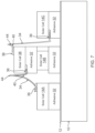
- FIG. 1 illustrates one possible structure for a solar cell panel 10 , which includes a substrate 12 , a plurality of solar cells 14 arranged in an array 16 and bonded to the substrate 12 , and electrical connections 18 between the solar cells 14 .
- the substrate 12 may be a flexible circuit, also known as a flex sheet assembly.
- the electrical connections 18 between solar cells 14 may be made using electrical conductors on, above, or embedded within the substrate 12 .
- the electrical connections 18 may comprise series connections between the solar cells 14 , or may terminate a resulting circuit so that current may be brought off of the panel 10 .
- the defective solar cell 14 may need to be replaced.
- Solar cell 14 replacement on a solar cell panel 10 currently requires mechanical removal of an existing defective solar cell 14 and bonding of a replacement solar cell 14 in its place.
- This disclosure describes a method of repairing the existing defective solar cell 14 by bonding the replacement solar cell 14 on top of the existing defective solar cell 14 with minimal removal effort of the existing defective solar cell 14 .
- surface preparation may be performed, e.g., using a diamond coated tip scriber to scribe the coverglass, as well as cleaning and priming the two mating surfaces.
- the method applies to solar cells 14 bonded to substrates 12 comprising flexible circuits, printed circuit boards or flex blankets, as well as solar cell panels 10 .
- This disclosure reduces the amount of time necessary to repair an existing defective solar cell 14 .
- prior methods of repairing solar cells 14 may damage the substrate 12 and/or solar cell panel 10 , for example, disturbing or compromising insulation underneath the existing defective solar cell 14 can result in the shorting of the solar cell 14 string to the substrate 12 with a resulting power loss, while this disclosure leaves the substrate 12 and/or solar cell panel 10 , and their components almost undisturbed. Consequently, this disclosure results in both cost savings and as well as increased product reliability.
- a key feature of this disclosure includes a method of bonding the replacement solar cell 14 on top of the existing defective solar cell 14 .
- Another feature is the bonding of the replacement solar cell 14 on top of the existing defective solar cell 14 using a controlled adhesive pattern.
- Yet another feature is that several different versions of electrical connections 18 are provided: (1) a first version is to weld and/or solder the electrical connections 18 for the replacement solar cell 14 to the substrate 12 ; (2) a second version is to weld and/or solder the electrical connections 18 outside a stack comprised of the replacement solar cell 14 bonded to the existing defective solar cell 14 ; and (3) a third version is to place the electrical connections 18 underneath the replacement solar cell 14 , so that the electrical connections 18 are essentially hidden. All of these combinations are different from the general bonding of a solar cell 14 on top of another solar cell 14 .
- FIG. 2 shows a cross-sectional side view of a first example, wherein the substrate 12 may include, inter alia, a KaptonTM or polyimide base layer 20 with multilayer electrical conductors 22 comprising one or more Copper (Cu) layers 24 A deposited on a top surface of the polyimide base layer 20 and one or more Cu layers 24 B deposited on a bottom surface of the polyimide base layer 20 , wherein a via 26 electrically connects Cu layer 24 A with Cu layer 24 B.
- Cu Copper
- the Cu layer 24 A which may be with plated with Silver (Ag) or Gold (Au) (not shown), may be patterned to form electrical conductors 22 on the surface of the substrate 12 , while the Cu layer 24 B may be patterned to form electrical conductors 22 embedded within the substrate 12 .
- the structure of the substrate 12 enables the electrical conductors 22 of the Cu layer 24 B, and thus the electrical connections 18 , to extend underneath the solar cell 14 .
- Another polyimide layer 28 may sandwich the Cu layer 24 B with the polyimide base layer 20 , resulting in a laminate structure.
- a conducting back sheet of polyimide 30 can be applied to the substrate 12 as well, which is useful in a space environment in that it will reduce the accumulation of charge.
- the solar cell 14 Shown on the right side is the solar cell 14 that is attached to the substrate 12 with an adhesive 32 . Also visible are the metal foil interconnects 34 that electrically connect to contacts 36 , such as contact pads or connection tabs, on the solar cell 14 and the Cu layer 24 A.
- FIG. 3 illustrates the example of FIG. 2 where the solar cell 14 is defective and the metal foil interconnects 34 are removed from the substrate 12 .
- the metal foil interconnects 34 may be removed from the solar cell 14 .
- This step may result in the removal of a portion of the Cu layer 24 A, and possibly other portions of the substrate 12 .
- this step may also result in the removal of a portion of the solar cell 14 , such as contacts 36 on the solar cell 14 for the interconnects 34 , and possibly other portions of the solar cell 14 .
- FIG. 4 shows a proposed method for repairing an existing solar cell 14 , based on the example of FIGS. 2 and 3 , wherein the existing solar cell 14 is defective, and a replacement solar cell 38 is bonded on top of the existing defective solar cell 14 using a controlled adhesive 32 pattern. Then, replacement interconnects 40 for the electrical connections 18 are welded or soldered to the contacts 36 of the replacement solar cell 38 , as well as the Cu layer 24 A, to electrically connect the replacement solar cell 38 to the Cu layer 24 A on the substrate 12 . Specifically, this involves welding or soldering interconnects 40 for the electrical connections 18 for the replacement solar cell 38 outside a stack comprised of the replacement solar cell 38 bonded to the existing solar cell 14 .
- an area of the Cu layer 24 A used for the electrical connection 18 may be large enough that one or more additional electrical connections 18 can be made in the area.
- the replacement interconnects 40 extending from the replacement solar cell 38 may make contact with the Cu layer 24 A in the same location as the interconnects 34 or an adjacent location that avoids the same location as the interconnects 34 , wherein the adjacent location has enough of the electrical conductor 22 for electrical current to flow around any damaged portion of the Cu layer 24 A.
- FIG. 5 shows a cross-sectional side view of a second example, wherein the metal foil interconnects 34 electrically connect the solar cells 14 A, 14 B, 14 C bonded to the substrate 12 and the panel 10 , which is shown as a rigid composite/aluminum honeycomb panel 10 .
- FIG. 6 illustrates the example of FIG. 5 , where the existing solar cell 14 B is defective and the metal foil interconnects 34 from the solar cell 14 A are removed from the existing defective solar cell 14 B, and the metal foil interconnects 34 to the solar cell 14 C are removed from the existing defective solar cell 14 B.
- This step may also result in the removal of portions of the existing defective solar cell 14 B indicated by dashed lines 42 , such as contacts 36 for the interconnects 34 , and possibly other portions of the existing defective solar cell 14 B.
- FIG. 7 shows a proposed method for repairing the existing defective solar cell 14 B, based on the example of FIGS. 5 and 6 , wherein a replacement solar cell 38 is bonded on top of the existing defective solar cell 14 B using a controlled adhesive 32 pattern or another material. Then, replacement interconnects 40 for the electrical connections 18 between the top contacts 36 of the solar cell 14 A and the bottom contacts 36 of the replacement solar cell 38 , and replacement interconnects 40 for the electrical connections 18 between the bottom contacts 36 of the solar cell 14 C and the top contacts 36 of the replacement solar cell 38 , are welded or soldered at connection points 44 outside and/or above the replacement cell 38 , and above the substrate 12 and panel 10 . Alternatively, the replacement interconnects 40 for the electrical connections 18 may be welded or soldered directly to the top and bottom contacts 36 of the solar cells 14 A, 14 C and 38 .
- FIG. 8 shows a proposed method for repairing the existing defective solar cell 14 B, based on the example of FIGS. 5 , 6 and 7 , wherein a replacement solar cell 38 is bonded on top of the existing defective solar cell 14 B using a controlled adhesive 32 pattern or another material. Then, replacement interconnects 40 for the electrical connections 18 between the top contacts 36 of the solar cell 14 A and the bottom contacts 36 of the replacement solar cell 38 , and replacement interconnects 40 for the electrical connections 18 between the bottom contacts 36 of the solar cell 14 C and the top contacts 36 of the replacement solar cell 38 , are welded or soldered at connection points 44 under the replacement solar cell 38 , and above the substrate 12 and panel 10 . Making the connection points 44 above the replacement cell 38 , as shown in FIG.
- the replacement interconnects 40 for the electrical connections 18 may be welded or soldered directly to the contacts 36 of solar cells 14 A, 14 C and 38 .
- FIG. 9 shows a cross-sectional side view of a third example, similar to the first and second examples, except that one of the metal foil interconnects 34 electrically connects two solar cells 14 A, 14 B above the substrate 12 without contacting the Cu layer 24 A, while others of the metal foil interconnects electrically connect the two solar cells 14 A, 14 B on the substrate 12 by contacting the Cu layers 24 A.
- FIG. 10 illustrates the example of FIG. 9 , where the existing solar cell 14 B is defective and the metal foil interconnects 34 are removed from the existing defective solar cell 14 B.
- This step may also result in the removal of a portion of the existing defective solar cell 14 B, such as contacts 36 for the interconnects 34 and possibly other portions of the existing defective solar cell 14 B.
- the metal foil interconnects 34 could be removed from the solar cell 14 A, which may also result in the removal of a portion of the solar cell 14 A, such as contacts 36 for the interconnects 34 and possibly other portions of the solar cell 14 A.
- FIG. 11 shows a proposed method for repairing the existing defective solar cell 14 B, based on the example of FIGS. 9 and 10 , wherein a replacement solar cell 38 is bonded on top of the existing defective solar cell 14 B using a controlled adhesive 32 pattern or another material. Then, replacement interconnects 40 for the electrical connections 18 are welded or soldered to the top contacts 36 of the replacement solar cell 38 , as well as the top contacts 36 of the solar cell 14 A, above the substrate 12 . The replacement interconnects 40 for the electrical connections 18 are also welded or soldered to the bottom contacts 36 of the replacement solar cell 38 to electrically connect the replacement solar cell 38 to the Cu layer 24 A. Alternatively, the replacement interconnects 40 may be welded or soldered to the metal foil interconnects 34 removed from the existing defective solar cell 14 B, where the metal foil interconnect 34 is still attached to the solar cell 14 A.
- Examples of the disclosure may be described in the context of a method 40 of fabricating a solar cell 14 , solar cell panel 10 and/or satellite, comprising steps 42 - 54 and 56 - 62 , as shown in FIGS. 12 and 13 , respectively, wherein the resulting satellite 64 having a solar cell panel 10 comprised of solar cells 14 are shown in FIG. 14 .
- exemplary method 40 may include specification and design 42 of the solar cell 14 , solar cell panel 10 and/or satellite 64 , and material procurement 44 for same.
- component and subassembly manufacturing 46 and system integration 48 of the solar cell 14 , solar cell panel 10 and/or satellite 64 takes place, which include fabricating the solar cell 14 , solar cell panel 10 and/or satellite 64 .
- the solar cell 14 , solar cell panel 10 and/or satellite 64 may go through certification and delivery 50 in order to be placed in service 52 .
- the solar cell 14 , solar cell panel 10 and/or satellite 64 may also be scheduled for maintenance and service 54 (which includes modification, reconfiguration, refurbishment, and so on), before being launched.
- the maintenance or service step 54 may include repairing 56 an existing solar cell 14 bonded on a substrate 12 , wherein the existing solar cell 14 is defective, by bonding 58 a replacement solar cell 38 on top of the existing solar cell 14 , without removing the existing solar cell 14 .
- the bonding 58 of the replacement solar cell 38 on top of the existing solar cell 14 uses a controlled adhesive 32 pattern.
- electrical connections 18 for the existing solar cell 14 and the replacement solar cell 38 are made using electrical conductors 22 on, above or embedded within the substrate 12 .
- the electrical conductors 22 extend underneath the replacement solar cell 38 .
- the repairing 56 of the existing solar cell 14 may further comprise removing 60 interconnects 34 for the electrical connections 18 for the existing solar cell 14 .
- the repairing 56 of the existing solar cell 14 may further comprise welding or soldering 62 replacement interconnects 40 for the electrical connections 18 for the replacement solar cell 38 .
- replacement interconnects 40 for the electrical connections 18 are welded or soldered to the substrate 12 , such as the Cu layer 24 A on the substrate 12 .
- replacement interconnects 40 for the electrical connections 18 are welded or soldered above the substrate 12 .
- the replacement interconnects 40 are welded or soldered outside a stack comprised of the replacement solar cell 38 bonded to the existing solar cell 14 .
- a system integrator may include without limitation any number of solar cell, solar cell panel, satellite or spacecraft manufacturers and major-system subcontractors;
- a third party may include without limitation any number of venders, subcontractors, and suppliers; and
- an operator may be a satellite company, military entity, service organization, and so on.
- a satellite 64 fabricated by exemplary method 40 may include systems 66 , a body 68 , solar cell panels 10 comprised of solar cells 14 , 38 , and one or more antennae 70 .
- the systems 66 included with the satellite 64 include, but are not limited to, one or more of a propulsion system 72 , an electrical system 74 , a communications system 76 , and a power system 78 . Any number of other systems 66 also may be included.
- FIG. 15 is an illustration of a solar cell panel 10 in the form of a functional block diagram.
- the solar cell panel 10 is comprised of a substrate 12 and one or more solar cells 14 , 38 arranged in an array 16 and bonded on the substrate 12 , wherein the substrate 12 comprises a flexible circuit, printed circuit board, or flex blanket.
- Each of the solar cells 14 , 38 absorbs light 82 from a light source 84 and generates an electrical output 86 in response thereto.
- This functional block diagram describes a method of repairing an existing solar cell 14 bonded on the substrate 12 , wherein the existing solar cell 14 is defective, by bonding a replacement solar cell 38 on top of the existing solar cell 14 , without removing the existing solar cell 14 , wherein the bonding of the replacement solar cell 38 on top of the existing solar cell 14 uses a controlled adhesive 32 pattern.
- Electrical connections 18 for the existing and replacement solar cells 14 are made using electrical conductors 22 on, above or embedded within the substrate 12 .
- the method includes removing interconnects 34 for the electrical connections 18 for the existing solar cell 14 , and welding or soldering replacement interconnects 40 for the electrical connections 18 for the replacement solar cell 38 to the substrate 12 or above the substrate 12 . This may include welding or soldering replacement interconnects 40 for the electrical connections 18 for the replacement solar cell 38 outside a stack comprised of the replacement solar cell 38 bonded to the existing solar cell 14 .
Abstract
A method of repairing a solar cell bonded on a substrate, by bonding a replacement solar cell on top of an existing solar cell, without removing the existing solar cell. The substrate may comprise a flexible circuit, printed circuit board, flex blanket, or solar cell panel. The bonding of the replacement solar cell on top of the existing solar cell uses a controlled adhesive pattern. Electrical connections for the existing solar cell and the replacement solar cell are made using electrical conductors on, above or embedded within the substrate. The electrical connections may extend underneath the replacement solar cell. The method further comprises removing interconnects for the electrical connections for the existing solar cell, and then welding or soldering interconnects for the electrical connections for the replacement solar cell.
Description
This application claims the benefit under 35 U.S.C. Section 119(e) of the following commonly-assigned application:
U.S. Provisional Application Ser. No. 63/052,278, filed on Jul. 15, 2020, by Phil Luc, entitled “REPAIRING A SOLAR CELL BONDED ON A FLEXIBLE CIRCUIT,”;
which application is incorporated by reference herein.
The disclosure is related generally to repairing a solar cell bonded on a flexible circuit.
Currently, when an existing solar cell is damaged or defective, the entire cell is typically removed from a substrate or housing upon which the existing solar cell is situated. A replacement solar cell is then situated on the substrate or housing in place of the existing solar cell and electrically interconnected to other solar cells in an array.
However, extracting and removing the existing solar cell relies on the skill of an operator in removing the existing solar cell that is damaged or defective, since connection tabs and contact pads need to be preserved, and also to minimize collateral damage. Moreover, extracting and removing the existing solar cell takes more time than is desired.
Thus, there is a need for improved methods for repairing a solar cell bonded on a flexible circuit.
To overcome the limitations described above, and to overcome other limitations that will become apparent upon reading and understanding the present specification, the present disclosure describes a method of repairing an existing solar cell bonded on a substrate, by bonding a replacement solar cell on top of the existing solar cell, without removing the entire existing solar cell. The substrate may comprise a flexible circuit, printed circuit board, flex blanket, or panel. The bonding of the replacement solar cell on top of the existing solar cell uses a controlled adhesive pattern.
Electrical connections for the existing and replacement solar cells are made using electrical conductors on, above or embedded within the substrate. The electrical connections may extend underneath the replacement solar cell.
The method further comprises removing interconnects for the electrical connections for the existing solar cell, welding or soldering interconnects for the electrical connections for the replacement solar cell to the substrate, welding or soldering interconnects for the electrical connections for the replacement solar cell above the substrate, and/or welding or soldering interconnects for the electrical connections for the replacement solar cell outside a stack comprised of the replacement solar cell bonded to the existing solar cell.
Referring now to the drawings in which like reference numbers represent corresponding parts throughout:
In the following description, reference is made to the accompanying drawings which form a part hereof, and in which is shown by way of illustration a specific example in which the disclosure may be practiced. It is to be understood that other examples may be utilized and structural changes may be made without departing from the scope of the present disclosure.
Overview
If at least one of the solar cells 14 is a defective solar cell 14, or if there is a problem with its electrical connections 18, after the defective solar cell 14 has been bonded on the substrate 12 and mounted on the solar cell panel 10, the defective solar cell 14 may need to be replaced. Solar cell 14 replacement on a solar cell panel 10 currently requires mechanical removal of an existing defective solar cell 14 and bonding of a replacement solar cell 14 in its place.
This disclosure describes a method of repairing the existing defective solar cell 14 by bonding the replacement solar cell 14 on top of the existing defective solar cell 14 with minimal removal effort of the existing defective solar cell 14. For example, surface preparation may be performed, e.g., using a diamond coated tip scriber to scribe the coverglass, as well as cleaning and priming the two mating surfaces. Moreover, the method applies to solar cells 14 bonded to substrates 12 comprising flexible circuits, printed circuit boards or flex blankets, as well as solar cell panels 10.
This disclosure reduces the amount of time necessary to repair an existing defective solar cell 14. Moreover, prior methods of repairing solar cells 14 may damage the substrate 12 and/or solar cell panel 10, for example, disturbing or compromising insulation underneath the existing defective solar cell 14 can result in the shorting of the solar cell 14 string to the substrate 12 with a resulting power loss, while this disclosure leaves the substrate 12 and/or solar cell panel 10, and their components almost undisturbed. Consequently, this disclosure results in both cost savings and as well as increased product reliability.
Thus, a key feature of this disclosure includes a method of bonding the replacement solar cell 14 on top of the existing defective solar cell 14. Another feature is the bonding of the replacement solar cell 14 on top of the existing defective solar cell 14 using a controlled adhesive pattern. Yet another feature is that several different versions of electrical connections 18 are provided: (1) a first version is to weld and/or solder the electrical connections 18 for the replacement solar cell 14 to the substrate 12; (2) a second version is to weld and/or solder the electrical connections 18 outside a stack comprised of the replacement solar cell 14 bonded to the existing defective solar cell 14; and (3) a third version is to place the electrical connections 18 underneath the replacement solar cell 14, so that the electrical connections 18 are essentially hidden. All of these combinations are different from the general bonding of a solar cell 14 on top of another solar cell 14.
The Cu layer 24A, which may be with plated with Silver (Ag) or Gold (Au) (not shown), may be patterned to form electrical conductors 22 on the surface of the substrate 12, while the Cu layer 24B may be patterned to form electrical conductors 22 embedded within the substrate 12. The structure of the substrate 12 enables the electrical conductors 22 of the Cu layer 24B, and thus the electrical connections 18, to extend underneath the solar cell 14.
Another polyimide layer 28 may sandwich the Cu layer 24B with the polyimide base layer 20, resulting in a laminate structure. A conducting back sheet of polyimide 30 can be applied to the substrate 12 as well, which is useful in a space environment in that it will reduce the accumulation of charge.
Shown on the right side is the solar cell 14 that is attached to the substrate 12 with an adhesive 32. Also visible are the metal foil interconnects 34 that electrically connect to contacts 36, such as contact pads or connection tabs, on the solar cell 14 and the Cu layer 24A.
Note that an area of the Cu layer 24A used for the electrical connection 18 may be large enough that one or more additional electrical connections 18 can be made in the area. For example, the replacement interconnects 40 extending from the replacement solar cell 38 may make contact with the Cu layer 24A in the same location as the interconnects 34 or an adjacent location that avoids the same location as the interconnects 34, wherein the adjacent location has enough of the electrical conductor 22 for electrical current to flow around any damaged portion of the Cu layer 24A.
Aerospace Applications
Examples of the disclosure may be described in the context of a method 40 of fabricating a solar cell 14, solar cell panel 10 and/or satellite, comprising steps 42-54 and 56-62, as shown in FIGS. 12 and 13 , respectively, wherein the resulting satellite 64 having a solar cell panel 10 comprised of solar cells 14 are shown in FIG. 14 .
As illustrated in FIG. 12 , during pre-production, exemplary method 40 may include specification and design 42 of the solar cell 14, solar cell panel 10 and/or satellite 64, and material procurement 44 for same. During production, component and subassembly manufacturing 46 and system integration 48 of the solar cell 14, solar cell panel 10 and/or satellite 64 takes place, which include fabricating the solar cell 14, solar cell panel 10 and/or satellite 64. Thereafter, the solar cell 14, solar cell panel 10 and/or satellite 64 may go through certification and delivery 50 in order to be placed in service 52. The solar cell 14, solar cell panel 10 and/or satellite 64 may also be scheduled for maintenance and service 54 (which includes modification, reconfiguration, refurbishment, and so on), before being launched.
As illustrated in FIG. 13 , the maintenance or service step 54 may include repairing 56 an existing solar cell 14 bonded on a substrate 12, wherein the existing solar cell 14 is defective, by bonding 58 a replacement solar cell 38 on top of the existing solar cell 14, without removing the existing solar cell 14. In one example, the bonding 58 of the replacement solar cell 38 on top of the existing solar cell 14 uses a controlled adhesive 32 pattern.
Moreover, electrical connections 18 for the existing solar cell 14 and the replacement solar cell 38 are made using electrical conductors 22 on, above or embedded within the substrate 12. In one example, the electrical conductors 22 extend underneath the replacement solar cell 38.
The repairing 56 of the existing solar cell 14 may further comprise removing 60 interconnects 34 for the electrical connections 18 for the existing solar cell 14.
The repairing 56 of the existing solar cell 14 may further comprise welding or soldering 62 replacement interconnects 40 for the electrical connections 18 for the replacement solar cell 38. In one example, replacement interconnects 40 for the electrical connections 18 are welded or soldered to the substrate 12, such as the Cu layer 24A on the substrate 12. In another example, replacement interconnects 40 for the electrical connections 18 are welded or soldered above the substrate 12. In yet another example, the replacement interconnects 40 are welded or soldered outside a stack comprised of the replacement solar cell 38 bonded to the existing solar cell 14.
Each of the processes of method 40 may be performed or carried out by a system integrator, a third party, and/or an operator (e.g., a customer). For the purposes of this description, a system integrator may include without limitation any number of solar cell, solar cell panel, satellite or spacecraft manufacturers and major-system subcontractors; a third party may include without limitation any number of venders, subcontractors, and suppliers; and an operator may be a satellite company, military entity, service organization, and so on.
As shown in FIG. 14 , a satellite 64 fabricated by exemplary method 40 may include systems 66, a body 68, solar cell panels 10 comprised of solar cells 14, 38, and one or more antennae 70. Examples of the systems 66 included with the satellite 64 include, but are not limited to, one or more of a propulsion system 72, an electrical system 74, a communications system 76, and a power system 78. Any number of other systems 66 also may be included.
Functional Block Diagram
This functional block diagram describes a method of repairing an existing solar cell 14 bonded on the substrate 12, wherein the existing solar cell 14 is defective, by bonding a replacement solar cell 38 on top of the existing solar cell 14, without removing the existing solar cell 14, wherein the bonding of the replacement solar cell 38 on top of the existing solar cell 14 uses a controlled adhesive 32 pattern. Electrical connections 18 for the existing and replacement solar cells 14 are made using electrical conductors 22 on, above or embedded within the substrate 12. The method includes removing interconnects 34 for the electrical connections 18 for the existing solar cell 14, and welding or soldering replacement interconnects 40 for the electrical connections 18 for the replacement solar cell 38 to the substrate 12 or above the substrate 12. This may include welding or soldering replacement interconnects 40 for the electrical connections 18 for the replacement solar cell 38 outside a stack comprised of the replacement solar cell 38 bonded to the existing solar cell 14.
Conclusion
The description of the examples set forth above has been presented for purposes of illustration and description, and is not intended to be exhaustive or limited to the examples described. Many alternatives, modifications and variations may be used in place of the specific elements described above.
Claims (20)
1. A method, comprising:
repairing an existing solar cell bonded on a substrate, wherein the existing solar cell is defective, by bonding a replacement solar cell on top of the existing solar cell, without removing the existing solar cell;
wherein the substrate includes at least a base layer, a first metal layer patterned to form first electrical conductors deposited on a first surface of the base layer, and a second metal layer patterned to form second electrical conductors deposited on a second surface of the base layer, wherein the second surface is opposite the first surface, and the first electrical conductors are electrically connected to the second electrical conductors;
wherein interconnects electrically connect the existing solar cell to the first electrical conductors deposited on the first surface of the base layer; and
replacement interconnects electrically connect the replacement solar cell to the first electrical conductors deposited on the first surface of the base layer, in a same location as the interconnects, or in an adjacent location that avoids the same location as the interconnects.
2. The method of claim 1 , wherein the bonding of the replacement solar cell on top of the existing solar cell uses a controlled adhesive pattern.
3. The method of claim 1 , wherein the electrical connections for the replacement solar cell are made using the replacement interconnects positioned above the substrate.
4. The method of claim 1 , wherein the second electrical conductors extend underneath the replacement solar cell.
5. The method of claim 1 , further comprising removing the interconnects for the electrical connections for the existing solar cell.
6. The method of claim 1 , further comprising welding or soldering the replacement interconnects for the electrical connections for the replacement solar cell to the substrate.
7. The method of claim 1 , further comprising welding or soldering the replacement interconnects for the electrical connections for the replacement solar cell above the substrate.
8. The method of claim 1 , further comprising welding or soldering the replacement interconnects for the electrical connections for the replacement solar cell outside a stack comprised of the replacement solar cell bonded to the existing solar cell.
9. The method of claim 1 , wherein the substrate comprises a flexible circuit, printed circuit board, flex blanket, or solar cell panel.
10. A structure, comprising:
a substrate for solar cells;
at least one existing solar cell bonded on the substrate, wherein the existing solar cell is defective; and
at least one replacement solar cell bonded on top of the existing solar cell, without removing the existing solar cell;
wherein the substrate includes at least a base layer, a first metal layer patterned to form first electrical conductors deposited on a first surface of the base layer, and a second metal layer patterned to form second electrical conductors deposited on a second surface of the base layer, wherein the second surface is opposite the first surface, and the first electrical conductors are electrically connected to the second electrical conductors;
wherein interconnects electrically connect the existing solar cell to the first electrical conductors deposited on the first surface of the base layer; and
replacement interconnects electrically connect the replacement solar cell to the first electrical conductors deposited on the first surface of the base layer, in a same location as the interconnects, or in an adjacent location that avoids the same location as the interconnects.
11. The structure of claim 10 , wherein the replacement solar cell is bonded on top of the existing solar cell using a controlled adhesive pattern.
12. The structure of claim 10 , wherein the electrical connections for the replacement solar cell are made using the replacement interconnects positioned above the substrate.
13. The structure of claim 10 , wherein the second electrical conductors extend underneath the replacement solar cell.
14. The structure of claim 10 , wherein the interconnects for the electrical connections for the existing solar cell are removed.
15. The structure of claim 10 , wherein the replacement interconnects for the electrical connections for the replacement solar cell are welded or soldered to the substrate.
16. The structure of claim 10 , wherein the replacement interconnects for the electrical connections for the replacement solar cell are welded or soldered above the substrate.
17. The structure of claim 10 , wherein the replacement interconnects for the electrical connections for the replacement solar cell are welded or soldered outside a stack comprised of the replacement solar cell bonded to the existing solar cell.
18. The structure of claim 12 , wherein the substrate comprises a flexible circuit, printed circuit board, flex blanket, or solar cell panel.
19. A solar cell panel, comprising:
a substrate;
one or more solar cells arranged in an array and bonded to the substrate, wherein at least one of the solar cells is a defective solar cell; and
at least one replacement solar cell bonded on top of the defective solar cell, without removing the defective solar cell;
wherein the substrate includes at least a base layer, a first metal layer patterned to form first electrical conductors deposited on a first surface of the base layer, and a second metal layer patterned to form second electrical conductors deposited on a second surface of the base layer, wherein the second surface is opposite the first surface, and the first electrical conductors are electrically connected to the second electrical conductors;
wherein interconnects electrically connect the existing solar cell to the first electrical conductors deposited on the first surface of the base layer; and
replacement interconnects electrically connect the replacement solar cell to the first electrical conductors deposited on the first surface of the base layer, in a same location as the interconnects, or in an adjacent location that avoids the same location as the interconnects.
20. The solar cell panel of claim 19 , wherein the electrical connections for the replacement solar cell are made using the replacement interconnects positioned above the substrate.
Priority Applications (4)
| Application Number | Priority Date | Filing Date | Title |
|---|---|---|---|
| US17/337,890 US11575056B1 (en) | 2020-07-15 | 2021-06-03 | Repairing a solar cell bonded on a flexible circuit |
| CA3123147A CA3123147A1 (en) | 2020-07-15 | 2021-06-23 | Repairing a solar cell bonded on a flexible circuit |
| EP21181959.4A EP3940797A1 (en) | 2020-07-15 | 2021-06-28 | Repairing a solar cell bonded on a flexible circuit |
| JP2021116063A JP2022019636A (en) | 2020-07-15 | 2021-07-14 | Repairing solar cell bonded onto flexible circuit |
Applications Claiming Priority (2)
| Application Number | Priority Date | Filing Date | Title |
|---|---|---|---|
| US202063052278P | 2020-07-15 | 2020-07-15 | |
| US17/337,890 US11575056B1 (en) | 2020-07-15 | 2021-06-03 | Repairing a solar cell bonded on a flexible circuit |
Publications (1)
| Publication Number | Publication Date |
|---|---|
| US11575056B1 true US11575056B1 (en) | 2023-02-07 |
Family
ID=76695521
Family Applications (1)
| Application Number | Title | Priority Date | Filing Date |
|---|---|---|---|
| US17/337,890 Active US11575056B1 (en) | 2020-07-15 | 2021-06-03 | Repairing a solar cell bonded on a flexible circuit |
Country Status (4)
| Country | Link |
|---|---|
| US (1) | US11575056B1 (en) |
| EP (1) | EP3940797A1 (en) |
| JP (1) | JP2022019636A (en) |
| CA (1) | CA3123147A1 (en) |
Citations (5)
| Publication number | Priority date | Publication date | Assignee | Title |
|---|---|---|---|---|
| US5118361A (en) * | 1990-05-21 | 1992-06-02 | The Boeing Company | Terrestrial concentrator solar cell module |
| DE20217067U1 (en) | 2002-11-04 | 2003-01-09 | Astrium Gmbh | Repair for solar panel system used replacement bonded to defective panel |
| US6809250B2 (en) | 2001-08-10 | 2004-10-26 | Astrium Gmbh | Repaired solar panel and method of preparing same |
| US20100084003A1 (en) | 2008-10-06 | 2010-04-08 | Chien-An Chen | Solar cell module |
| US20100240153A1 (en) * | 2009-03-23 | 2010-09-23 | Sanyo Electric Co., Ltd. | Manufacture method for photovoltaic module |
-
2021
- 2021-06-03 US US17/337,890 patent/US11575056B1/en active Active
- 2021-06-23 CA CA3123147A patent/CA3123147A1/en active Pending
- 2021-06-28 EP EP21181959.4A patent/EP3940797A1/en not_active Withdrawn
- 2021-07-14 JP JP2021116063A patent/JP2022019636A/en active Pending
Patent Citations (6)
| Publication number | Priority date | Publication date | Assignee | Title |
|---|---|---|---|---|
| US5118361A (en) * | 1990-05-21 | 1992-06-02 | The Boeing Company | Terrestrial concentrator solar cell module |
| US6809250B2 (en) | 2001-08-10 | 2004-10-26 | Astrium Gmbh | Repaired solar panel and method of preparing same |
| DE20217067U1 (en) | 2002-11-04 | 2003-01-09 | Astrium Gmbh | Repair for solar panel system used replacement bonded to defective panel |
| US20100084003A1 (en) | 2008-10-06 | 2010-04-08 | Chien-An Chen | Solar cell module |
| US20100240153A1 (en) * | 2009-03-23 | 2010-09-23 | Sanyo Electric Co., Ltd. | Manufacture method for photovoltaic module |
| US7998760B2 (en) * | 2009-03-23 | 2011-08-16 | Sanyo Electric Co., Ltd. | Manufacture method for photovoltaic module including inspection and repair |
Non-Patent Citations (1)
| Title |
|---|
| Extended European Search Report dated Nov. 18, 2021 for European Patent Application No. 21181959.4. |
Also Published As
| Publication number | Publication date |
|---|---|
| EP3940797A1 (en) | 2022-01-19 |
| CA3123147A1 (en) | 2022-01-15 |
| JP2022019636A (en) | 2022-01-27 |
Similar Documents
| Publication | Publication Date | Title |
|---|---|---|
| US5276955A (en) | Multilayer interconnect system for an area array interconnection using solid state diffusion | |
| EP0469308B1 (en) | Multilayered circuit board assembly and method of making same | |
| EP0526133B1 (en) | Polyimide multilayer wiring substrate and method for manufacturing the same | |
| US3973996A (en) | Diffusion welded solar cell array | |
| EP0914757B1 (en) | Z-axis interconnect method and circuit | |
| US5401913A (en) | Electrical interconnections between adjacent circuit board layers of a multi-layer circuit board | |
| US5534666A (en) | Multi-layer wiring board having a base block and a stacking block connected by an adhesive layer | |
| US20180076348A1 (en) | Rework and repair of components in a solar cell array | |
| WO1999004461A1 (en) | Interposers for land grid arrays | |
| US7385144B2 (en) | Method and apparatus for electrically connecting printed circuit boards or other panels | |
| JPH05243736A (en) | Manufacture of printed circuit board | |
| EP3297033A1 (en) | Rework and repair of components in a solar cell array | |
| US6090633A (en) | Multiple-plane pair thin-film structure and process of manufacture | |
| EP4235810A2 (en) | Rework and repair of components in a solar cell array | |
| CN101996981A (en) | Module comprising semiconductor devices and module manufacturing method | |
| US20190305723A1 (en) | Wiring for a rigid panel solar array | |
| JP2001332828A (en) | Double-sided circuit board and multilayer wiring board using the same | |
| JPH08148828A (en) | Thin film multilayered circuit board and its manufacture | |
| US11575056B1 (en) | Repairing a solar cell bonded on a flexible circuit | |
| JP3177064B2 (en) | Interconnectors and wiring boards | |
| JPH1131877A (en) | Method for testing printed wiring board and electric parts | |
| JPH1131884A (en) | Multilayered printed circuit board and electronic device | |
| US20230097056A1 (en) | Lightweight flexible solar array | |
| JP3449997B2 (en) | Semiconductor device test method and test board | |
| EP0543331A2 (en) | Polyimide multilayer interconnection board and method of making the same |
Legal Events
| Date | Code | Title | Description |
|---|---|---|---|
| FEPP | Fee payment procedure |
Free format text: ENTITY STATUS SET TO UNDISCOUNTED (ORIGINAL EVENT CODE: BIG.); ENTITY STATUS OF PATENT OWNER: LARGE ENTITY |
|
| STCF | Information on status: patent grant |
Free format text: PATENTED CASE |