EP0843352A1 - Method for removing a semiconductor chip bonded to a wire-bonded multichip module - Google Patents
Method for removing a semiconductor chip bonded to a wire-bonded multichip module Download PDFInfo
- Publication number
- EP0843352A1 EP0843352A1 EP96480106A EP96480106A EP0843352A1 EP 0843352 A1 EP0843352 A1 EP 0843352A1 EP 96480106 A EP96480106 A EP 96480106A EP 96480106 A EP96480106 A EP 96480106A EP 0843352 A1 EP0843352 A1 EP 0843352A1
- Authority
- EP
- European Patent Office
- Prior art keywords
- chip
- substrate
- stud
- glue
- temperature
- Prior art date
- Legal status (The legal status is an assumption and is not a legal conclusion. Google has not performed a legal analysis and makes no representation as to the accuracy of the status listed.)
- Withdrawn
Links
Images
Classifications
-
- H—ELECTRICITY
- H01—ELECTRIC ELEMENTS
- H01L—SEMICONDUCTOR DEVICES NOT COVERED BY CLASS H10
- H01L24/00—Arrangements for connecting or disconnecting semiconductor or solid-state bodies; Methods or apparatus related thereto
- H01L24/80—Methods for connecting semiconductor or other solid state bodies using means for bonding being attached to, or being formed on, the surface to be connected
- H01L24/83—Methods for connecting semiconductor or other solid state bodies using means for bonding being attached to, or being formed on, the surface to be connected using a layer connector
-
- H—ELECTRICITY
- H01—ELECTRIC ELEMENTS
- H01L—SEMICONDUCTOR DEVICES NOT COVERED BY CLASS H10
- H01L24/00—Arrangements for connecting or disconnecting semiconductor or solid-state bodies; Methods or apparatus related thereto
- H01L24/01—Means for bonding being attached to, or being formed on, the surface to be connected, e.g. chip-to-package, die-attach, "first-level" interconnects; Manufacturing methods related thereto
- H01L24/26—Layer connectors, e.g. plate connectors, solder or adhesive layers; Manufacturing methods related thereto
- H01L24/31—Structure, shape, material or disposition of the layer connectors after the connecting process
- H01L24/32—Structure, shape, material or disposition of the layer connectors after the connecting process of an individual layer connector
-
- H—ELECTRICITY
- H01—ELECTRIC ELEMENTS
- H01L—SEMICONDUCTOR DEVICES NOT COVERED BY CLASS H10
- H01L2224/00—Indexing scheme for arrangements for connecting or disconnecting semiconductor or solid-state bodies and methods related thereto as covered by H01L24/00
- H01L2224/01—Means for bonding being attached to, or being formed on, the surface to be connected, e.g. chip-to-package, die-attach, "first-level" interconnects; Manufacturing methods related thereto
- H01L2224/26—Layer connectors, e.g. plate connectors, solder or adhesive layers; Manufacturing methods related thereto
- H01L2224/28—Structure, shape, material or disposition of the layer connectors prior to the connecting process
- H01L2224/29—Structure, shape, material or disposition of the layer connectors prior to the connecting process of an individual layer connector
- H01L2224/29001—Core members of the layer connector
- H01L2224/29099—Material
- H01L2224/2919—Material with a principal constituent of the material being a polymer, e.g. polyester, phenolic based polymer, epoxy
-
- H—ELECTRICITY
- H01—ELECTRIC ELEMENTS
- H01L—SEMICONDUCTOR DEVICES NOT COVERED BY CLASS H10
- H01L2224/00—Indexing scheme for arrangements for connecting or disconnecting semiconductor or solid-state bodies and methods related thereto as covered by H01L24/00
- H01L2224/01—Means for bonding being attached to, or being formed on, the surface to be connected, e.g. chip-to-package, die-attach, "first-level" interconnects; Manufacturing methods related thereto
- H01L2224/26—Layer connectors, e.g. plate connectors, solder or adhesive layers; Manufacturing methods related thereto
- H01L2224/31—Structure, shape, material or disposition of the layer connectors after the connecting process
- H01L2224/32—Structure, shape, material or disposition of the layer connectors after the connecting process of an individual layer connector
- H01L2224/321—Disposition
- H01L2224/32151—Disposition the layer connector connecting between a semiconductor or solid-state body and an item not being a semiconductor or solid-state body, e.g. chip-to-substrate, chip-to-passive
- H01L2224/32221—Disposition the layer connector connecting between a semiconductor or solid-state body and an item not being a semiconductor or solid-state body, e.g. chip-to-substrate, chip-to-passive the body and the item being stacked
- H01L2224/32225—Disposition the layer connector connecting between a semiconductor or solid-state body and an item not being a semiconductor or solid-state body, e.g. chip-to-substrate, chip-to-passive the body and the item being stacked the item being non-metallic, e.g. insulating substrate with or without metallisation
-
- H—ELECTRICITY
- H01—ELECTRIC ELEMENTS
- H01L—SEMICONDUCTOR DEVICES NOT COVERED BY CLASS H10
- H01L2224/00—Indexing scheme for arrangements for connecting or disconnecting semiconductor or solid-state bodies and methods related thereto as covered by H01L24/00
- H01L2224/01—Means for bonding being attached to, or being formed on, the surface to be connected, e.g. chip-to-package, die-attach, "first-level" interconnects; Manufacturing methods related thereto
- H01L2224/42—Wire connectors; Manufacturing methods related thereto
- H01L2224/44—Structure, shape, material or disposition of the wire connectors prior to the connecting process
- H01L2224/45—Structure, shape, material or disposition of the wire connectors prior to the connecting process of an individual wire connector
- H01L2224/45001—Core members of the connector
- H01L2224/45099—Material
- H01L2224/451—Material with a principal constituent of the material being a metal or a metalloid, e.g. boron (B), silicon (Si), germanium (Ge), arsenic (As), antimony (Sb), tellurium (Te) and polonium (Po), and alloys thereof
- H01L2224/45138—Material with a principal constituent of the material being a metal or a metalloid, e.g. boron (B), silicon (Si), germanium (Ge), arsenic (As), antimony (Sb), tellurium (Te) and polonium (Po), and alloys thereof the principal constituent melting at a temperature of greater than or equal to 950°C and less than 1550°C
- H01L2224/45144—Gold (Au) as principal constituent
-
- H—ELECTRICITY
- H01—ELECTRIC ELEMENTS
- H01L—SEMICONDUCTOR DEVICES NOT COVERED BY CLASS H10
- H01L2224/00—Indexing scheme for arrangements for connecting or disconnecting semiconductor or solid-state bodies and methods related thereto as covered by H01L24/00
- H01L2224/01—Means for bonding being attached to, or being formed on, the surface to be connected, e.g. chip-to-package, die-attach, "first-level" interconnects; Manufacturing methods related thereto
- H01L2224/42—Wire connectors; Manufacturing methods related thereto
- H01L2224/47—Structure, shape, material or disposition of the wire connectors after the connecting process
- H01L2224/48—Structure, shape, material or disposition of the wire connectors after the connecting process of an individual wire connector
- H01L2224/4805—Shape
- H01L2224/4809—Loop shape
- H01L2224/48091—Arched
-
- H—ELECTRICITY
- H01—ELECTRIC ELEMENTS
- H01L—SEMICONDUCTOR DEVICES NOT COVERED BY CLASS H10
- H01L2224/00—Indexing scheme for arrangements for connecting or disconnecting semiconductor or solid-state bodies and methods related thereto as covered by H01L24/00
- H01L2224/01—Means for bonding being attached to, or being formed on, the surface to be connected, e.g. chip-to-package, die-attach, "first-level" interconnects; Manufacturing methods related thereto
- H01L2224/42—Wire connectors; Manufacturing methods related thereto
- H01L2224/47—Structure, shape, material or disposition of the wire connectors after the connecting process
- H01L2224/48—Structure, shape, material or disposition of the wire connectors after the connecting process of an individual wire connector
- H01L2224/481—Disposition
- H01L2224/48151—Connecting between a semiconductor or solid-state body and an item not being a semiconductor or solid-state body, e.g. chip-to-substrate, chip-to-passive
- H01L2224/48221—Connecting between a semiconductor or solid-state body and an item not being a semiconductor or solid-state body, e.g. chip-to-substrate, chip-to-passive the body and the item being stacked
- H01L2224/48225—Connecting between a semiconductor or solid-state body and an item not being a semiconductor or solid-state body, e.g. chip-to-substrate, chip-to-passive the body and the item being stacked the item being non-metallic, e.g. insulating substrate with or without metallisation
- H01L2224/48227—Connecting between a semiconductor or solid-state body and an item not being a semiconductor or solid-state body, e.g. chip-to-substrate, chip-to-passive the body and the item being stacked the item being non-metallic, e.g. insulating substrate with or without metallisation connecting the wire to a bond pad of the item
-
- H—ELECTRICITY
- H01—ELECTRIC ELEMENTS
- H01L—SEMICONDUCTOR DEVICES NOT COVERED BY CLASS H10
- H01L2224/00—Indexing scheme for arrangements for connecting or disconnecting semiconductor or solid-state bodies and methods related thereto as covered by H01L24/00
- H01L2224/73—Means for bonding being of different types provided for in two or more of groups H01L2224/10, H01L2224/18, H01L2224/26, H01L2224/34, H01L2224/42, H01L2224/50, H01L2224/63, H01L2224/71
- H01L2224/732—Location after the connecting process
- H01L2224/73251—Location after the connecting process on different surfaces
- H01L2224/73265—Layer and wire connectors
-
- H—ELECTRICITY
- H01—ELECTRIC ELEMENTS
- H01L—SEMICONDUCTOR DEVICES NOT COVERED BY CLASS H10
- H01L2224/00—Indexing scheme for arrangements for connecting or disconnecting semiconductor or solid-state bodies and methods related thereto as covered by H01L24/00
- H01L2224/80—Methods for connecting semiconductor or other solid state bodies using means for bonding being attached to, or being formed on, the surface to be connected
- H01L2224/83—Methods for connecting semiconductor or other solid state bodies using means for bonding being attached to, or being formed on, the surface to be connected using a layer connector
- H01L2224/8319—Arrangement of the layer connectors prior to mounting
-
- H—ELECTRICITY
- H01—ELECTRIC ELEMENTS
- H01L—SEMICONDUCTOR DEVICES NOT COVERED BY CLASS H10
- H01L2224/00—Indexing scheme for arrangements for connecting or disconnecting semiconductor or solid-state bodies and methods related thereto as covered by H01L24/00
- H01L2224/80—Methods for connecting semiconductor or other solid state bodies using means for bonding being attached to, or being formed on, the surface to be connected
- H01L2224/83—Methods for connecting semiconductor or other solid state bodies using means for bonding being attached to, or being formed on, the surface to be connected using a layer connector
- H01L2224/838—Bonding techniques
- H01L2224/8385—Bonding techniques using a polymer adhesive, e.g. an adhesive based on silicone, epoxy, polyimide, polyester
-
- H—ELECTRICITY
- H01—ELECTRIC ELEMENTS
- H01L—SEMICONDUCTOR DEVICES NOT COVERED BY CLASS H10
- H01L2924/00—Indexing scheme for arrangements or methods for connecting or disconnecting semiconductor or solid-state bodies as covered by H01L24/00
- H01L2924/01—Chemical elements
- H01L2924/01006—Carbon [C]
-
- H—ELECTRICITY
- H01—ELECTRIC ELEMENTS
- H01L—SEMICONDUCTOR DEVICES NOT COVERED BY CLASS H10
- H01L2924/00—Indexing scheme for arrangements or methods for connecting or disconnecting semiconductor or solid-state bodies as covered by H01L24/00
- H01L2924/01—Chemical elements
- H01L2924/0102—Calcium [Ca]
-
- H—ELECTRICITY
- H01—ELECTRIC ELEMENTS
- H01L—SEMICONDUCTOR DEVICES NOT COVERED BY CLASS H10
- H01L2924/00—Indexing scheme for arrangements or methods for connecting or disconnecting semiconductor or solid-state bodies as covered by H01L24/00
- H01L2924/01—Chemical elements
- H01L2924/01025—Manganese [Mn]
-
- H—ELECTRICITY
- H01—ELECTRIC ELEMENTS
- H01L—SEMICONDUCTOR DEVICES NOT COVERED BY CLASS H10
- H01L2924/00—Indexing scheme for arrangements or methods for connecting or disconnecting semiconductor or solid-state bodies as covered by H01L24/00
- H01L2924/01—Chemical elements
- H01L2924/01033—Arsenic [As]
-
- H—ELECTRICITY
- H01—ELECTRIC ELEMENTS
- H01L—SEMICONDUCTOR DEVICES NOT COVERED BY CLASS H10
- H01L2924/00—Indexing scheme for arrangements or methods for connecting or disconnecting semiconductor or solid-state bodies as covered by H01L24/00
- H01L2924/01—Chemical elements
- H01L2924/01039—Yttrium [Y]
-
- H—ELECTRICITY
- H01—ELECTRIC ELEMENTS
- H01L—SEMICONDUCTOR DEVICES NOT COVERED BY CLASS H10
- H01L2924/00—Indexing scheme for arrangements or methods for connecting or disconnecting semiconductor or solid-state bodies as covered by H01L24/00
- H01L2924/01—Chemical elements
- H01L2924/01079—Gold [Au]
-
- H—ELECTRICITY
- H01—ELECTRIC ELEMENTS
- H01L—SEMICONDUCTOR DEVICES NOT COVERED BY CLASS H10
- H01L2924/00—Indexing scheme for arrangements or methods for connecting or disconnecting semiconductor or solid-state bodies as covered by H01L24/00
- H01L2924/06—Polymers
- H01L2924/0665—Epoxy resin
-
- H—ELECTRICITY
- H01—ELECTRIC ELEMENTS
- H01L—SEMICONDUCTOR DEVICES NOT COVERED BY CLASS H10
- H01L2924/00—Indexing scheme for arrangements or methods for connecting or disconnecting semiconductor or solid-state bodies as covered by H01L24/00
- H01L2924/06—Polymers
- H01L2924/078—Adhesive characteristics other than chemical
- H01L2924/07802—Adhesive characteristics other than chemical not being an ohmic electrical conductor
-
- H—ELECTRICITY
- H01—ELECTRIC ELEMENTS
- H01L—SEMICONDUCTOR DEVICES NOT COVERED BY CLASS H10
- H01L2924/00—Indexing scheme for arrangements or methods for connecting or disconnecting semiconductor or solid-state bodies as covered by H01L24/00
- H01L2924/095—Indexing scheme for arrangements or methods for connecting or disconnecting semiconductor or solid-state bodies as covered by H01L24/00 with a principal constituent of the material being a combination of two or more materials provided in the groups H01L2924/013 - H01L2924/0715
- H01L2924/097—Glass-ceramics, e.g. devitrified glass
- H01L2924/09701—Low temperature co-fired ceramic [LTCC]
-
- H—ELECTRICITY
- H01—ELECTRIC ELEMENTS
- H01L—SEMICONDUCTOR DEVICES NOT COVERED BY CLASS H10
- H01L2924/00—Indexing scheme for arrangements or methods for connecting or disconnecting semiconductor or solid-state bodies as covered by H01L24/00
- H01L2924/10—Details of semiconductor or other solid state devices to be connected
- H01L2924/102—Material of the semiconductor or solid state bodies
- H01L2924/1025—Semiconducting materials
- H01L2924/10251—Elemental semiconductors, i.e. Group IV
- H01L2924/10253—Silicon [Si]
-
- H—ELECTRICITY
- H01—ELECTRIC ELEMENTS
- H01L—SEMICONDUCTOR DEVICES NOT COVERED BY CLASS H10
- H01L2924/00—Indexing scheme for arrangements or methods for connecting or disconnecting semiconductor or solid-state bodies as covered by H01L24/00
- H01L2924/15—Details of package parts other than the semiconductor or other solid state devices to be connected
- H01L2924/151—Die mounting substrate
- H01L2924/156—Material
- H01L2924/15786—Material with a principal constituent of the material being a non metallic, non metalloid inorganic material
- H01L2924/15787—Ceramics, e.g. crystalline carbides, nitrides or oxides
Definitions
- the present invention relates generally to semiconductor chip packaging and more particularly to a method for removing a determined semiconductor chip from the surface of an electronic module without harm for the surrounding chips.
- the proposed method finds extensive applications in the repair/rework of costly multichip modules of the wire-bonded type which incorporate up to 100 semiconductor chips adhesively attached to an insulating substrate.
- the method of the present invention is relatively simple, easy to make and inexpensive.
- the electronic device typically a silicon chip
- a surface of an insulating substrate typically a multilayer structure made of ceramic, glass or organic material by a conductive or non conductive adhesive.
- the I/O pads of the chip are commonly connected to conductive lands or conductors formed at the surface of the substrate by the means of metal wires, referred to as connecting wires hereinbelow to provide the desired electrical interconnection scheme.
- the substrate is tested and if found "good", it is encapsulated to form the module. Finally, the fully assembled module is tested again to ensure its total operability.
- SCM single chip module
- MCM multichip module
- scrapping would mean to loose not only a complex multilayer substrate but also all the remaining chips which may be good. Because chips are generally expensive products, it would result a significant loss of money.
- the problem addressed by the present invention is that of providing a method for removing a defective chip adhesively attached to the substrate of a wire-bonded MCM module without leaving adhesive residues (a possible source of contamination) and without causing harm to the surrounding chips. It is to be noted that this method is not limited to wire-bonded MCM modules. It also encompasses any type of packaging where the chips are adhesively attached to the substrate but which are not based upon the wire-bonding technique described above, for instance, the so-called polymer flip-chip where the interconnection is performed by conductive polymer bumps.
- This process which requires a chemical compound well adapted to the specific adhesive used for the chip attachment may also affect the attachment of the neighbouring chips.
- Yet another technique is based on the use of a thermoplastic resin. These materials have the property to soften when heated up, allowing the chips to be easily removed.
- a major drawback of this process is that the MCM module can no longer be used for high reliability applications which often require gold connecting wires.
- the bonding of gold wires mandatorily requires to heat the substrate while the wire are ultrasonically bonded. Heating which reduces the adhesion between the chip and the substrate renders the bonding operation quite difficult and unreliable.
- a method for removing a defective chip from the site of the substrate where it is adhesively attached involves the steps of: coupling a stainless steel stud to the top surface of the selected chip, typically by means of a quick curing glue that also coats the wires, curing the glue to ensure a firm bond between the stud and the chip, heating the substrate to reduce adhesion between the chip and the substrate, and finally, pulling-up the stud to remove the chip.
- the bonding wires are properly removed because they are trapped in the cured glue.
- the connecting wires break at the substrate level, so that there is no need any longer for a specific wire removal operation.
- a standard chip placement process typically used in MCM module fabrication, can be then used to repopulate the substrate.
- the method of the present invention is directed to electronic modules and more particularly to wire-bonded MCM modules wherein the chips are adhesively attached to the insulating substrate.
- two variants of the method will be described hereafter, one for the large chips (more than 5x5 mm2), the other for smaller chips, they are both based on the thermo-mechanical properties of current adhesives known to date. In addition, they substantially require the same operating step sequence and the same tooling.
- the starting material consists of the insulating substrate (possibly an uncapped MCM module).
- a stud is coupled to the top surface of the selected chip, typically by means of a quick curing glue that also coats the connecting wires.
- the cap (if any) of the wire-bonded MCM module is removed to expose the substrate surface.
- the substrate typically a multilayer ceramic or organic structure referenced 10
- the substrate carries a plurality of silicon chips 11 forming an array.
- Chips 11 are attached to the substrate by a layer 12 of an adhesive material.
- Experimental results given hereinbelow have been conducted with ABLESTIK 84-1-LMI, a product commercially available from ABLESTIK, Collinso Dominguez, CA, USA that has a glass transition temperature Tg1 equal to 103°C.
- Metallic wires 13 provide the desired electrical connections between the I/O pads of the chips and the conductive lands formed at the substrate surface.
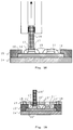
- the module 10 is placed over a hot plate 14 and firmly affixed thereto by means of a clamping device, typically a frame 15.
- a clamping device typically a frame 15.
- the hot plate 14 is part of a pull machine (for instance, model 1122 sold by INSTRON LTD, Buckinghamshire, UK).
- a pulling device is schematically represented in Fig. 1A by a stud 16 mounted on a pull head.
- the temperature of the hot plate 14 can be accurately controlled and regulated as standard.
- a small amount of a quick curing glue is applied over the chip top surface and forms a glob 17 thereon.
- a cyanate-ester based glue such as the JM7000 sold by JOHNSON MATTHEY, London, UK, is adequate in all respects.
- Its glass transition temperature Tg2 is equal to 240°C.
- the thickness of the glue is from about 10 ⁇ m to about 150 ⁇ m and is preferably equal to 100 ⁇ m.
- the chip 11 selected for being removed is aligned with the stud 16 e.g. by means of an X/Y table supporting the hot plate 14.
- the stud 16 is lowered to enter into contact with the glob 17.
- the hot plate 14 is raised to a temperature T1 (cure temperature) and a duration sufficient to fully cure the glue forming glob 17 providing thereby a very strong bond between the stud 16 extremity and the chip 11.
- a temperature T1 equals to 160 ⁇ C is adequate in that respect.
- the stud 16 is obtained by sawing a stainless steel rod into 3 cm long pieces.
- the section of the rod is in the particular case of such wire-bonded MCM modules slightly smaller than the size of the chip 11 by about 1 mm over the chip periphery.
- a 5x9 mm2 section stud is used for a 6x10 mm2 chip.
- This clearance allows to form a fillet of glue all around the stud 16 extremity at the chip periphery that coats the wires.
- the surface of the stud 16 that comes into contact with the top or upward surface of the chip 11 is preferably sand-blasted to improve adhesion therewith.
- the hot plate 14 is then raised to a temperature T2 (removal temperature) at least equal but preferably above the glass transition temperature Tg1 of the adhesive material to reduce the coupling between the chip 11 and the substrate 10.
- T2 glass transition temperature
- Tg1 glass transition temperature
- Tg1 glass transition temperature of the adhesive material
- Fig. 1A For small chips, usage of a pull machine is no longer mandatory. Designing a stud matching the small chip size could become an expensive process. Thus, the manual removal method described below in conjunction with Fig. 1B is recommended, but the automatic tooling described by reference to Fig. 1A could still be employed. The other operating conditions are substantially the same. Similar elements referenced in Fig. 1A will bear the same reference but will be differentiated by a prime. Now turning to Fig.1B, the frame 15' is provided with pins 18 that are adapted to receive a mask 19 that has the desired hole pattern corresponding to the chip array. In this case, the stud 16 simply consists of a small tube referenced 16'.
- An annular stud is preferred in this context because it increases the contacting surface between the stud and the glue material.
- dispense needles for in stance, models GP sold by EFD Inc., East Buffalo, RI, USA, with internal diameters ranging from .1 to 1.5 mm, that have demonstrated their capability of removing chips having sizes comprised between 1x1 mm2 and 5x5 mm2.
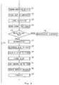
- FIG. 2 The basic steps describing the standard chip attachment process and the chip removal process pursuant to the present invention are schematically illustrated by flow-chart 20 in Fig. 2.
- the adhesive material is first dispensed at the surface of the substrate at the chip site (box 21), then the chip is correctly placed thereon (box 22). The adhesive is cured (box 23). Next, the wires are bonded to the I/O pads and the metal lands (box 24). The substrate is submitted to electrical tests to determine its operability. If tested “good”, the substrate is encapsulated (box 26). If some chip is tested "bad”, a diagnostic of the failure is per formed (box 27). The above described procedure is standard. Now, the steps of chip removal according to the present invention will be described.
- a glob of glue is dispensed on the top surface of the defective chip (box 28).
- the stud is lowered and firmly applied onto the glob of glue (box 29).
- the glue is cured (box 30).
- the wires are encapsulated in the glue.
- the substrate is heated and the stud is lifted up (box 31).
- the adhesive residues (if any) are removed (box 32) and the substrate is inspected (box 33).
- the reworked substrate is then submitted again to the steps described above for a new pass as illustrated in Fig. 2 by loop 34.
Abstract
Description
Claims (12)
- Method for removing a selected semiconductor chip (11) adhesively attached to the substrate (10) of an electronic module comprising the steps of:placing the substrate (10) on a plate (14) and clamping it thereon;applying a small amount of a quick curing glue onto the exposed surface of the said selected chip to be removed to form a glob (17);aligning a stud (16) with said chip, then lowering it to contact the glob atop the chip;heating the substrate to a first temperature (T1) to cure the glue material providing thereby a strong bond between the stud extremity and the chip;heating the substrate to a second temperature (T2) to reduce the adhesion between the chip and the substrate; and,pulling the stud to release said selected chip from the substrate.
- The method of claim 1 wherein said electronic module is a MCM module of the wire-bonded type wherein connecting wires ensure the electrical interconnection between the chip pads and the metal lands formed on the substrate surface.
- The method of claim 2 wherein the glue also encapsulates the connecting wires (13).
- The method of claim 3 wherein the stud section is less than the surface of the chip to produce a fillet of glue at the pheriphery of the chip for connecting wire encapsulation purposes.
- The method of any above claim wherein the adhesive material is an epoxy material and the glue material is a cyanate-ester based material.
- The method of claim 5 wherein the second temperature is equal or greater than the glass transition temperature of the epoxy material.
- The method of claim 6 wherein said first and second temperatures T1 and T2 are equal to about 160°C and 180°C respectively.
- The method of claim 6 wherein said first and second temperatures T1 and T2 are equal to about 160°C.
- The method of any above claim wherein said stud is obtained by sawing a stainless steel rod.
- The method of claim 9 wherein the extremity of the stud that is adjacent to the chip is sand-blasted for better adhesion.
- The method of any above claim 1 to 8 wherein said stud consists of a dispense needle to adapt to small chips having a size in the range of 1x1 to 5x5 mm2.
- The method of any above claim wherein the pull speed is in the range of 10 mm/mn.
Priority Applications (1)
| Application Number | Priority Date | Filing Date | Title |
|---|---|---|---|
| EP96480106A EP0843352A1 (en) | 1996-11-15 | 1996-11-15 | Method for removing a semiconductor chip bonded to a wire-bonded multichip module |
Applications Claiming Priority (1)
| Application Number | Priority Date | Filing Date | Title |
|---|---|---|---|
| EP96480106A EP0843352A1 (en) | 1996-11-15 | 1996-11-15 | Method for removing a semiconductor chip bonded to a wire-bonded multichip module |
Publications (1)
| Publication Number | Publication Date |
|---|---|
| EP0843352A1 true EP0843352A1 (en) | 1998-05-20 |
Family
ID=8225462
Family Applications (1)
| Application Number | Title | Priority Date | Filing Date |
|---|---|---|---|
| EP96480106A Withdrawn EP0843352A1 (en) | 1996-11-15 | 1996-11-15 | Method for removing a semiconductor chip bonded to a wire-bonded multichip module |
Country Status (1)
| Country | Link |
|---|---|
| EP (1) | EP0843352A1 (en) |
Cited By (2)
| Publication number | Priority date | Publication date | Assignee | Title |
|---|---|---|---|---|
| DE10125905C1 (en) * | 2001-05-28 | 2002-11-28 | Infineon Technologies Ag | Releasable coupling between IC chip and carrier uses interlocking mechanical coupling elements provided by IC chip and carrier |
| WO2020123038A1 (en) * | 2018-12-10 | 2020-06-18 | Applied Materials, Inc. | Attachment feature removal from photomask in extreme ultraviolet lithography application |
Citations (3)
| Publication number | Priority date | Publication date | Assignee | Title |
|---|---|---|---|---|
| WO1991003835A1 (en) * | 1989-09-05 | 1991-03-21 | Hughes Aircraft Company | Reworkable epoxy die-attach adhesive |
| WO1992008247A1 (en) * | 1990-10-24 | 1992-05-14 | Johnson-Matthey Inc. | Rapid-curing adhesive formulation for semiconductor devices |
| EP0600289A2 (en) * | 1992-11-27 | 1994-06-08 | Matsushita Electric Industrial Co., Ltd. | Semiconductor chip removal process and apparatus |
-
1996
- 1996-11-15 EP EP96480106A patent/EP0843352A1/en not_active Withdrawn
Patent Citations (3)
| Publication number | Priority date | Publication date | Assignee | Title |
|---|---|---|---|---|
| WO1991003835A1 (en) * | 1989-09-05 | 1991-03-21 | Hughes Aircraft Company | Reworkable epoxy die-attach adhesive |
| WO1992008247A1 (en) * | 1990-10-24 | 1992-05-14 | Johnson-Matthey Inc. | Rapid-curing adhesive formulation for semiconductor devices |
| EP0600289A2 (en) * | 1992-11-27 | 1994-06-08 | Matsushita Electric Industrial Co., Ltd. | Semiconductor chip removal process and apparatus |
Cited By (5)
| Publication number | Priority date | Publication date | Assignee | Title |
|---|---|---|---|---|
| DE10125905C1 (en) * | 2001-05-28 | 2002-11-28 | Infineon Technologies Ag | Releasable coupling between IC chip and carrier uses interlocking mechanical coupling elements provided by IC chip and carrier |
| US6756540B2 (en) | 2001-05-28 | 2004-06-29 | Infineon Technologies Ag | Self-adhering chip |
| WO2020123038A1 (en) * | 2018-12-10 | 2020-06-18 | Applied Materials, Inc. | Attachment feature removal from photomask in extreme ultraviolet lithography application |
| US10928724B2 (en) | 2018-12-10 | 2021-02-23 | Applied Materials, Inc. | Attachment feature removal from photomask in extreme ultraviolet lithography application |
| CN113169047A (en) * | 2018-12-10 | 2021-07-23 | 应用材料公司 | Removal of attachment features from a photomask in extreme ultraviolet lithography applications |
Similar Documents
| Publication | Publication Date | Title |
|---|---|---|
| US5007576A (en) | Testable ribbon bonding method and wedge bonding tool for microcircuit device fabrication | |
| US6429028B1 (en) | Process to remove semiconductor chips from a plastic package | |
| CN100395886C (en) | Semiconductor device manufacturing method | |
| KR20070098623A (en) | Manufacturing method of a semiconductor device | |
| KR0129119B1 (en) | Semiconductor chip removal process and apparatus | |
| JPH0582616A (en) | Method and apparatus for connecting circuit chip and temporary carrier for burn-in test | |
| JP3451987B2 (en) | Functional element, substrate for mounting functional element, and method of connecting them | |
| JP3262728B2 (en) | Semiconductor device and manufacturing method thereof | |
| JPH0870081A (en) | Ic package and its manufacture | |
| JPH06151701A (en) | Manufacture of semiconductor device | |
| EP0843352A1 (en) | Method for removing a semiconductor chip bonded to a wire-bonded multichip module | |
| JP3531580B2 (en) | Bonding method | |
| US5528157A (en) | Integrated circuit package for burn-in and testing of an integrated circuit die | |
| JP2002110736A (en) | Semiconductor device and its manufacturing method | |
| US6989334B2 (en) | Manufacturing method of a semiconductor device | |
| JP5054954B2 (en) | Manufacturing method of semiconductor device | |
| US7284686B2 (en) | Mounting method of bump-equipped electronic component and mounting structure of the same | |
| US6881593B2 (en) | Semiconductor die adapter and method of using | |
| JP3319455B2 (en) | Method for manufacturing semiconductor device | |
| JP2706405B2 (en) | Semiconductor chip mounting method | |
| JPH09181122A (en) | Method for manufacturing semiconductor device | |
| JP2699784B2 (en) | Semiconductor chip removal method | |
| JP2001244298A (en) | Method of flip chip bonding | |
| JP2821777B2 (en) | Flip chip IC and manufacturing method thereof | |
| US11393759B2 (en) | Alignment carrier for interconnect bridge assembly |
Legal Events
| Date | Code | Title | Description |
|---|---|---|---|
| PUAI | Public reference made under article 153(3) epc to a published international application that has entered the european phase |
Free format text: ORIGINAL CODE: 0009012 |
|
| AK | Designated contracting states |
Kind code of ref document: A1 Designated state(s): CH DE FR GB IT LI |
|
| AX | Request for extension of the european patent |
Free format text: AL;LT;LV;RO;SI |
|
| 17P | Request for examination filed |
Effective date: 19981120 |
|
| AKX | Designation fees paid |
Free format text: DE FR GB |
|
| RBV | Designated contracting states (corrected) |
Designated state(s): DE FR GB |
|
| RBV | Designated contracting states (corrected) |
Designated state(s): DE DK ES FR GB |
|
| RBV | Designated contracting states (corrected) |
Designated state(s): CH DE FR GB IT LI |
|
| STAA | Information on the status of an ep patent application or granted ep patent |
Free format text: STATUS: THE APPLICATION IS DEEMED TO BE WITHDRAWN |
|
| 18D | Application deemed to be withdrawn |
Effective date: 20010601 |