EP0837504A2 - Partially or completely encapsulated ferroelectric device - Google Patents
Partially or completely encapsulated ferroelectric device Download PDFInfo
- Publication number
- EP0837504A2 EP0837504A2 EP97306287A EP97306287A EP0837504A2 EP 0837504 A2 EP0837504 A2 EP 0837504A2 EP 97306287 A EP97306287 A EP 97306287A EP 97306287 A EP97306287 A EP 97306287A EP 0837504 A2 EP0837504 A2 EP 0837504A2
- Authority
- EP
- European Patent Office
- Prior art keywords
- ferroelectric
- layer
- electrode
- top electrode
- forming
- Prior art date
- Legal status (The legal status is an assumption and is not a legal conclusion. Google has not performed a legal analysis and makes no representation as to the accuracy of the status listed.)
- Withdrawn
Links
- 239000003990 capacitor Substances 0.000 claims abstract description 107
- 238000001465 metallisation Methods 0.000 claims abstract description 73
- 238000000034 method Methods 0.000 claims abstract description 62
- 239000001257 hydrogen Substances 0.000 claims abstract description 38
- 229910052739 hydrogen Inorganic materials 0.000 claims abstract description 38
- UFHFLCQGNIYNRP-UHFFFAOYSA-N Hydrogen Chemical compound [H][H] UFHFLCQGNIYNRP-UHFFFAOYSA-N 0.000 claims abstract description 18
- 239000000463 material Substances 0.000 claims description 66
- 238000005530 etching Methods 0.000 claims description 51
- 230000015654 memory Effects 0.000 claims description 50
- 238000004519 manufacturing process Methods 0.000 claims description 28
- 239000000758 substrate Substances 0.000 claims description 26
- 238000007373 indentation Methods 0.000 claims description 17
- 230000003247 decreasing effect Effects 0.000 claims description 16
- XUIMIQQOPSSXEZ-UHFFFAOYSA-N Silicon Chemical compound [Si] XUIMIQQOPSSXEZ-UHFFFAOYSA-N 0.000 claims description 12
- 229910052710 silicon Inorganic materials 0.000 claims description 12
- 239000010703 silicon Substances 0.000 claims description 12
- 238000002161 passivation Methods 0.000 claims description 9
- 230000032683 aging Effects 0.000 claims 4
- 230000035945 sensitivity Effects 0.000 abstract description 19
- 238000005538 encapsulation Methods 0.000 abstract description 4
- BASFCYQUMIYNBI-UHFFFAOYSA-N platinum Chemical compound [Pt] BASFCYQUMIYNBI-UHFFFAOYSA-N 0.000 description 42
- 229910052697 platinum Inorganic materials 0.000 description 21
- 150000002431 hydrogen Chemical class 0.000 description 20
- 239000011521 glass Substances 0.000 description 19
- 229910052451 lead zirconate titanate Inorganic materials 0.000 description 19
- HFGPZNIAWCZYJU-UHFFFAOYSA-N lead zirconate titanate Chemical compound [O-2].[O-2].[O-2].[O-2].[O-2].[Ti+4].[Zr+4].[Pb+2] HFGPZNIAWCZYJU-UHFFFAOYSA-N 0.000 description 19
- 229910052751 metal Inorganic materials 0.000 description 19
- 239000002184 metal Substances 0.000 description 19
- 230000008569 process Effects 0.000 description 19
- 238000011084 recovery Methods 0.000 description 18
- 238000010438 heat treatment Methods 0.000 description 15
- WFKWXMTUELFFGS-UHFFFAOYSA-N tungsten Chemical compound [W] WFKWXMTUELFFGS-UHFFFAOYSA-N 0.000 description 12
- 229910052721 tungsten Inorganic materials 0.000 description 12
- 239000010937 tungsten Substances 0.000 description 12
- XKRFYHLGVUSROY-UHFFFAOYSA-N Argon Chemical compound [Ar] XKRFYHLGVUSROY-UHFFFAOYSA-N 0.000 description 10
- 239000005380 borophosphosilicate glass Substances 0.000 description 10
- 239000004065 semiconductor Substances 0.000 description 10
- QVGXLLKOCUKJST-UHFFFAOYSA-N atomic oxygen Chemical compound [O] QVGXLLKOCUKJST-UHFFFAOYSA-N 0.000 description 9
- 239000001301 oxygen Substances 0.000 description 9
- 229910052760 oxygen Inorganic materials 0.000 description 9
- 230000015556 catabolic process Effects 0.000 description 8
- 238000006731 degradation reaction Methods 0.000 description 8
- VNSWULZVUKFJHK-UHFFFAOYSA-N [Sr].[Bi] Chemical compound [Sr].[Bi] VNSWULZVUKFJHK-UHFFFAOYSA-N 0.000 description 5
- 229910052782 aluminium Inorganic materials 0.000 description 5
- XAGFODPZIPBFFR-UHFFFAOYSA-N aluminium Chemical compound [Al] XAGFODPZIPBFFR-UHFFFAOYSA-N 0.000 description 5
- 229910052786 argon Inorganic materials 0.000 description 5
- 229910052454 barium strontium titanate Inorganic materials 0.000 description 5
- 238000009792 diffusion process Methods 0.000 description 5
- ZAMOUSCENKQFHK-UHFFFAOYSA-N Chlorine atom Chemical compound [Cl] ZAMOUSCENKQFHK-UHFFFAOYSA-N 0.000 description 4
- VYPSYNLAJGMNEJ-UHFFFAOYSA-N Silicium dioxide Chemical compound O=[Si]=O VYPSYNLAJGMNEJ-UHFFFAOYSA-N 0.000 description 4
- RTAQQCXQSZGOHL-UHFFFAOYSA-N Titanium Chemical compound [Ti] RTAQQCXQSZGOHL-UHFFFAOYSA-N 0.000 description 4
- NRTOMJZYCJJWKI-UHFFFAOYSA-N Titanium nitride Chemical compound [Ti]#N NRTOMJZYCJJWKI-UHFFFAOYSA-N 0.000 description 4
- 239000000460 chlorine Substances 0.000 description 4
- 229910052801 chlorine Inorganic materials 0.000 description 4
- 150000004767 nitrides Chemical class 0.000 description 4
- 239000010409 thin film Substances 0.000 description 4
- 239000010936 titanium Substances 0.000 description 4
- 229910052719 titanium Inorganic materials 0.000 description 4
- YCKRFDGAMUMZLT-UHFFFAOYSA-N Fluorine atom Chemical compound [F] YCKRFDGAMUMZLT-UHFFFAOYSA-N 0.000 description 3
- 230000008901 benefit Effects 0.000 description 3
- 229910010293 ceramic material Inorganic materials 0.000 description 3
- 229910052731 fluorine Inorganic materials 0.000 description 3
- 239000011737 fluorine Substances 0.000 description 3
- 229910021420 polycrystalline silicon Inorganic materials 0.000 description 3
- 229920005591 polysilicon Polymers 0.000 description 3
- 238000000992 sputter etching Methods 0.000 description 3
- -1 SBT Inorganic materials 0.000 description 2
- 238000000137 annealing Methods 0.000 description 2
- 238000000151 deposition Methods 0.000 description 2
- 230000008021 deposition Effects 0.000 description 2
- 238000010586 diagram Methods 0.000 description 2
- 239000007772 electrode material Substances 0.000 description 2
- 230000005669 field effect Effects 0.000 description 2
- 239000007789 gas Substances 0.000 description 2
- 229910052741 iridium Inorganic materials 0.000 description 2
- GKOZUEZYRPOHIO-UHFFFAOYSA-N iridium atom Chemical compound [Ir] GKOZUEZYRPOHIO-UHFFFAOYSA-N 0.000 description 2
- 230000010287 polarization Effects 0.000 description 2
- 235000012239 silicon dioxide Nutrition 0.000 description 2
- 239000000377 silicon dioxide Substances 0.000 description 2
- 229910052581 Si3N4 Inorganic materials 0.000 description 1
- 238000009825 accumulation Methods 0.000 description 1
- 230000015572 biosynthetic process Effects 0.000 description 1
- 229910002115 bismuth titanate Inorganic materials 0.000 description 1
- 239000003989 dielectric material Substances 0.000 description 1
- HTXDPTMKBJXEOW-UHFFFAOYSA-N dioxoiridium Chemical compound O=[Ir]=O HTXDPTMKBJXEOW-UHFFFAOYSA-N 0.000 description 1
- 229910002112 ferroelectric ceramic material Inorganic materials 0.000 description 1
- 239000010408 film Substances 0.000 description 1
- 238000005247 gettering Methods 0.000 description 1
- 229910000457 iridium oxide Inorganic materials 0.000 description 1
- 230000007246 mechanism Effects 0.000 description 1
- 239000000203 mixture Substances 0.000 description 1
- 238000012986 modification Methods 0.000 description 1
- 230000004048 modification Effects 0.000 description 1
- 239000005022 packaging material Substances 0.000 description 1
- 238000005498 polishing Methods 0.000 description 1
- 230000009467 reduction Effects 0.000 description 1
- HQVNEWCFYHHQES-UHFFFAOYSA-N silicon nitride Chemical compound N12[Si]34N5[Si]62N3[Si]51N64 HQVNEWCFYHHQES-UHFFFAOYSA-N 0.000 description 1
- 239000000126 substance Substances 0.000 description 1
- TXEYQDLBPFQVAA-UHFFFAOYSA-N tetrafluoromethane Chemical compound FC(F)(F)F TXEYQDLBPFQVAA-UHFFFAOYSA-N 0.000 description 1
Images


Classifications
-
- H—ELECTRICITY
- H10—SEMICONDUCTOR DEVICES; ELECTRIC SOLID-STATE DEVICES NOT OTHERWISE PROVIDED FOR
- H10B—ELECTRONIC MEMORY DEVICES
- H10B53/00—Ferroelectric RAM [FeRAM] devices comprising ferroelectric memory capacitors
-
- H—ELECTRICITY
- H01—ELECTRIC ELEMENTS
- H01L—SEMICONDUCTOR DEVICES NOT COVERED BY CLASS H10
- H01L28/00—Passive two-terminal components without a potential-jump or surface barrier for integrated circuits; Details thereof; Multistep manufacturing processes therefor
- H01L28/40—Capacitors
- H01L28/55—Capacitors with a dielectric comprising a perovskite structure material
-
- H—ELECTRICITY
- H01—ELECTRIC ELEMENTS
- H01L—SEMICONDUCTOR DEVICES NOT COVERED BY CLASS H10
- H01L29/00—Semiconductor devices adapted for rectifying, amplifying, oscillating or switching, or capacitors or resistors with at least one potential-jump barrier or surface barrier, e.g. PN junction depletion layer or carrier concentration layer; Details of semiconductor bodies or of electrodes thereof ; Multistep manufacturing processes therefor
- H01L29/40—Electrodes ; Multistep manufacturing processes therefor
- H01L29/401—Multistep manufacturing processes
- H01L29/4011—Multistep manufacturing processes for data storage electrodes
- H01L29/40114—Multistep manufacturing processes for data storage electrodes the electrodes comprising a conductor-insulator-conductor-insulator-semiconductor structure
-
- H—ELECTRICITY
- H01—ELECTRIC ELEMENTS
- H01L—SEMICONDUCTOR DEVICES NOT COVERED BY CLASS H10
- H01L29/00—Semiconductor devices adapted for rectifying, amplifying, oscillating or switching, or capacitors or resistors with at least one potential-jump barrier or surface barrier, e.g. PN junction depletion layer or carrier concentration layer; Details of semiconductor bodies or of electrodes thereof ; Multistep manufacturing processes therefor
- H01L29/66—Types of semiconductor device ; Multistep manufacturing processes therefor
- H01L29/66007—Multistep manufacturing processes
- H01L29/66075—Multistep manufacturing processes of devices having semiconductor bodies comprising group 14 or group 13/15 materials
- H01L29/66227—Multistep manufacturing processes of devices having semiconductor bodies comprising group 14 or group 13/15 materials the devices being controllable only by the electric current supplied or the electric potential applied, to an electrode which does not carry the current to be rectified, amplified or switched, e.g. three-terminal devices
- H01L29/66409—Unipolar field-effect transistors
- H01L29/66477—Unipolar field-effect transistors with an insulated gate, i.e. MISFET
- H01L29/66825—Unipolar field-effect transistors with an insulated gate, i.e. MISFET with a floating gate
-
- H—ELECTRICITY
- H01—ELECTRIC ELEMENTS
- H01L—SEMICONDUCTOR DEVICES NOT COVERED BY CLASS H10
- H01L29/00—Semiconductor devices adapted for rectifying, amplifying, oscillating or switching, or capacitors or resistors with at least one potential-jump barrier or surface barrier, e.g. PN junction depletion layer or carrier concentration layer; Details of semiconductor bodies or of electrodes thereof ; Multistep manufacturing processes therefor
- H01L29/66—Types of semiconductor device ; Multistep manufacturing processes therefor
- H01L29/68—Types of semiconductor device ; Multistep manufacturing processes therefor controllable by only the electric current supplied, or only the electric potential applied, to an electrode which does not carry the current to be rectified, amplified or switched
- H01L29/76—Unipolar devices, e.g. field effect transistors
- H01L29/772—Field effect transistors
- H01L29/78—Field effect transistors with field effect produced by an insulated gate
- H01L29/78391—Field effect transistors with field effect produced by an insulated gate the gate comprising a layer which is used for its ferroelectric properties
-
- H—ELECTRICITY
- H10—SEMICONDUCTOR DEVICES; ELECTRIC SOLID-STATE DEVICES NOT OTHERWISE PROVIDED FOR
- H10B—ELECTRONIC MEMORY DEVICES
- H10B53/00—Ferroelectric RAM [FeRAM] devices comprising ferroelectric memory capacitors
- H10B53/30—Ferroelectric RAM [FeRAM] devices comprising ferroelectric memory capacitors characterised by the memory core region
Definitions
- This invention relates generally to ferroelectric capacitors and transistors. More particularly, the present invention relates to a technique and structure for preventing degradation in the electrical performance of ferroelectric capacitors and transistors.
- FIG. 1 A portion of a prior art integrated circuit ferroelectric memory cell 10 including a transistor and a ferroelectric capacitor is shown in FIG. 1.
- a silicon or other substrate 12 includes a diffused region 14, which forms part of a transistor used in the memory cell.
- a thick oxide layer 16 forms the substrate for the ferroelectric capacitor.
- the thick oxide layer 16 is patterned and etched to allow access to diffused region 14.
- the ferroelectric capacitor includes a platinum bottom electrode 18, a ferroelectric layer 20, typically PZT (lead zirconate titanate), and a platinum top electrode 22.
- a subsequent oxide layer 24 is deposited, which is patterned and etched, to provide access to diffused region 14, bottom electrode 18, and to top electrode 22
- a local interconnect layer 26 is deposited, patterned and etched, to provide a local interconnect 26A between top electrode 22 and diffused region 14, as well as metalization 26B for bottom electrode 18.
- ferroelectric materials particularly PZT
- PZT PZT
- One source of hydrogen can be found in the plastic packaging materials often used with integrated circuits.
- Another source of hydrogen can be found in the various oxide layers used in fabricating the ferroelectric capacitor or memory cell.
- a section 28 of memory cell 10 is shown in greater magnification in FIG. 2 to illustrate the problem of hydrogen sensitivity that exists within the prior art memory cell.
- Section 28 shows oxide layer 16, bottom electrode 18, ferroelectric layer 20, top electrode 22, oxide layer 24, and local interconnect 26A. Note particularly in FIG. 2 that there is an interface between oxide layer 24 and ferroelectric layer 20. The interface extends along the top surface and sides of ferroelectric layer 20.
- hydrogen is generated within oxide layer 24, which in turn is gradually absorbed by ferroelectric layer 20.
- the arrows shown in FIG. 2 show generally the probable path of hydrogen diffusion into the ferroelectric layer 20. Studies have shown that exposure to hydrogen gradually degrades the amount of switching charge produced by the ferroelectric capacitor. Over time, the exposure to hydrogen may destroy electrical switching performance altogether.
- capacitor fabricated as set forth herein can be used in a wide array of electronic products such as integrated circuit memories and other integrated circuits, RF/ID integrated circuits and cards, discrete devices, or any application in which improved electrical switching performance and resistance to hydrogen diffusion is desired.
- a ferroelectric capacitor includes a bottom electrode, a top electrode, and a ferroelectric layer located between the top and bottom electrodes that extends to completely encapsulate the top electrode, except for a contact hole to allow metalization of the top electrode.
- the total encapsulation of the top electrode reduces the sensitivity of the ferroelectric capacitor to hydrogen and thus improves electrical switching performance.
- a ferroelectric capacitor includes a bottom electrode and a ferroelectric layer formed on the bottom electrode.
- the ferroelectric layer is partially etched to form an indentation to receive a top electrode.
- a dielectric layer is formed over the ferroelectric layer, and includes a contact hole to allow metalization of the top electrode. The partial encapsulation of the top electrode also reduces the sensitivity of the ferroelectric capacitor to hydrogen.
- the ferroelectric layer in the capacitor can be fabricated using PZT, SBT, or other known ferroelectric materials.
- the ferroelectric capacitor can then be used in conjunction with a transistor to form a memory cell in an array of such cells.
- a first method of fabricating a ferroelectric capacitor according to the present invention includes the steps of: forming in sequence a bottom electrode layer, a first ferroelectric layer, and a top electrode layer; etching the top electrode layer to form a top electrode; forming a second ferroelectric layer over the first ferroelectric layer, thereby completely encapsulating the top electrode; etching the second ferroelectric layer; etching the first ferroelectric layer and the bottom electrode layer to form a bottom electrode; forming a dielectric layer over the etched first ferroelectric and second ferroelectric layers; etching a contact hole through the dielectric layer and the second ferroelectric layer to allow metalization of the top electrode; and etching a contact hole through the dielectric layer and the first ferroelectric layer to allow metalization of the bottom electrode.
- a second method of fabricating a ferroelectric capacitor according to the present invention includes the steps of: forming in sequence a bottom electrode layer, a first ferroelectric layer, and a top electrode layer; etching the top electrode layer to form a top electrode; etching the first ferroelectric layer; etching the bottom electrode layer to form a bottom electrode; forming a second ferroelectric layer over the first ferroelectric layer, thereby completely encapsulating the top electrode; etching the second ferroelectric layer so that the second ferroelectric layer overlaps the bottom electrode; forming a dielectric layer over the etched second ferroelectric layer; and etching contact holes through the dielectric layer and the second ferroelectric layer to allow metalization of the top and bottom electrodes.
- a third method of fabricating a ferroelectric capacitor according to the present invention includes the steps of: forming in sequence a bottom electrode layer, a first ferroelectric layer, and a top electrode layer; etching the top electrode layer to form a top electrode; etching the first ferroelectric layer; etching the bottom electrode layer to form a bottom electrode; forming a second ferroelectric layer over the first ferroelectric layer, thereby completely encapsulating the top electrode; forming a dielectric layer over the second ferroelectric layer; and etching contact holes through the dielectric layer and the second ferroelectric layer to allow metalization of the top and bottom electrodes.
- a fourth method of fabricating a ferroelectric capacitor according to the present invention includes the steps of: forming in sequence a bottom electrode layer, a first ferroelectric layer of a first thickness, and a top electrode layer; etching the top electrode layer to form a top electrode; etching the first ferroelectric layer; forming a second ferroelectric layer of a second thickness over the first ferroelectric layer, thereby completely encapsulating the top electrode; etching the second ferroelectric layer and the bottom electrode layer to form a bottom electrode; forming a dielectric layer over the etched second ferroelectric layer; and etching contact holes through the dielectric layer and the second ferroelectric layer to allow metalization of the top and bottom electrodes.
- a fifth method of fabricating a ferroelectric capacitor according to the present invention includes the steps of: forming in sequence a bottom electrode layer and a ferroelectric layer; partially etching the ferroelectric layer to form an indentation; forming a conformal top electrode layer over the ferroelectric layer; etching away the top electrode layer to form a top electrode in the indentation; etching the ferroelectric layer; etching the bottom electrode layer to form a bottom electrode; forming a dielectric layer over the etched ferroelectric layer; and etching contact holes through the dielectric layer to allow metalization of the top and bottom electrodes.
- a sixth method of fabricating a ferroelectric capacitor according to the present invention includes the steps of: forming a bottom electrode layer; etching the bottom electrode layer to form a bottom electrode; forming a ferroelectric layer over the bottom electrode; partially etching the ferroelectric layer to form an indentation; forming a conformal top electrode layer over the ferroelectric layer; etching away the top electrode layer to form a top electrode in the indentation; forming a dielectric layer over the ferroelectric layer; etching a contact hole through the dielectric layer to allow metalization of the top electrodes; and etching a contact hole through the dielectric layer and the ferroelectric layer to allow metalization of the bottom electrode.
- An integrated circuit ferroelectric memory cell having a bit line, a word line, and a plate line, fabricated according to the present invention includes: a silicon substrate or epitaxial region; a transistor formed in the substrate including first and second diffused regions, a thin gate oxide, and a gate forming the word line; a thick oxide layer formed on the substrate including contact holes to allow metalization of the first and second diffused regions; a ferroelectric capacitor formed on the thick oxide layer, the ferroelectric capacitor including a bottom electrode, a ferroelectric layer, and a top electrode, wherein the ferroelectric layer either partially or completely encapsulates the top electrode and includes a contact hole to allow metalization of the top electrode; a first dielectric layer formed over the thick oxide layer and the ferroelectric capacitor including contact holes to allow metalization of the first and second diffused regions, and the top and bottom electrodes of the ferroelectric capacitor; a first patterned metalization layer for contacting the first diffused region, for forming a local interconnect between the top electrode and the second diffused region,
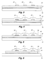
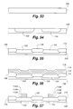
- FIGS. 3-9 sequential sectional views of a first ferroelectric capacitor process suitable for use in a ferroelectric memory having decreased hydrogen sensitivity are shown.
- a layer 16 of BPSG glass about 7000 Angstroms thick is deposited onto a silicon or other substrate (not shown). Any oxide, nitride, or other appropriate dielectric layer can be substituted for BPSG layer 16.
- a platinum bottom electrode layer 18 is subsequently deposited over BPSG glass layer 16 to a thickness of about 1750 Angstroms. While platinum is used for electrode layer 16, other known materials compatible with ferroelectric films can be used including iridium, iridium oxide, and the like.
- the bottom electrode layer 18 also includes a titanium adhesion layer about 200 Angstroms thick to facilitate the adhesion of the platinum bottom electrode layer 18 to BPSG glass layer 16.
- a first ferroelectric layer 20 is subsequently deposited over the bottom electrode layer 18 to a thickness of about 3000 Angstroms.
- the material used in ferroelectric layer 20 is ideally doped or undoped PZT (lead zirconate titanate), SBT (strontium bismuth tantalate), or any other known ferroelectric material suitable for use in thin film form.
- a first anneal is performed. The first anneal includes a 650 °C heat treatment for about five seconds, followed by an 850 °C heat treatment for about five seconds.
- a platinum top electrode layer 22 is subsequently deposited over the first ferroelectric layer 20 to a thickness of about 1750 Angstroms.
- the material used in top electrode layer 22 can be other than platinum as described above.
- Top electrode layer 22 is etched to form one or more top electrodes. Platinum is typically etched using a reactive-ion etch in an argon and chlorine atmosphere, although other gases can be used. Ion milling can be used as well as an alternative etching technique.
- the dimensions of the individual top electrodes can modified as desired from nominal dimensions of 1.5 x 1.5 microns, with a spacing of about three microns between top electrodes.
- a second anneal is performed. The second anneal includes a 650 °C heat treatment for about sixty minutes in an oxygen atmosphere.
- a second "cap" ferroelectric layer 30 about the same thickness (3000 Angstroms) as the first ferroelectric layer 20 is deposited over the first ferroelectric layer 20, thereby completely encapsulating the top electrodes 22.
- the material used in the second ferroelectric layer 30 is also ideally doped or undoped PZT (lead zirconate titanate), SBT (strontium bismuth tantalate), or any other known ferroelectric material suitable for use in thin film form.
- the first and second ferroelectric layers need not be the same ferroelectric material, since the second layer is used for its resistance to hydrogen diffusion or hydrogen "gettering" properties and not specifically for its ferroelectric properties.
- an optional third anneal can be performed.
- the optional third anneal includes a 650 °C heat treatment for about sixty minutes in an oxygen atmosphere.
- the second ferroelectric layer 30 is etched according to the same etching method as set forth for the first ferroelectric layer 20.
- the second ferroelectric layer 30 is etched to leave a reasonable overlap of the top electrodes 22, about 1.5 to 2.0 microns.
- the first ferroelectric layer 20 and the bottom electrode layer 18 are simultaneously etched to define the dimensions of a bottom electrode. As can be seen in FIG. 6, one end of the bottom electrode 18 is etched to allow sufficient room for an eventual bottom electrode contact. The other end of bottom electrode 18 is etched to the same dimensions as the second ferroelectric layer 30.
- the first ferroelectric layer 20 and the bottom electrode layer 18 are simultaneously etched using a reactive-ion etch in an argon and carbon tetrafluoride atmosphere, although other gases can be used. Ion milling can also be used as an alternative etching technique.
- an optional first recovery anneal can be performed.
- the optional first recovery anneal includes a 550 °C heat treatment for about sixty minutes in an oxygen atmosphere.
- a PTEOS glass dielectric layer 24 is deposited over the etched first ferroelectric and second ferroelectric layers 20 and 30 to a thickness of about 5000 Angstroms. Other dielectric layers can be used for dielectric layer 24.
- contact holes are etched to provide access of the top and bottom electrodes 22 and 18.
- Contact hole 32 provides access to bottom electrode 18, and contact holes 34 provide access to top electrodes 22.
- Contact holes 34 are etched through the dielectric layer 24 and the second ferroelectric layer 30 to allow metalization of the top electrodes.
- Contact hole 32 is etched through the dielectric layer 24 and the first ferroelectric layer 20 to allow metalization of bottom electrode 18. Note that the contact holes 32 and 34 are ideally etched in two steps. The first etching step removes the dielectric layer 24 in the contact holes.
- the dielectric oxide material can be etched away using a fluorine-based wet or dry etch. It is desirable that a sloped profile is etched into the contact holes.
- the remaining ferroelectric material in the contact hole is etched away according to the ferroelectric etch described above. Note in FIG. 8 that contact holes 32 and 34 are etched through about the same thickness of material, i.e. 5000 Angstroms of glass plus 3000 Angstroms of ferroelectric material. Therefore, the etching of contact holes 32 and 34 can be performed simultaneously.
- an optional second recovery anneal can be performed. The optional second recovery anneal includes a 550 °C heat treatment for about sixty minutes in an oxygen atmosphere.
- contact holes 32 and 34 are metalized to provide electrical access to bottom electrode 18 and top electrodes 22.
- a titanium nitride local interconnect metalization layer is deposited to a thickness of about 800 Angstroms and etched to form a metal contact 36 for bottom electrode 18 and a metal contact 38 for each of the top electrodes 22.
- the full metalization scheme showing subsequent oxide and metalization layers for a ferroelectric memory cell is shown in FIG. 52, although other metalization schemes can be used.
- a titanium layer about 1500 Angstroms thick followed by an aluminum layer of about 8000 Angstroms thick can be used to form metal contacts 36 and 38.
- Other metalization techniques can be used as well after the titanium nitride layer has been deposited.
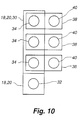
- FIG. 10 A plan view of the capacitor structure described above with respect to FIGS. 3-9 is shown in FIG. 10.
- the bottom electrode 18 and first ferroelectric layer 20 are shown as coincident layers forming a first rectangle.
- a second, smaller rectangle is formed of the bottom electrode 18, the first ferroelectric layer 20, and the second ferroelectric layer 30.
- the contact holes to the bottom and top electrodes 32 and 34 are shown as circular features.
- the local interconnect metal contact straps 38 that contact the top electrodes 22 are shown as individual rectangles overlapping contact holes 34 and 40.
- Contact holes 40 are not shown in FIGS. 3-9 but represent a contact to another structure such as the diffused region of a transistor as is shown in FIG. 52.
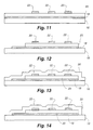
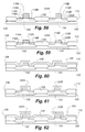
- FIGS. 11-17 sequential sectional views of a second ferroelectric capacitor process suitable for use in a ferroelectric memory having decreased hydrogen sensitivity are shown.
- FIG. 11 is the same sectional view as FIG. 3, showing the sequential deposition of a thick glass layer 16, a bottom electrode layer 18, a first ferroelectric layer 20, and a top electrode layer 22 All of the thicknesses and materials described above are the same in FIG. 11.
- a first anneal can be performed after the first ferroelectric layer 18 is deposited.
- the platinum top electrode layer 22 is etched to form individual top electrodes 22.
- a second anneal can be performed after the top electrodes 22 are etched.
- the first ferroelectric layer 20 is etched with some lateral overlap of the etched top electrodes 20.
- the bottom electrode layer 18 is etched to define the dimensions of a bottom electrode. As can be seen in FIG. 12, one end of the bottom electrode 18 is etched to allow sufficient room for the eventual bottom electrode contact. The other end of bottom electrode 18 is etched to the same dimensions as the first ferroelectric layer 20.
- the etching techniques for bottom electrode 18 and first ferroelectric layer 20 are as described above with reference to FIGS. 3-11.
- an optional first recovery anneal can be performed.
- the optional first recovery anneal includes a 550 °C heat treatment for about sixty minutes in an oxygen atmosphere.
- a second "cap" ferroelectric layer 30 about the same thickness (3000 Angstroms) as the first ferroelectric layer 20 is deposited over the first ferroelectric layer 20, thereby completely encapsulating the top electrodes 22.
- an optional third anneal can be performed.
- the optional third anneal includes a 650 °C heat treatment for about sixty minutes in an oxygen atmosphere.
- the second ferroelectric layer 30 is etched according to the same etching method as set forth for the first ferroelectric layer 20.
- the second ferroelectric layer 30 is etched to leave a reasonable overlap of the bottom electrode 18, about 1.5 to 2.0 microns.
- an optional second recovery anneal can be performed.
- a PTEOS glass dielectric layer 24 is deposited over the etched second ferroelectric layers 30 to a thickness of about 5000 Angstroms.
- contact holes are etched to provide access of the top and bottom electrodes 22 and 18.
- Contact hole 32 provides access to bottom electrode 18, and contact holes 34 provide access to top electrodes 22.
- both contact holes 34 and 36 are etched through the dielectric layer 24 and the second ferroelectric layer 30 to allow metalization of the top and bottom electrodes.
- the thickness of contact holes 34 and 36 is the same since they are etched through the same thickness of material.
- Contact holes 32 and 34 are ideally simultaneously etched in two steps to remove the dielectric oxide material and then the remaining ferroelectric material. The type of etch used in the same as described with reference to FIG. 8. After contact holes 32 and 34 are etched, an optional second recovery anneal can be performed.
- contact holes 32 and 34 are metalized to provide electrical access to bottom electrode 18 and top electrodes 22.
- a titanium nitride local interconnect metalization layer is deposited to a thickness of about 800 Angstroms and etched to form a metal contact 36 for bottom electrode 18 and a metal contact 38 for each of the top electrodes 22.
- the full metalization scheme showing subsequent oxide and metalization layers for a ferroelectric memory cell is shown in FIG. 52, although other metalization schemes can be used.
- FIG. 18 A plan view of the capacitor structure described above with respect to FIGS. 11-17 is shown in FIG. 18.
- the bottom electrode 18 is shown as forming a first rectangle.
- a second, smaller rectangle is formed of the bottom electrode 18 and the first ferroelectric layer 20.
- the second ferroelectric layer 30 is shown as a dashed rectangle overlapping the bottom electrode 18.
- the contact holes to the bottom and top electrodes 32 and 34 are shown as circular features.
- the local interconnect metal contact straps 38 that contact the top electrodes 22 are shown as individual rectangles overlapping contact holes 34 and 40.
- Contact holes 40 are not shown in FIGS. 11-17 but represent a contact to another structure such as the diffused region of a transistor as is shown in FIG. 52.
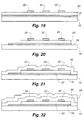
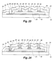
- FIGS. 19-24 sequential sectional views of a third ferroelectric capacitor process suitable for use in a ferroelectric memory having decreased hydrogen sensitivity are shown.
- FIGS. 19-21 are identical to previously described FIGS. 11-13 both in sectional views, material, etching, and annealing steps.
- FIG. 19 shows a thick glass layer 16, a bottom electrode layer 18, a first ferroelectric layer 20, and a top electrode layer 22 formed in sequence, wherein the top electrode layer 22 is etched to form individual top electrodes 22.
- FIG. 20 shows the etching of the first ferroelectric layer 20 and the etching of the bottom electrode layer 18 to form a bottom electrode.
- a second "cap" ferroelectric layer 30 about the same thickness (3000 Angstroms) as the first ferroelectric layer 20 is deposited over the first ferroelectric layer 20, thereby completely encapsulating the top electrodes 22.
- a first anneal is performed after the ferroelectric layer 20 is deposited, a second anneal is performed after the top electrode layer 22 is etched, and an optional third anneal is performed after the second ferroelectric layer 30 is deposited.
- a optional first recovery anneal is performed after the first ferroelectric layer 20 and bottom electrode layer 18 have been etched.
- a PTEOS glass dielectric layer 24 is deposited over the unetched second ferroelectric layer 30 to a thickness of about 5000 Angstroms.
- contact holes are etched to provide access of the top and bottom electrodes 22 and 18.
- Contact hole 32 provides access to bottom electrode 18, and contact holes 34 provide access to top electrodes 22.
- both contact holes 34 and 36 are etched through the dielectric layer 24 and the second ferroelectric layer 30 to allow metalization of the top and bottom electrodes.
- the thickness of contact holes 34 and 36 is the same since they are etched through the same thickness of material.
- Contact holes 32 and 34 are ideally simultaneously etched in two steps to remove the dielectric oxide material and then the remaining ferroelectric material. The type of etch used in the same as described with reference to FIG. 8.
- a second optional recovery anneal can be performed after contact holes 32 and 34 have been opened.
- contact holes 32 and 34 are metalized to provide electrical access to bottom electrode 18 and top electrodes 22.
- a titanium nitride local interconnect metalization layer is deposited to a thickness of about 800 Angstroms and etched to form a metal contact 36 for bottom electrode 18 and a metal contact 38 for each of the top electrodes 22.
- the full metalization scheme showing subsequent oxide and metalization layers for a ferroelectric memory cell is shown in FIG. 52, although other metalization schemes can be used.
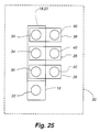
- FIG. 25 A plan view of the capacitor structure described above with respect to FIGS. 19-24 is shown in FIG. 25.
- the bottom electrode 18 is shown as forming a first rectangle.
- a second, smaller rectangle is formed of the bottom electrode 18 and the first ferroelectric layer 20.
- the second ferroelectric layer 30 is shown as a dashed rectangle overlapping the bottom electrode 18 by a wide margin. The wide margin shown is meant to convey the unetched, continuous extent of the second ferroelectric layer 30.
- the contact holes to the bottom and top electrodes 32 and 34 are shown as circular features.
- the local interconnect metal contact straps 38 that contact the top electrodes 22 are shown as individual rectangles overlapping contact holes 34 and 40. Contact holes 40 are not shown in FIGS. 19-24 but represent a contact to another structure such as the diffused region of a transistor as is shown in FIG. 52.
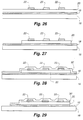
- FIGS. 26-32 sequential sectional views of a fourth ferroelectric capacitor process suitable for use in a ferroelectric memory having decreased hydrogen sensitivity are shown.
- the fourth ferroelectric capacitor process described below allows the thickness of the second ferroelectric layer 30 to be different from the first ferroelectric layer 20, if desired.
- FIG. 26 is the same as previously described FIGS. 3, 11, and 19.
- a first anneal is performed after the first ferroelectric layer 20 is deposited, and a second anneal is performed after the top electrode layer 22 is etched.
- FIG. 27 only the first ferroelectric layer 20 is etched to a reasonable overlap of the etched top electrodes 22.
- the bottom electrode layer 18 remains unetched in FIG. 27.
- An optional first recovery anneal is performed after the first ferroelectric layer 20 is etched.
- a second "cap" ferroelectric layer 30' of a different thickness (less than or greater than 3000 Angstroms) from the first ferroelectric layer 20 is deposited over the first ferroelectric layer 20, thereby completely encapsulating the top electrodes 22.
- a less thick second ferroelectric layer 30' is desirable since less material is used, it is easier to etch, more planar, and for other processing reasons. However, if desired, the same or a thicker ferroelectric layer 30' can be used.
- the material used for the second ferroelectric layer 30' is the same as described above, and can be different than the material used in the first ferroelectric layer 20.
- An optional third anneal can be performed after the second ferroelectric layer 30' is deposited.
- the second ferroelectric layer 30' and the bottom electrode layer 18 are simultaneously etched to form a bottom electrode.
- an optional second recovery anneal can be performed.
- a PTEOS glass dielectric layer 24 is deposited over the etched second ferroelectric layer 30' to a thickness of about 5000 Angstroms.
- contact holes are etched to provide access of the top and bottom electrodes 22 and 18.
- Contact hole 32 provides access to bottom electrode 18, and contact holes 34 provide access to top electrodes 22.
- both contact holes 34 and 36 are etched through the dielectric layer 24 and the second ferroelectric layer 30' to allow metalization of the top and bottom electrodes.
- the thickness of contact holes 34 and 36 is the same since they are etched through the same thickness of material.
- Contact holes 32 and 34 are ideally simultaneously etched in two steps to remove the dielectric oxide material and then the remaining ferroelectric material. The type of etch used in the same as described with reference to FIG. 8. After contact holes 32 and 34 have been etched, an optional third recovery anneal can be performed.
- contact holes 32 and 34 are metalized to provide electrical access to bottom electrode 18 and top electrodes 22.
- the full metalization scheme showing subsequent oxide and metalization layers for a ferroelectric memory cell is shown in FIG. 52, although other metalization schemes can be used.
- a plan view of the capacitor structure described above with respect to FIGS. 26-32 is not shown, but is similar to the plan view shown in FIG. 18. The one difference is that the second ferroelectric layer 30' does not overlap the bottom electrode 18, but is coincident thereto.
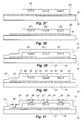
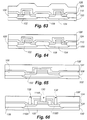
- FIGS. 33-41 sequential sectional views of a fifth ferroelectric capacitor process suitable for use in a ferroelectric memory having decreased hydrogen sensitivity are shown.
- a layer 16 of BPSG glass about 7000 Angstroms thick is deposited onto a silicon or other substrate (not shown).
- a platinum bottom electrode layer 18 is subsequently deposited over BPSG glass layer 16 to a thickness of about 1750 Angstroms.
- the bottom electrode layer 18 also includes a titanium adhesion layer about 200 Angstroms thick to facilitate the adhesion of the platinum bottom electrode layer 18 to BPSG glass layer 16.
- a ferroelectric layer 20 is subsequently deposited over the bottom electrode layer 18 to a thickness of about 3000 Angstroms.
- the material used in ferroelectric layer 20 is ideally doped or undoped PZT (lead zirconate titanate), SBT (strontium bismuth tantalate), or any other known ferroelectric material suitable for use in thin film form.
- the ferroelectric layer 20 is partially etched to form one or more indentations 42.
- Indentations 42 should be etched to a sufficient depth to completely receive the top electrodes as is explained in further detail below.
- the etching technique used is the same reactive-ion etch used in etching the ferroelectric layers.
- a first anneal is performed. The first anneal includes a 650 °C heat treatment for about five seconds, followed by an 850 °C heat treatment for about five seconds.
- a platinum top electrode layer 22 is subsequently deposited over the ferroelectric layer 20 to a thickness of about 1750 Angstroms.
- the top electrode layer 22 is conformal and thus fills in each of the indentations 42.
- the top electrode layer 22 is etched away to form one or more top electrodes in indentations 42.
- Platinum is typically etched using a reactive-ion etch in an argon and chlorine atmosphere.
- Alternative etching techniques include ion milling or chemical mechanical polishing (CMP).
- CMP chemical mechanical polishing
- the dimensions of the individual top electrodes can modified as desired from nominal dimensions of 1.5 x 1.5 microns, with a spacing of about three microns between top electrodes.
- a second anneal is performed.
- the second anneal includes a 650 °C heat treatment for about sixty minutes in an oxygen atmosphere.
- the ferroelectric layer 20 is etched to leave a reasonable lateral overlap of the top electrodes 22.
- the bottom electrode layer 18 is etched to define the dimensions of a bottom electrode. As can be seen in FIG. 38, one end of the bottom electrode 18 is etched to allow room for an eventual bottom electrode contact. The other end of bottom electrode 18 is etched to the same dimensions as the second ferroelectric layer 30.
- the bottom electrode layer 18 is etched using a reactive-ion etch in an argon and chlorine atmosphere. After the bottom electrode layer 18 is etched, an optional first recovery anneal can be performed.
- the optional first recovery anneal includes a 550 °C heat treatment for about sixty minutes in an oxygen atmosphere.
- a PTEOS glass dielectric layer 24 is deposited over the etched ferroelectric layer 20 to a thickness of about 5000 Angstroms.
- contact holes are etched to provide access of the top and bottom electrodes 22 and 18.
- Contact hole 32 provides access to bottom electrode 18, and contact holes 34 provide access to top electrodes 22.
- Contact holes 34 and 32 are etched through the dielectric layer 24 to allow metalization of the top electrodes and bottom electrodes 22 and 18. Note that the contact holes 32 and 34 are etched in a single etching step.
- the dielectric oxide material can be etched away using a fluorine-based wet or dry etch. It is desirable that a sloped profile is etched into the contact holes. Note in FIG. 40 that contact holes 32 and 34 are etched through about the same thickness of material, i.e. 5000 Angstroms of glass dielectric layer 24.
- a second optional recovery anneal can be performed after contact holes 32 and 34 are opened as previously described.
- contact holes 32 and 34 are metalized to provide electrical access to bottom electrode 18 and top electrodes 22 as previously described above.
- a pian view of the capacitor structure described above with respect to FIGS. 33-41 is similar to that shown in FIG. 10. The only difference is that there is no second level of ferroelectric material 30. The contours of the plan view, however, are the same.
- FIGS. 42-50 sequential sectional views of a sixth ferroelectric capacitor process suitable for use in a ferroelectric memory having decreased hydrogen sensitivity are shown.
- a layer 16 of BPSG glass about 7000 Angstroms thick is deposited onto a silicon or other substrate (not shown).
- a platinum bottom electrode layer 18 is subsequently deposited over BPSG glass layer 16 to a thickness of about 1750 Angstroms.
- the bottom electrode layer 18 also includes a titanium adhesion layer about 200 Angstroms thick to facilitate the adhesion of the platinum bottom electrode layer 18 to BPSG glass layer 16.
- bottom electrode layer 18 is etched to form a bottom electrode.
- a ferroelectric layer 20 is subsequently deposited over the bottom electrode 18 to a thickness of about 3000 Angstroms.
- the material used in ferroelectric layer 20 is ideally doped or undoped PZT (lead zirconate titanate), SBT (strontium bismuth tantalate), or any other known ferroelectric material suitable for use in thin film form.
- the ferroelectric layer 20 is partially etched to form one or more indentations 42.
- Indentations 42 should be etched to a sufficient depth to completely receive the top electrodes as is explained in further detail below.
- the etching technique used is the same reactive-ion etch used in etching the ferroelectric layers.
- a first anneal is performed. The first anneal includes a 650 °C heat treatment for about five seconds, followed by an 850 °C heat treatment for about five seconds.
- a platinum top electrode layer 22 is subsequently deposited over the ferroelectric layer 20 to a thickness of about 1750 Angstroms.
- the top electrode layer 22 is conformal and thus fills in each of the indentations 42.
- the top electrode layer 22 is etched away to form one or more top electrodes in indentations 42. Platinum is typically etched using a reactive-ion etch in an argon and chlorine atmosphere. The dimensions of the individual top electrodes can modified as desired from nominal dimensions of 1.5 x 1.5 microns, with a spacing of about three microns between top electrodes.
- a second anneal is performed. The second anneal includes a 650 °C heat treatment for about sixty minutes in an oxygen atmosphere.
- a PTEOS glass dielectric layer 24 is deposited over the etched ferroelectric layer 20 to a thickness of about 5000 Angstroms.
- contact holes are etched to provide access of the top and bottom electrodes 22 and 18.
- Contact hole 32 provides access to bottom electrode 18, and contact holes 34 provide access to top electrodes 22.
- Contact holes 34 are etched through the dielectric layer 24 to allow metalization of the top electrodes 22.
- Contact hole 32 is etched through dielectric layer 24 as well as ferroelectric layer 20. Note, therefore, that contact holes 32 and 34 are etched in two separate etching steps.
- the dielectric oxide material can be etched away using a fluorine-based wet or dry etch.
- the ferroelectric material is etched used a reactive-ion etch. It is desirable that a sloped profile is etched into the contact holes. An optional recovery anneal can be performed at this point in the process.
- contact holes 32 and 34 are metalized to provide electrical access to bottom electrode 18 and top electrodes 22 as previously described above.
- a plan view of the capacitor structure described above with respect to FIGS. 42-50 is similar to that shown in FIG. 25. The differences are that there is no second level of ferroelectric material 30, and the contour for ferroelectric material 20 should be removed.
- FIG. 51 a schematic diagram for a typical non-volatile ferroelectric memory is shown having a transistor 52 coupled to a ferroelectric capacitor 54.
- the configuration in FIG. 51 is known as a one-transistor, one-capacitor ferroelectric memory cell or "1T/1C" cell.
- One current node of the transistor 52 forms the bit line of the cell, and is designated 14, 46, 48 to correspond to regions in the integrated cell shown below in FIG. 52.
- the other current node of transistor 52 is coupled to ferroelectric capacitor 54 at node 56.
- the gate 15 of transistor 52 forms the word line of the memory cell.
- One end of capacitor 54 is coupled to transistor 52 at node 56, and the other end of capacitor 54 forms the plate line of the memory cell.
- the plate line node is designated 18, 36, 48 to correspond to regions in the integrated cell shown below in FIG. 52.
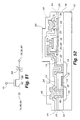
- FIG. 52 a sectional view of a completely metalized integrated circuit ferroelectric memory cell having a bit line, a word line, and a plate line is shown.
- the memory cell includes a silicon substrate or epitaxial region 12, and a transistor formed in the substrate 12 including first and second diffused regions 14, a thin gate oxide 13, and a gate 15 forming the word line.
- a thick oxide layer 16 is formed on the substrate 12 including contact holes to allow metalization of the first and second diffused regions 14. Note that in FIG. 52, the exact sequence for forming each of the various layers and contact holes within each layer is not fully described; the contact holes may actually be formed at a subsequent processing step.
- a ferroelectric capacitor is subsequently formed on the thick oxide layer 16, including a bottom electrode 18, a ferroelectric layer 20 + 30, and a top electrode 22, wherein the ferroelectric layer 20 + 30 either partially or completely encapsulates the top electrode 22.
- the ferroelectric layer 20 + 30 includes a contact hole to allow metalization of the top electrode 22.
- a first dielectric layer 24 is formed over the thick oxide layer 16 and the ferroelectric capacitor, including contact holes to allow metalization of the first and second diffused regions 14, and the top and bottom electrodes 22 and 18 of the ferroelectric capacitor.
- a first patterned metalization layer 36, 38, 46 is deposited for contacting the first diffused region 14 with metal contact 46, for forming a local interconnect 38 between the top electrode 22 and the second diffused region 14, and for metalizing the bottom electrode 36 with metal contact 36.
- a second dielectric layer 44 is formed over the first metalization layer 36, 38, 46 including contact holes to allow metalization of the first diffused region 14 and the bottom electrode 36.
- a second patterned metalization layer 48 contacts the first diffused region 14 and forms the bit line of the memory cell, and contacts the bottom electrode 18 to form the plate line of the memory cell.
- a passivation layer 50 is formed over the second metalization layer 48.
- first and second dielectric layers 24 and 44 are typically thin doped or undoped oxide layers, if greater resistance to hydrogen diffusion is required these layers can also be made of ferroelectric materials such as PZT or SBT. Still further, the passivation layer 50, while typically formed of silicon nitride or the like, can also be made from ferroelectric materials such as PZT or SBT. All three layers mentioned above can be fabricated of the same or different ferroelectric materials as desired, and not necessarily the same material as used in the ferroelectric layer of the ferroelectric capacitor. Further teachings regarding ferroelectric material passivation can be found in US Patent No.
- Ferroelectric FETs sometimes referred to as “MFSFETS”, which stands for “Metal-Ferroelectric-Semiconductor Field-Effect Transistors”, have been proposed as a memory element for a ferroelectric memory device.
- the ferroelectric FET is similar to a standard MOSFET, with the exception that the silicon dioxide gate dielectric layer is replaced with a ferroelectric gate dielectric layer. It is postulated that the ferroelectric FET could be an alternative to 1T-1C or 2T-2C memory cells in which separate switching devices and ferroelectric capacitors are used.
- ferroelectric gate dielectric layer In operation, polarization of the ferroelectric gate dielectric layer induces either accumulation or depletion/inversion of the channel underneath the gate region. Therefore, the ferroelectric FET is either off or on depending upon the ferroelectric polarization state and can thus be used as a memory element.
- Ferroelectric FETs are deemed to be a good alternative to standard ferroelectric memory cells since the read/write mechanism is nondestructive and the cell size of a single ferroelectric FET is small. To date, however, the problems inherent in the processing of ferroelectric FETs has prevented their widespread adoption.
- One problem with ferroelectric FETs is interdiffusion at the interface between the ferroelectric gate dielectric layer and the semiconductor layer where the channel is formed during deposition and/or during subsequent anneal cycles.
- Another problem of ferroelectric FETs is the degradation of the ferroelectric gate dielectric layer during subsequent processing steps. Once interdiffusion takes place a combination of two series capacitors is actually formed. A first capacitor is ferroelectric, but the second capacitor is non-ferroelectric and actually absorbs most of the applied external voltage. This results in a marked reduction in electrical performance and cannot be cured by subsequent thermal annealing.
- FIGS. 53-69 illustrate an improved fabrication method for forming a first embodiment of a ferroelectric FET including at least two source/drain regions and a ferroelectric gate structure in which the ferroelectric gate structure is encapsulated with a hydrogen-barrier cap layer distinct from the ferroelectric gate structure.
- the hydrogen-barrier cap layer both prevents degradation from hydrogen due to subsequent processing steps and minimizes or eliminates the need for subsequent recovery anneals. As a consequence, interdiffusion between the ferroelectric gate layer and the semiconductor region is also minimized.
- FIG. 53 a silicon or other semiconductor substrate or epitaxial layer 100 is shown in which the source/drain regions for the ferroelectric transistors are formed.
- diffused regions such as an N-well 102 and P-well 104 are diffused into the semiconductor substrate 100.
- field-oxide regions 106, 108, and 110 are thermally grown to a thickness of about 1 ⁇ m to electrically isolate wells 102 and 104.
- a ferroelectric gate dielectric layer 112 is formed to a thickness of about 500 to 5000 Angstroms.
- the ferroelectric layer 112 can be formed of any well known ferroelectric composition such as doped or undoped PZT (lead zirconate titanate), SBT (strontium bismuth titanate), BST (barium strontium titanate), or the like.
- a polysilicon gate layer 114 is formed to a thickness of about 500 to 5000 Angstroms.
- a "hard mask" silicon dioxide layer 116 is formed at a nominal thickness of about 3000 Angstroms.
- the surface of layer 116 is patterned, and layers 112, 114, and 116 are etched using the combination of a wet and reactive-ion etch ("RIE").
- RIE reactive-ion etch
- the gate structure 112A and 114A, together with the remnant of the hard mask layer 116A is formed for a first P-channel ferroelectric FET.
- the gate structure 112B and 114B, together with the remnant of the hard mask layer 116B is also formed for a second N-channel ferroelectric FET.
- the ferroelectric gate structure including ferroelectric dielectric layers 112A and 112B and polysilicon gates 114A and 114B are formed directly on silicon substrate 100, which will include the source/drain regions.
- Source/drain regions of appropriate polarity for the transistors are implanted, masked by oxide regions 106, 108, and 110, and hard mask layers 116A and 116B.
- Source/drain regions 118A and 118B are ideally heavily P-doped to form a P-channel ferroelectric FET, whereas source/drain regions 120A and 120B are ideally heavily N-doped to form an N-channel ferroelectric FET.
- the remnants 116A and 116B of the hard mask layer 116 are removed by etching.
- a cap layer 122 is deposited over the entire surface of the ferroelectric transistors including the source/drain and oxide regions to a thickness of about 500 to 5000 Angstroms.
- the material used for the cap layer 122 can be a standard ferroelectric material as referred to above for the ferroelectric gate dielectric layer 112, i.e. doped or undoped PZT, SBT, BST, or other known ferroelectric material.
- cap layer 122 can be a ferroelectric or non-ferroelectdc ceramic material selected from a group consisting of doped and undoped nitrides, titanates, zirconates, niobates, tantalates, stanates, hafnates, and manganates.
- cap layer 122 is RIE etched over the source/drain regions to form encapsulating layers 122A and 122B. Note that layers 122A and 122B completely encapsulate the ferroelectric gate structures of the respective ferroelectric FETs.
- a thin silicon oxi-nitride layer 124 is formed over the encapsulated ferroelectric FETs to a nominal thickness of about 2000 Angstroms.
- a thick oxide layer 126 is formed over layer 124 to a thickness of about 4000 to 5000 Angstroms.
- the thick oxide layer 126 is planarized to form planarized oxide layer 126'.
- FIG. 65 shows an expanded view of the left half of FIG. 64, i.e. the P-channel ferroelectric transistor formed in N-well 102.
- vias 128 and 132 are formed through the planarized oxide layer 126' and the thin oxi-nitride layer 124 to provide access to the source/drain regions 118A and 118B.
- a via 130 is also formed through the planarized oxide layer 126', the thin oxi-nitride layer 124, and the cap layer to provide access to the ferroelectric gate structure, including gate 114A.
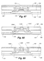
- FIGS. 67-69 A method of metalizing the source/drain regions 118A and 118B as well as the gate 114A is shown in FIGS. 67-69.
- a tungsten layer 134 is formed of sufficient thickness to completely fill vias 128, 130, and 132 shown in FIG. 66.
- the tungsten layer 134 is etched away to the surface of the planarized oxide layer 126' to form tungsten plugs 134A, 134B, and 134C.
- Tungsten plugs 134A and 134C provide electrical contact to the source/drain regions, and tungsten plug 134B provides electric contact to gate 114A.
- FIG. a tungsten layer 134 is formed of sufficient thickness to completely fill vias 128, 130, and 132 shown in FIG. 66.
- the tungsten layer 134 is etched away to the surface of the planarized oxide layer 126' to form tungsten plugs 134A, 134B, and 134C.
- a conventional aluminum or other metal layer 136 (not shown) is patterned and etched to form metal regions 136A, 136B, and 136C that are in electrical contact with tungsten plugs 134A, 134B, and 134C, respectively.
- FIGS. 70-77 illustrate an improved fabrication method for forming a second embodiment of a ferroelectric FET including at least two source/drain regions and a ferroelectric gate structure in which a notched ferroelectric dielectric is formed on a substrate, a gate is formed in the notch of the ferroelectric dielectric, and source/drain regions are formed in the substrate.
- ferroelectric FET a portion of a partially-fabricated ferroelectric FET is shown including silicon or other semiconductor substrate 100, N-well or P-well 102, thick field oxide layers 106 and 108, and a ferroelectric layer 112 formed to a thickness of about 200 to 5000 Angstroms.
- Ferroelectric layer 112 can be any ferroelectric material as described in detail above.
- FIG. 71 the result of two etching steps is shown.
- a first etching step etches ferroelectric layer 112 to form the lateral dimension of the ferroelectric dielectric layer used in the gate structure of the ferroelectric FET.
- a second etching step etches the upper surface of the ferroelectric dielectric 112 to form a notch 111.
- the ferroelectric dielectric region 112 underneath the notch 111 is etched to a thickness of about 50 to 2000 Angstroms, depending upon the initial thickness of ferroelectric layer 112.
- a gate layer 133 is formed over the partially formed transistor.
- Gate layer 133 can be polysilicon, platinum, iridium, or any other suitable electrode material.
- Gate layer 133 is deposited to a thickness of about 300 to 5000 Angstroms, sufficient to fill notch 111.
- gate layer 133 is completely etched away to form a gate 133.
- gate 133 fills former notch 111 and is completely surrounded on three sides by the ferroelectric dielectric layer 112. Note also that the active portion of the gate dielectric immediately below gate 133 is completely surrounded and thus protected from hydrogen exposure and corresponding degradation in electrical performance.
- source/drain regions 118A and 118B of appropriate polarity are formed.
- an oxide layer 126 is formed and planarized.
- vias are etched into oxide layer 126.
- Vias 128 and 132 provide access to source/drain regions 118A and 118B, and via 130 provides access to gate 133.
- a tungsten layer 134 (not shown) has been formed and etched to create tungsten plugs 134A, 134B, and 134C, which are in electrical contact with source/drain region 118A, gate 133, and source/drain region 118B, respectively. Also shown in FIG. 77 are etched aluminum or other metal regions 136A, 136B, and 136C that are in electrical contact with tungsten plugs 134A, 134B, and 134C, respectively.
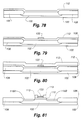
- FIGS. 78-84 illustrate an improved fabrication method for forming a third embodiment of a ferroelectric FET including at least two source/drain regions and a ferroelectric gate structure in which a first ferroelectric layer is formed over the substrate, a gate is formed on the first ferroelectric layer, a second ferroelectric layer is formed over the first ferroelectric layer and gate, the first and second ferroelectric layers are etched to define the lateral dimensions of the dielectric, and the second ferroelectric layer is etched to access the gate.
- ferroelectric layer 112 can be any ferroelectric material as described in detail above.
- a gate layer is etched to form gate 133 as shown sized slightly less than the lateral dimension of the ferroelectric dielectric layer used in the gate structure of the ferroelectric FET.
- the thickness and material for gate 133 is as described in detail above.
- a cap layer 113 is formed over gate 133 and the first ferroelectric layer 112.
- the cap layer 113 can be any doped or undoped ferroelectric material such as PZT, SBT, and BST, or other known ferroelectric materials.
- the cap layer 113 can be a ceramic material selected from a group consisting of doped and undoped nitrides, titanates, zirconates, niobates, tantalates, stanates, hafnates, and manganates, and can be either ferroelectric or non-ferroelectric.
- layers 112 and 113 are etched to define the lateral dimensions of the ferroelectric gate structure, and to surround gate 133 on three sides. Note also that the active portion of ferroelectric dielectric layer 112 is completely surrounded and thus protected from hydrogen degradation. Also shown in FIG. 74 is the formation of the source/drain regions 118A and 118B.
- an oxide layer 126 is formed and planarized.
- vias are etched into oxide layer 126.
- Vias 128 and 132 provide access to source/drain regions 118A and 118B, and via 130 provides access to gate 133.
- a tungsten layer 134 (not shown) has been formed and etched to create tungsten plugs 134A, 134B, and 134C, which are in electrical contact with source/drain region 118A, gate 133, and source/drain region 118B, respectively. Also shown in FIG. 84 are etched aluminum or other metal regions 136A, 136B, and 136C that are in electrical contact with tungsten plugs 134A, 134B, and 134C, respectively.
- FIGS. 85-89 illustrate a method of protecting any ferroelectric device resident on an integrated circuit from hydrogen damage, the method comprising the step of encapsulating the ferroelectric device with a hydrogen-barrier cap layer distinct from the ferroelectric device.
- a ferroelectric device 140 is shown having first and second metal contacts 142 and 144. Although only two contacts are shown, any number can be used.
- Ferroelectric device 140 can be an integrated or bulk capacitor, transistor, sensor, or any other device containing a ferroelectric material that can be damaged in subsequent semiconductor processing steps.
- Cap layer 122 can be formed of a ferroelectric material including doped and undoped PZT, BST, and SBT, or other known ferroelectric materials.
- Cap layer 122 can also be a ferroelectric or non-ferroelectric ceramic material selected from a group consisting of doped and undoped nitrides, titanates, zirconates, niobates, tantalates, stanates, hafnates, and manganates.
- the thickness of layer 122 is determined by the dimensions of ferroelectric device 140 and other processing constraints. While nominal levels can be similar to those described in this disclosure, other thicker layers can be used if desired.
- cap layer 122 is etched to completely encapsulate ferroelectric device 140 and to provide vias 146 and 148 to access metal contacts 142 and 144.
- metal contacts 142 and 144 are metalized with aluminum or other known metalization materials to provide electrical contact to other portions of the integrated circuit.
- an oxide layer or passivation layer 126 is formed and, if desired, planarized.
- the invention can be modified in arrangement and detail without departing from such principles.
- the following aspects of the semiconductor processes described herein can be changed as required: the types of dielectric materials; the thicknesses of the various layers; the types of ferroelectric materials; the etching processes; the electrode materials; and the anneal temperatures, durations, and numbers.
- the specific application of the ferroelectric capacitor of the present invention is not limited to ferroelectric memory cells, although it is ideally suited to that application. We therefore claim all modifications and variation coming within the spirit and scope of the following claims.
Abstract
Description
Claims (35)
- A ferroelectric capacitor comprising:a bottom electrode;a top electrode; anda ferroelectric layer between the top and bottom electrodes extending to completely encapsulate the top electrode, except for a contact hole to allow metalization of the top electrode.
- A ferroelectric capacitor as in claim 1 in which the ferroelectric layer comprises a first layer between the electrodes and a second layer over the top electrode, wherein the thickness of the first layer is approximately the same as the thickness of the second layer.
- A ferroelectric capacitor comprising:a bottom electrode;a ferroelectric layer formed on the bottom electrode, the ferroelectric layer including a partially etched indentation;a top electrode formed in the partially etched indentation; anda dielectric layer formed over the ferroelectric layer including a contact hole to allow metalization of the top electrode.
- A ferroelectric capacitor as in any one of claims 1 to 3 in which the ferroelectric layer comprises PZT.
- A ferroelectric capacitor as in any one of claims 1 to 4 in which the ferroelectric layer comprises SBT.
- A ferroelectric capacitor as in claim 3 in which the dielectric layer comprises an oxide layer.
- A ferroelectric capacitor as in claim 3 in which the dielectric layer comprises a ferroelectric layer.
- A ferroelectric capacitor comprising:
a first electrode, a second electrode, and a ferroelectric layer between the first and second electrodes wherein the first electrode is at least partially encapsulated by ferroelectric material so that at least two faces of the first electrode are covered by ferroelectric material. - A method of fabricating a ferroelectric capacitor comprising the steps of forming a first electrode and a second electrode, and a ferroelectric layer between the first and second electrodes wherein the first electrode is at least partially encapsulated by ferroelectric material so that at least two faces of the first electrode are covered by ferroelectric material.
- The method of claim 9 comprising the steps of forming an unencapsulated ferroelectric capacitor and extending the ferroelectric layer to wholly encapsulate the first electrode by ferroelectric material.
- The fabrication method of claim 10 comprising the steps of:forming an unencapsulated ferroelectric capacitor including a bottom electrode, a top electrode, and a ferroelectric layer between the top and bottom electrodes;extending the ferroelectric layer to completely encapsulate the top electrode such that the opposite state charge relative to the opposite state charge of the unencapsulated ferroelectric capacitor is increased; andforming a contact hole to allow metalization of the top electrode.
- The fabrication method of claim 10 comprising the steps of:forming an unencapsulated ferroelectric capacitor including a bottom electrode, a top electrode, and a ferroelectric layer between the top and bottom electrodes;extending the ferroelectric layer to completely encapsulate the top electrode such that the opposite state charge aging rate relative to the opposite state charge aging rate of the unencapsulated ferroelectric capacitor is decreased; andforming a contact hole to allow metalization of the top electrode.
- The fabrication method of claim 10 comprising the steps of:forming an unencapsulated ferroelectric capacitor including a bottom electrode, a top electrode, and a ferroelectric layer between the top and bottom electrodes;extending the ferroelectric layer to completely encapsulate the top electrode such that the voltage at which the switched charge reaches about 90% of its final value relative to the voltage at which the switched charge reaches about 90% of its final value of the unencapsulated ferroelectric capacitor is decreased; andforming a contact hole to allow metalization of the top electrode.
- The fabrication method of claim 10 comprising the steps of:forming an unencapsulated ferroelectric capacitor including a bottom electrode, a top electrode, and a ferroelectric layer between the top and bottom electrodes;extending the ferroelectric layer to completely encapsulate the top electrode such that the switched charge relative to the switched charge of the unencapsulated ferroelectric capacitor is increased; andforming a contact hole to allow metalization of the top electrode.
- The fabrication method of claim 10 comprising the steps of:forming an unencapsulated ferroelectric capacitor including a bottom electrode, a top electrode, and a ferroelectric layer between the top and bottom electrodes;extending the ferroelectric layer to completely encapsulate the top electrode such that the fatigued switched charge at a predetermined number of switching cycles relative to the fatigued switched charge for the same number of switching cycles of the unencapsulated ferroelectric capacitor is increased; andforming a contact hole to allow metalization of the top electrode.
- The method of any of claims 11 to 15 in which the step of extending the ferroelectric layer comprises the step of forming an additional ferroelectric layer.
- The method of claim 9 comprising the steps of partially encapsulating the said electrode in the ferroelectric layer between the electrodes and forming a dielectric layer over the partially encapsulated electrode.
- The fabrication method of claim 17 comprising the steps of:forming a partially encapsulated ferroelectric capacitor including a bottom electrode, a top electrode, and a ferroelectric layer between the top and bottom electrodes that also partially surrounds the top electrode such that the opposite state charge relative to the opposite state charge of a similar-sized unencapsulated reference ferroelectric capacitor is increased;forming a dielectric layer over the partially encapsulated top electrode; andforming a contact hole in the dielectric layer to allow metalization of the top electrode.
- The fabrication method of claim 17 comprising the steps of:forming a partially encapsulated ferroelectric capacitor including a bottom electrode, a top electrode, and a ferroelectric layer between the top and bottom electrodes that also partially surrounds the top electrode such that the opposite state charge aging rate relative to the opposite state charge aging rate of a similar-sized unencapsulated reference ferroelectric capacitor is decreased;forming a dielectric layer over the partially encapsulated top electrode; andforming a contact hole in the dielectric layer to allow metalization of the top electrode.
- The fabrication method of claim 17 comprising the steps of:forming a partially encapsulated ferroelectric capacitor including a bottom electrode, a top electrode, and a ferroelectric layer between the top and bottom electrodes that also partially surrounds the top electrode such that the voltage at which the switched charge reaches about 90% of its final value relative to the voltage at which the switched charge reaches about 90% of its final value of a similar-sized unencapsulated reference ferroelectric capacitor is decreased;forming a dielectric layer over the partially encapsulated top electrode; andforming a contact hole in the dielectric layer to allow metalization of the top electrode.
- The fabrication method of claim 17 comprising the steps of:forming a partially encapsulated ferroelectric capacitor including a bottom electrode, a top electrode, and a ferroelectric layer between the top and bottom electrodes that also partially surrounds the top electrode such that the switched charge relative to the switched charge of a similar-sized unencapsulated reference ferroelectric capacitor is increased;forming a dielectric layer over the partially encapsulated top electrode; andforming a contact hole in the dielectric layer to allow metalization of the top electrode.
- The fabrication method of claim 17 comprising the steps of:forming a partially encapsulated ferroelectric capacitor including a bottom electrode, a top electrode, and a ferroelectric layer between the top and bottom electrodes that also partially surrounds the top electrode such that the fatigued switched charge at a predetermined number of switching cycles relative to the fatigued switched charge for the same number of switching cycles of a similar-sized unencapsulated reference ferroelectric capacitor is increased;forming a dielectric layer over the partially encapsulated top electrode; andforming a contact hole in the dielectric layer to allow metalization of the top electrode.
- The method of any of claims 18 to 22 in which the step of forming the partially encapsulated ferroelectric capacitor further comprises the steps of:partially etching the ferroelectric layer to form an indentation; andforming the top electrode in the indentation.
- An integrated circuit ferroelectric memory cell having a bit line, a word line, and a plate line, comprising:a silicon substrate or epitaxial region;a transistor formed in the substrate including first and second diffused regions, a thin gate oxide, and a gate forming the word line;a thick oxide layer formed on the substrate including contact holes to allow metalization of the first and second diffused regions;a ferroelectric capacitor formed on the thick oxide layer, the ferroelectric capacitor including a bottom electrode, a ferroelectric layer, and a top electrode, wherein the ferroelectric layer either partially or completely encapsulates the top electrode and includes a contact hole to allow metalization of the top electrode;a first dielectric layer formed over the thick oxide layer and the ferroelectric capacitor including contact holes to allow metalization of the first and second diffused regions, and the top and bottom electrodes of the ferroelectric capacitor;a first patterned metalization layer for contacting the first diffused region, for forming a local interconnect between the top electrode and the second diffused region, and for metalizing the bottom electrode;a second dielectric layer formed over the first metalization layer including contact holes to allow metalization of the first diffused region and the bottom electrode;a second patterned metalization layer for contacting the first diffused region to form the bit line, and for contacting the bottom electrode to form the plate line; anda passivation layer formed over the second metalization layer.
- An integrated circuit ferroelectric memory cell as in claim 24 in which the first dielectric layer comprises a ferroelectric layer.
- An integrated circuit ferroelectric memory cell as in claim 24 or claim 25 in which the second dielectric layer comprises a ferroelectric layer.
- An integrated circuit ferroelectric memory cell as in any of claims 24 to 26 in which the passivation layer comprises a ferroelectric layer.
- An integrated circuit ferroelectric memory cell as in claim 24 in which the ferroelectric layer comprises a material selected from the group consisting of PZT and SBT.
- An integrated circuit ferroelectric memory cell as in claim 24 in which the ferroelectric layer comprises first and second layers of ferroelectric material.
- An integrated circuit ferroelectric memory cell as in claim 24 in which the ferroelectric layer comprises a first layer comprising a material selected from the group consisting of PZT and SBT, and a second layer comprising a material selected from the group consisting of PZT and SBT.
- A ferroelectric memory cell comprising a capacitor as claimed in any one of claims 1 to 8.
- A fabrication method comprising the steps of:forming a ferroelectric FET including at least two source/drain regions and a ferroelectric gate structure; andencapsulating the ferroelectric gate structure with a hydrogen-barrier cap layer distinct from the ferroelectric gate structure.
- A method of protecting a ferroelectric device resident on an integrated circuit from hydrogen damage, the method comprising the step encapsulating the ferroelectric device with a hydrogen-barrier cap layer distinct from the ferroelectric device.
- A ferroelectric FET including at least two source/drain regions, a ferroelectric gate structure and a hydrogen-barrier cap layer distinct from the ferroelectric gate structure.
- An integrated circuit including a ferroelectric device comprising a hydrogen-barrier cap layer distinct from the ferroelectric device.
Applications Claiming Priority (6)
| Application Number | Priority Date | Filing Date | Title |
|---|---|---|---|
| US828157 | 1986-02-10 | ||
| US700076 | 1996-08-20 | ||
| US08/700,076 US5920453A (en) | 1996-08-20 | 1996-08-20 | Completely encapsulated top electrode of a ferroelectric capacitor |
| US728740 | 1996-10-11 | ||
| US08/728,740 US5864932A (en) | 1996-08-20 | 1996-10-11 | Partially or completely encapsulated top electrode of a ferroelectric capacitor |
| US08/828,157 US6027947A (en) | 1996-08-20 | 1997-03-27 | Partially or completely encapsulated top electrode of a ferroelectric capacitor |
Publications (2)
| Publication Number | Publication Date |
|---|---|
| EP0837504A2 true EP0837504A2 (en) | 1998-04-22 |
| EP0837504A3 EP0837504A3 (en) | 1999-01-07 |
Family
ID=27418701
Family Applications (1)
| Application Number | Title | Priority Date | Filing Date |
|---|---|---|---|
| EP97306287A Withdrawn EP0837504A3 (en) | 1996-08-20 | 1997-08-19 | Partially or completely encapsulated ferroelectric device |
Country Status (3)
| Country | Link |
|---|---|
| US (2) | US6211542B1 (en) |
| EP (1) | EP0837504A3 (en) |
| JP (1) | JP4511642B2 (en) |
Cited By (17)
| Publication number | Priority date | Publication date | Assignee | Title |
|---|---|---|---|---|
| EP0996160A1 (en) * | 1998-10-12 | 2000-04-26 | STMicroelectronics S.r.l. | Contact structure for a semiconductor device |
| WO2000031779A1 (en) * | 1998-11-25 | 2000-06-02 | Microchip Technology Incorporated | An improved high quality factor capacitor |
| EP1006582A2 (en) * | 1998-12-03 | 2000-06-07 | Matsushita Electronics Corporation | Semiconductor memory device having a hydrogen barrier, and method for manufacturing the same |
| EP1089339A2 (en) * | 1999-09-28 | 2001-04-04 | Rohm Co., Ltd. | Ferroelectric capacitor and ferrroelectric memory |
| WO2001024237A1 (en) * | 1999-09-28 | 2001-04-05 | Symetrix Corporation | Integrated circuits with barrier layers and methods of fabricating same |
| KR20010109610A (en) * | 2000-05-31 | 2001-12-12 | 박종섭 | A method for forming ferroelectric capacitor in semiconductor device |
| EP1168457A2 (en) * | 2000-06-26 | 2002-01-02 | Ramtron International Corporation | Ferroelectric memory cell and method of manufacture |
| EP1213745A1 (en) * | 2000-12-05 | 2002-06-12 | Sony International (Europe) GmbH | Method of producing a ferroelectric memory and memory device |
| US6579727B1 (en) | 1999-11-10 | 2003-06-17 | Stmicroelectronics S.R.L. | Process for selectively sealing ferroelectric capacitive elements incorporated in semiconductor integrated non-volatile memory cells |
| US6633060B2 (en) | 2000-11-17 | 2003-10-14 | Stmicroelectronics S.R.L. | Contact structure for a ferroelectric memory device |
| EP1386333A1 (en) * | 2001-05-10 | 2004-02-04 | MicroCoating Technologies, Inc. | Capacitor having improved electrodes |
| US6734565B2 (en) | 2001-04-19 | 2004-05-11 | Stmicroelectronics S.R.L. | Contact structure for an integrated semiconductor device |
| US6838718B2 (en) | 1999-09-28 | 2005-01-04 | Rohm Co., Ltd. | Ferroelectric capacitor and ferroelectric memory |
| WO2005064681A2 (en) * | 2003-12-22 | 2005-07-14 | Koninklijke Philips Electronics N.V. | Non-volatile ferroelectric memory device and manufacturing method |
| CN101436465B (en) * | 2007-11-14 | 2013-09-11 | 财团法人工业技术研究院 | Capacitor structure capable of hoisting resonance frequency |
| EP3480833A1 (en) * | 2017-10-23 | 2019-05-08 | BlackBerry Limited | Small-gap coplanar tunable capacitors and methods for manufacturing thereof |
| US10825612B2 (en) | 2017-10-23 | 2020-11-03 | Nxp Usa, Inc. | Tunable coplanar capacitor with vertical tuning and lateral RF path and methods for manufacturing thereof |
Families Citing this family (46)
| Publication number | Priority date | Publication date | Assignee | Title |
|---|---|---|---|---|
| EP0893832A3 (en) * | 1997-07-24 | 1999-11-03 | Matsushita Electronics Corporation | Semiconductor device including a capacitor device and method for fabricating the same |
| KR100279297B1 (en) * | 1998-06-20 | 2001-02-01 | 윤종용 | Semiconductor device and manufacturing method thereof |
| US6509601B1 (en) * | 1998-07-31 | 2003-01-21 | Samsung Electronics Co., Ltd. | Semiconductor memory device having capacitor protection layer and method for manufacturing the same |
| US6174735B1 (en) * | 1998-10-23 | 2001-01-16 | Ramtron International Corporation | Method of manufacturing ferroelectric memory device useful for preventing hydrogen line degradation |
| JP3762148B2 (en) * | 1999-06-30 | 2006-04-05 | 株式会社東芝 | Manufacturing method of semiconductor device |
| KR100360592B1 (en) * | 1999-12-08 | 2002-11-13 | 동부전자 주식회사 | Semiconductor devic and method for fabricating it |
| JP3839239B2 (en) | 2000-10-05 | 2006-11-01 | 株式会社ルネサステクノロジ | Semiconductor integrated circuit device |
| JP2004523924A (en) * | 2001-03-21 | 2004-08-05 | コーニンクレッカ フィリップス エレクトロニクス エヌ ヴィ | Electronic device |
| US7154440B2 (en) * | 2001-04-11 | 2006-12-26 | Kyocera Wireless Corp. | Phase array antenna using a constant-gain phase shifter |
| US6690251B2 (en) * | 2001-04-11 | 2004-02-10 | Kyocera Wireless Corporation | Tunable ferro-electric filter |
| US6937195B2 (en) * | 2001-04-11 | 2005-08-30 | Kyocera Wireless Corp. | Inverted-F ferroelectric antenna |
| US7221243B2 (en) * | 2001-04-11 | 2007-05-22 | Kyocera Wireless Corp. | Apparatus and method for combining electrical signals |
| US7746292B2 (en) | 2001-04-11 | 2010-06-29 | Kyocera Wireless Corp. | Reconfigurable radiation desensitivity bracket systems and methods |
| US7174147B2 (en) * | 2001-04-11 | 2007-02-06 | Kyocera Wireless Corp. | Bandpass filter with tunable resonator |
| US6426250B1 (en) * | 2001-05-24 | 2002-07-30 | Taiwan Semiconductor Manufacturing Company | High density stacked MIM capacitor structure |
| US6423592B1 (en) | 2001-06-26 | 2002-07-23 | Ramtron International Corporation | PZT layer as a temporary encapsulation and hard mask for a ferroelectric capacitor |
| JP2003204043A (en) * | 2001-10-24 | 2003-07-18 | Fujitsu Ltd | Semiconductor device and its manufacturing method |
| JP2003152165A (en) * | 2001-11-15 | 2003-05-23 | Fujitsu Ltd | Semiconductor device and manufacturing method thereof |
| US7184727B2 (en) * | 2002-02-12 | 2007-02-27 | Kyocera Wireless Corp. | Full-duplex antenna system and method |
| US7176845B2 (en) * | 2002-02-12 | 2007-02-13 | Kyocera Wireless Corp. | System and method for impedance matching an antenna to sub-bands in a communication band |
| US6573587B1 (en) * | 2002-05-28 | 2003-06-03 | Oki Electric Industry Co., Ltd. | Metal oxide capacitor with hydrogen diffusion blocking covering |
| US6785119B2 (en) * | 2002-11-29 | 2004-08-31 | Infineon Technologies Ag | Ferroelectric capacitor and process for its manufacture |
| DE10260352A1 (en) * | 2002-12-20 | 2004-07-15 | Infineon Technologies Ag | Method of manufacturing a capacitor arrangement and capacitor arrangement |
| US7720443B2 (en) | 2003-06-02 | 2010-05-18 | Kyocera Wireless Corp. | System and method for filtering time division multiple access telephone communications |
| JP2005116756A (en) * | 2003-10-07 | 2005-04-28 | Fujitsu Ltd | Semiconductor device and its manufacturing method |
| US20060080414A1 (en) * | 2004-07-12 | 2006-04-13 | Dedicated Devices, Inc. | System and method for managed installation of a computer network |
| JP4589092B2 (en) * | 2004-12-03 | 2010-12-01 | 富士通セミコンダクター株式会社 | Manufacturing method of semiconductor device |
| US7548762B2 (en) * | 2005-11-30 | 2009-06-16 | Kyocera Corporation | Method for tuning a GPS antenna matching network |
| US20080001292A1 (en) * | 2006-06-28 | 2008-01-03 | Marina Zelner | Hermetic Passivation Layer Structure for Capacitors with Perovskite or Pyrochlore Phase Dielectrics |
| US8361811B2 (en) * | 2006-06-28 | 2013-01-29 | Research In Motion Rf, Inc. | Electronic component with reactive barrier and hermetic passivation layer |
| JP2008171886A (en) * | 2007-01-09 | 2008-07-24 | Rohm Co Ltd | Semiconductor device and manufacturing method thereof |
| EP2325867A1 (en) * | 2009-11-24 | 2011-05-25 | Nxp B.V. | High-dielectric constant capacitor |
| US9846664B2 (en) | 2010-07-09 | 2017-12-19 | Cypress Semiconductor Corporation | RFID interface and interrupt |
| US9092582B2 (en) | 2010-07-09 | 2015-07-28 | Cypress Semiconductor Corporation | Low power, low pin count interface for an RFID transponder |
| US8723654B2 (en) | 2010-07-09 | 2014-05-13 | Cypress Semiconductor Corporation | Interrupt generation and acknowledgment for RFID |
| FR2964497B1 (en) * | 2010-09-03 | 2013-04-19 | Commissariat Energie Atomique | INTEGRATED CAPACITY COMPRISING AN ELECTRIC INSULATION LAYER OF AMORPHOUS PEROVSKITE MATERIAL AND METHOD OF MANUFACTURE |
| US8765569B2 (en) * | 2011-06-14 | 2014-07-01 | Intermolecular, Inc. | Molybdenum oxide top electrode for DRAM capacitors |
| US8518791B2 (en) | 2011-08-12 | 2013-08-27 | Cypress Semiconductor Corporation | Method for fabricating a damascene self-aligned ferroelectric random access memory (F-RAM) with simultaneous formation of sidewall ferroelectric capacitors |
| US8552515B2 (en) | 2011-08-12 | 2013-10-08 | Cypress Semiconductor Corporation | Method for fabricating a damascene self-aligned ferroelectric random access memory (F-RAM) device structure employing reduced processing steps |
| US8518792B2 (en) | 2011-08-12 | 2013-08-27 | Cypress Semiconductor Corporation | Method for fabricating a damascene self-aligned ferroelectric random access memory (F-RAM) having a ferroelectric capacitor aligned with a three dimensional transistor structure |
| US8916434B2 (en) | 2012-05-11 | 2014-12-23 | Cypress Semiconductor Corporation | Enhanced hydrogen barrier encapsulation method for the control of hydrogen induced degradation of ferroelectric capacitors in an F-RAM process |
| CN103219318B (en) * | 2013-04-12 | 2015-07-08 | 中国电子科技集团公司第十三研究所 | High-temperature-resistant MIM capacitor for microwave internal matching transistor and manufacturing method thereof |
| US9572261B2 (en) | 2015-03-25 | 2017-02-14 | Texas Instruments Incorporated | Conductive through-polymer vias for capacitative structures integrated with packaged semiconductor chips |
| CN113990661A (en) * | 2015-12-18 | 2022-01-28 | 凯米特电子公司 | Capacitor using film for packaging material thickness control and manufacturing method |
| WO2018003445A1 (en) * | 2016-06-28 | 2018-01-04 | 株式会社村田製作所 | Capacitor |
| JP6579502B2 (en) | 2017-07-26 | 2019-09-25 | 株式会社村田製作所 | Capacitors |
Citations (4)
| Publication number | Priority date | Publication date | Assignee | Title |
|---|---|---|---|---|
| EP0469934A2 (en) * | 1990-08-03 | 1992-02-05 | Hitachi, Ltd. | Semiconductor memory device and method of operation thereof |
| EP0513894A2 (en) * | 1991-05-08 | 1992-11-19 | Koninklijke Philips Electronics N.V. | Method of manufacturing a semiconductor device comprising a capacitor with a ferroelectric dielectric, and semiconductor device comprising such a capacitor |
| US5375085A (en) * | 1992-09-30 | 1994-12-20 | Texas Instruments Incorporated | Three-dimensional ferroelectric integrated circuit without insulation layer between memory layers |
| EP0642167A2 (en) * | 1993-08-05 | 1995-03-08 | Matsushita Electronics Corporation | Semiconductor device having capacitor and manufacturing method thereof |
Family Cites Families (31)
| Publication number | Priority date | Publication date | Assignee | Title |
|---|---|---|---|---|
| JPH0682783B2 (en) * | 1985-03-29 | 1994-10-19 | 三菱電機株式会社 | Capacity and manufacturing method thereof |
| DE3602887A1 (en) * | 1986-01-31 | 1987-08-06 | Bayer Ag | NON-VOLATILE ELECTRONIC MEMORY |
| US5192704A (en) * | 1989-06-30 | 1993-03-09 | Texas Instruments Incorporated | Method and apparatus for a filament channel pass gate ferroelectric capacitor memory cell |
| DE4041271C2 (en) * | 1989-12-25 | 1998-10-08 | Toshiba Kawasaki Kk | Semiconductor device with a ferroelectric capacitor |
| JPH03227069A (en) * | 1990-01-31 | 1991-10-08 | Matsushita Electron Corp | Manufacture of semiconductor memory device |
| US5031144A (en) * | 1990-02-28 | 1991-07-09 | Hughes Aircraft Company | Ferroelectric memory with non-destructive readout including grid electrode between top and bottom electrodes |
| NL9000602A (en) * | 1990-03-16 | 1991-10-16 | Philips Nv | METHOD FOR MANUFACTURING A SEMICONDUCTOR DEVICE WITH MEMORY ELEMENTS FORMING CAPACITORS WITH A FERROELECTRIC DIELECTRIC. |
| DE69132627T2 (en) * | 1990-09-28 | 2001-10-11 | Ramtron Int Corp | SEMICONDUCTOR COMPONENT |
| US5119154A (en) * | 1990-12-03 | 1992-06-02 | Micron Technology, Inc. | Ferroelectric capacitor and method for forming local interconnect |
| US5273927A (en) * | 1990-12-03 | 1993-12-28 | Micron Technology, Inc. | Method of making a ferroelectric capacitor and forming local interconnect |
| JP2723386B2 (en) * | 1991-07-02 | 1998-03-09 | シャープ株式会社 | Non-volatile random access memory |
| JPH0563205A (en) * | 1991-09-03 | 1993-03-12 | Sharp Corp | Semiconductor device |
| US5206788A (en) * | 1991-12-12 | 1993-04-27 | Ramtron Corporation | Series ferroelectric capacitor structure for monolithic integrated circuits and method |
| JPH05175460A (en) * | 1991-12-26 | 1993-07-13 | Sharp Corp | Semiconductor memory |
| US5382817A (en) * | 1992-02-20 | 1995-01-17 | Mitsubishi Denki Kabushiki Kaisha | Semiconductor device having a ferroelectric capacitor with a planarized lower electrode |
| JPH05259386A (en) * | 1992-03-11 | 1993-10-08 | Matsushita Electron Corp | Manufacture of ferroelectric thin film |
| US5271955A (en) * | 1992-04-06 | 1993-12-21 | Motorola, Inc. | Method for making a semiconductor device having an anhydrous ferroelectric thin film |
| JP2877618B2 (en) | 1992-07-06 | 1999-03-31 | シャープ株式会社 | Method of forming ferroelectric film |
| US5350705A (en) * | 1992-08-25 | 1994-09-27 | National Semiconductor Corporation | Ferroelectric memory cell arrangement having a split capacitor plate structure |
| JP3161836B2 (en) * | 1992-10-19 | 2001-04-25 | シャープ株式会社 | Semiconductor storage device |
| JP3222243B2 (en) * | 1993-01-25 | 2001-10-22 | 株式会社日立製作所 | Semiconductor storage device and information processing system using the same |
| US5390143A (en) * | 1993-05-17 | 1995-02-14 | Micron Semiconductor, Inc. | Non-volatile static memory devices and operational methods |
| US5479316A (en) * | 1993-08-24 | 1995-12-26 | Analog Devices, Inc. | Integrated circuit metal-oxide-metal capacitor and method of making same |
| US5440173A (en) * | 1993-09-17 | 1995-08-08 | Radiant Technologies | High-temperature electrical contact for making contact to ceramic materials and improved circuit element using the same |
| JPH07111318A (en) * | 1993-10-12 | 1995-04-25 | Olympus Optical Co Ltd | Ferroelectric substance memory |
| US5438023A (en) * | 1994-03-11 | 1995-08-01 | Ramtron International Corporation | Passivation method and structure for a ferroelectric integrated circuit using hard ceramic materials or the like |
| US5822175A (en) * | 1995-04-13 | 1998-10-13 | Matsushita Electronics Corporation | Encapsulated capacitor structure having a dielectric interlayer |
| US5716875A (en) * | 1996-03-01 | 1998-02-10 | Motorola, Inc. | Method for making a ferroelectric device |
| US6027947A (en) * | 1996-08-20 | 2000-02-22 | Ramtron International Corporation | Partially or completely encapsulated top electrode of a ferroelectric capacitor |
| JP3424900B2 (en) * | 1997-10-24 | 2003-07-07 | 松下電器産業株式会社 | Semiconductor device and manufacturing method thereof |
| JP2000243923A (en) * | 1999-02-24 | 2000-09-08 | Asahi Chem Ind Co Ltd | Ferroelectric element |
-
1997
- 1997-08-19 EP EP97306287A patent/EP0837504A3/en not_active Withdrawn
- 1997-08-20 JP JP22407597A patent/JP4511642B2/en not_active Expired - Fee Related
-
1998
- 1998-05-27 US US09/085,280 patent/US6211542B1/en not_active Expired - Lifetime
-
2001
- 2001-01-11 US US09/759,128 patent/US6281023B2/en not_active Expired - Fee Related
Patent Citations (4)
| Publication number | Priority date | Publication date | Assignee | Title |
|---|---|---|---|---|
| EP0469934A2 (en) * | 1990-08-03 | 1992-02-05 | Hitachi, Ltd. | Semiconductor memory device and method of operation thereof |
| EP0513894A2 (en) * | 1991-05-08 | 1992-11-19 | Koninklijke Philips Electronics N.V. | Method of manufacturing a semiconductor device comprising a capacitor with a ferroelectric dielectric, and semiconductor device comprising such a capacitor |
| US5375085A (en) * | 1992-09-30 | 1994-12-20 | Texas Instruments Incorporated | Three-dimensional ferroelectric integrated circuit without insulation layer between memory layers |
| EP0642167A2 (en) * | 1993-08-05 | 1995-03-08 | Matsushita Electronics Corporation | Semiconductor device having capacitor and manufacturing method thereof |
Cited By (33)
| Publication number | Priority date | Publication date | Assignee | Title |
|---|---|---|---|---|
| EP0996160A1 (en) * | 1998-10-12 | 2000-04-26 | STMicroelectronics S.r.l. | Contact structure for a semiconductor device |
| US6541808B2 (en) | 1998-10-12 | 2003-04-01 | Raffaele Zambrano | Contact structure for semiconductor devices and corresponding manufacturing process |
| US6737284B2 (en) | 1998-10-12 | 2004-05-18 | Stmicroelectronics S.R.L. | Contact structure for semiconductor devices and corresponding manufacturing process |
| WO2000031779A1 (en) * | 1998-11-25 | 2000-06-02 | Microchip Technology Incorporated | An improved high quality factor capacitor |
| US6528365B2 (en) | 1998-12-03 | 2003-03-04 | Matsushita Electric Industrial Co., Ltd. | Semiconductor memory device and method for manufacturing the same |
| EP1006582A2 (en) * | 1998-12-03 | 2000-06-07 | Matsushita Electronics Corporation | Semiconductor memory device having a hydrogen barrier, and method for manufacturing the same |
| EP1006580A2 (en) * | 1998-12-03 | 2000-06-07 | Matsushita Electronics Corporation | Semiconductor memory device having a hydrogen barrier layer, and method for manufacturing the same |
| EP1006582A3 (en) * | 1998-12-03 | 2001-06-20 | Matsushita Electronics Corporation | Semiconductor memory device having a hydrogen barrier, and method for manufacturing the same |
| EP1006580A3 (en) * | 1998-12-03 | 2001-06-20 | Matsushita Electronics Corporation | Semiconductor memory device having a hydrogen barrier layer, and method for manufacturing the same |
| US6326671B1 (en) | 1998-12-03 | 2001-12-04 | Matsushita Electronics Corporation | Semiconductor memory device and method for manufacturing the same |
| EP1089339A3 (en) * | 1999-09-28 | 2001-10-10 | Rohm Co., Ltd. | Ferroelectric capacitor and ferrroelectric memory |
| US6838718B2 (en) | 1999-09-28 | 2005-01-04 | Rohm Co., Ltd. | Ferroelectric capacitor and ferroelectric memory |
| WO2001024237A1 (en) * | 1999-09-28 | 2001-04-05 | Symetrix Corporation | Integrated circuits with barrier layers and methods of fabricating same |
| EP1089339A2 (en) * | 1999-09-28 | 2001-04-04 | Rohm Co., Ltd. | Ferroelectric capacitor and ferrroelectric memory |
| US6579727B1 (en) | 1999-11-10 | 2003-06-17 | Stmicroelectronics S.R.L. | Process for selectively sealing ferroelectric capacitive elements incorporated in semiconductor integrated non-volatile memory cells |
| KR20010109610A (en) * | 2000-05-31 | 2001-12-12 | 박종섭 | A method for forming ferroelectric capacitor in semiconductor device |
| EP1168457A2 (en) * | 2000-06-26 | 2002-01-02 | Ramtron International Corporation | Ferroelectric memory cell and method of manufacture |
| EP1168457A3 (en) * | 2000-06-26 | 2004-05-19 | Ramtron International Corporation | Ferroelectric memory cell and method of manufacture |
| US6633060B2 (en) | 2000-11-17 | 2003-10-14 | Stmicroelectronics S.R.L. | Contact structure for a ferroelectric memory device |
| US6878982B2 (en) | 2000-11-17 | 2005-04-12 | Stmicroelectronics S.R.L. | Method of forming a contact structure and a ferroelectric memory device |
| EP1213745A1 (en) * | 2000-12-05 | 2002-06-12 | Sony International (Europe) GmbH | Method of producing a ferroelectric memory and memory device |
| US6756236B2 (en) | 2000-12-05 | 2004-06-29 | Sony International (Europe) Gmbh | Method of producing a ferroelectric memory and a memory device |
| US7052985B2 (en) | 2001-04-19 | 2006-05-30 | Stmicroelectronics S.R.L. | Contact structure for an integrated semiconductor device |
| US6734565B2 (en) | 2001-04-19 | 2004-05-11 | Stmicroelectronics S.R.L. | Contact structure for an integrated semiconductor device |
| EP1386333A1 (en) * | 2001-05-10 | 2004-02-04 | MicroCoating Technologies, Inc. | Capacitor having improved electrodes |
| EP1386333A4 (en) * | 2001-05-10 | 2007-12-12 | Microcoating Technologies Inc | Capacitor having improved electrodes |
| WO2005064681A2 (en) * | 2003-12-22 | 2005-07-14 | Koninklijke Philips Electronics N.V. | Non-volatile ferroelectric memory device and manufacturing method |
| WO2005064681A3 (en) * | 2003-12-22 | 2007-05-18 | Koninkl Philips Electronics Nv | Non-volatile ferroelectric memory device and manufacturing method |
| CN101436465B (en) * | 2007-11-14 | 2013-09-11 | 财团法人工业技术研究院 | Capacitor structure capable of hoisting resonance frequency |
| EP3480833A1 (en) * | 2017-10-23 | 2019-05-08 | BlackBerry Limited | Small-gap coplanar tunable capacitors and methods for manufacturing thereof |
| US10497774B2 (en) | 2017-10-23 | 2019-12-03 | Blackberry Limited | Small-gap coplanar tunable capacitors and methods for manufacturing thereof |
| US10770540B2 (en) | 2017-10-23 | 2020-09-08 | Nxp Usa, Inc. | Small-gap coplanar tunable capacitors and methods for manufacturing thereof |
| US10825612B2 (en) | 2017-10-23 | 2020-11-03 | Nxp Usa, Inc. | Tunable coplanar capacitor with vertical tuning and lateral RF path and methods for manufacturing thereof |
Also Published As
| Publication number | Publication date |
|---|---|
| EP0837504A3 (en) | 1999-01-07 |
| US20010001488A1 (en) | 2001-05-24 |
| US6211542B1 (en) | 2001-04-03 |
| JP4511642B2 (en) | 2010-07-28 |
| JPH10163437A (en) | 1998-06-19 |
| US6281023B2 (en) | 2001-08-28 |
Similar Documents
| Publication | Publication Date | Title |
|---|---|---|
| US6027947A (en) | Partially or completely encapsulated top electrode of a ferroelectric capacitor | |
| EP0837504A2 (en) | Partially or completely encapsulated ferroelectric device | |
| US5864932A (en) | Partially or completely encapsulated top electrode of a ferroelectric capacitor | |
| US6188098B1 (en) | Semiconductor device and method of manufacturing the same | |
| KR100522211B1 (en) | Semiconductor device and method of fabricating the same | |
| US6376325B1 (en) | Method for fabricating a ferroelectric device | |
| US6078492A (en) | Structure of a capacitor in a semiconductor device having a self align contact window which has a slanted sidewall | |
| US6750492B2 (en) | Semiconductor memory with hydrogen barrier | |
| JP3021800B2 (en) | Semiconductor device and manufacturing method thereof | |
| EP0911871A2 (en) | Semiconductor memory device with ferroelectric thin film | |
| US6399974B1 (en) | Semiconductor memory device using an insulator film for the capacitor of the memory cell and method for manufacturing the same | |
| US5920453A (en) | Completely encapsulated top electrode of a ferroelectric capacitor | |
| JP3250257B2 (en) | Semiconductor device and manufacturing method thereof | |
| US6531325B1 (en) | Memory transistor and method of fabricating same | |
| EP0396221B1 (en) | Integrated ferroelectric capacitor | |
| JPH09293869A (en) | Semiconductor device and manufacture thereof | |
| JP2002151657A (en) | Dielectric element and manufacturing method therefor | |
| JP4280006B2 (en) | Semiconductor device | |
| JP3643091B2 (en) | Semiconductor memory device and manufacturing method thereof | |
| KR20070029542A (en) | Manufacturing method of semiconductor memory | |
| US6573553B2 (en) | Semiconductor device and method for fabricating the same | |
| EP0495991A1 (en) | Semiconductor device | |
| US7091538B2 (en) | Semiconductor device and method for manufacturing the same | |
| KR0155866B1 (en) | Ferroelectric memory device and its manufacturing method | |
| JP3111940B2 (en) | Capacity and manufacturing method thereof |
Legal Events
| Date | Code | Title | Description |
|---|---|---|---|
| PUAI | Public reference made under article 153(3) epc to a published international application that has entered the european phase |
Free format text: ORIGINAL CODE: 0009012 |
|
| AK | Designated contracting states |
Kind code of ref document: A2 Designated state(s): DE FR GB IT NL |
|
| AX | Request for extension of the european patent |
Free format text: AL;LT;LV;RO;SI |
|
| PUAL | Search report despatched |
Free format text: ORIGINAL CODE: 0009013 |
|
| AK | Designated contracting states |
Kind code of ref document: A3 Designated state(s): AT BE CH DE DK ES FI FR GB GR IE IT LI LU MC NL PT SE |
|
| AX | Request for extension of the european patent |
Free format text: AL;LT;LV;RO;SI |
|
| RHK1 | Main classification (correction) |
Ipc: H01L 29/92 |
|
| 111Z | Information provided on other rights and legal means of execution |
Free format text: 19990412 AT BE CH DE DK ES FI FR GB GR IE IT LI LU MC NL PT SE |
|
| 17P | Request for examination filed |
Effective date: 19990705 |
|
| AKX | Designation fees paid |
Free format text: DE FR GB IT NL |
|
| STAA | Information on the status of an ep patent application or granted ep patent |
Free format text: STATUS: THE APPLICATION HAS BEEN WITHDRAWN |
|
| 18W | Application withdrawn |
Withdrawal date: 20021031 |