EP0836225A1 - Substrate transfer apparatus and heat treatment system using the same - Google Patents
Substrate transfer apparatus and heat treatment system using the same Download PDFInfo
- Publication number
- EP0836225A1 EP0836225A1 EP96919988A EP96919988A EP0836225A1 EP 0836225 A1 EP0836225 A1 EP 0836225A1 EP 96919988 A EP96919988 A EP 96919988A EP 96919988 A EP96919988 A EP 96919988A EP 0836225 A1 EP0836225 A1 EP 0836225A1
- Authority
- EP
- European Patent Office
- Prior art keywords
- substrate
- transfer apparatus
- transfer
- main body
- heat treatment
- Prior art date
- Legal status (The legal status is an assumption and is not a legal conclusion. Google has not performed a legal analysis and makes no representation as to the accuracy of the status listed.)
- Withdrawn
Links
Images


Classifications
-
- H—ELECTRICITY
- H01—ELECTRIC ELEMENTS
- H01L—SEMICONDUCTOR DEVICES NOT COVERED BY CLASS H10
- H01L21/00—Processes or apparatus adapted for the manufacture or treatment of semiconductor or solid state devices or of parts thereof
- H01L21/67—Apparatus specially adapted for handling semiconductor or electric solid state devices during manufacture or treatment thereof; Apparatus specially adapted for handling wafers during manufacture or treatment of semiconductor or electric solid state devices or components ; Apparatus not specifically provided for elsewhere
- H01L21/68—Apparatus specially adapted for handling semiconductor or electric solid state devices during manufacture or treatment thereof; Apparatus specially adapted for handling wafers during manufacture or treatment of semiconductor or electric solid state devices or components ; Apparatus not specifically provided for elsewhere for positioning, orientation or alignment
-
- H—ELECTRICITY
- H01—ELECTRIC ELEMENTS
- H01L—SEMICONDUCTOR DEVICES NOT COVERED BY CLASS H10
- H01L21/00—Processes or apparatus adapted for the manufacture or treatment of semiconductor or solid state devices or of parts thereof
- H01L21/67—Apparatus specially adapted for handling semiconductor or electric solid state devices during manufacture or treatment thereof; Apparatus specially adapted for handling wafers during manufacture or treatment of semiconductor or electric solid state devices or components ; Apparatus not specifically provided for elsewhere
- H01L21/677—Apparatus specially adapted for handling semiconductor or electric solid state devices during manufacture or treatment thereof; Apparatus specially adapted for handling wafers during manufacture or treatment of semiconductor or electric solid state devices or components ; Apparatus not specifically provided for elsewhere for conveying, e.g. between different workstations
- H01L21/67763—Apparatus specially adapted for handling semiconductor or electric solid state devices during manufacture or treatment thereof; Apparatus specially adapted for handling wafers during manufacture or treatment of semiconductor or electric solid state devices or components ; Apparatus not specifically provided for elsewhere for conveying, e.g. between different workstations the wafers being stored in a carrier, involving loading and unloading
- H01L21/67778—Apparatus specially adapted for handling semiconductor or electric solid state devices during manufacture or treatment thereof; Apparatus specially adapted for handling wafers during manufacture or treatment of semiconductor or electric solid state devices or components ; Apparatus not specifically provided for elsewhere for conveying, e.g. between different workstations the wafers being stored in a carrier, involving loading and unloading involving loading and unloading of wafers
-
- H—ELECTRICITY
- H01—ELECTRIC ELEMENTS
- H01L—SEMICONDUCTOR DEVICES NOT COVERED BY CLASS H10
- H01L21/00—Processes or apparatus adapted for the manufacture or treatment of semiconductor or solid state devices or of parts thereof
- H01L21/02—Manufacture or treatment of semiconductor devices or of parts thereof
- H01L21/04—Manufacture or treatment of semiconductor devices or of parts thereof the devices having at least one potential-jump barrier or surface barrier, e.g. PN junction, depletion layer or carrier concentration layer
- H01L21/18—Manufacture or treatment of semiconductor devices or of parts thereof the devices having at least one potential-jump barrier or surface barrier, e.g. PN junction, depletion layer or carrier concentration layer the devices having semiconductor bodies comprising elements of Group IV of the Periodic System or AIIIBV compounds with or without impurities, e.g. doping materials
- H01L21/30—Treatment of semiconductor bodies using processes or apparatus not provided for in groups H01L21/20 - H01L21/26
- H01L21/324—Thermal treatment for modifying the properties of semiconductor bodies, e.g. annealing, sintering
-
- H—ELECTRICITY
- H01—ELECTRIC ELEMENTS
- H01L—SEMICONDUCTOR DEVICES NOT COVERED BY CLASS H10
- H01L21/00—Processes or apparatus adapted for the manufacture or treatment of semiconductor or solid state devices or of parts thereof
- H01L21/67—Apparatus specially adapted for handling semiconductor or electric solid state devices during manufacture or treatment thereof; Apparatus specially adapted for handling wafers during manufacture or treatment of semiconductor or electric solid state devices or components ; Apparatus not specifically provided for elsewhere
- H01L21/683—Apparatus specially adapted for handling semiconductor or electric solid state devices during manufacture or treatment thereof; Apparatus specially adapted for handling wafers during manufacture or treatment of semiconductor or electric solid state devices or components ; Apparatus not specifically provided for elsewhere for supporting or gripping
- H01L21/687—Apparatus specially adapted for handling semiconductor or electric solid state devices during manufacture or treatment thereof; Apparatus specially adapted for handling wafers during manufacture or treatment of semiconductor or electric solid state devices or components ; Apparatus not specifically provided for elsewhere for supporting or gripping using mechanical means, e.g. chucks, clamps or pinches
- H01L21/68707—Apparatus specially adapted for handling semiconductor or electric solid state devices during manufacture or treatment thereof; Apparatus specially adapted for handling wafers during manufacture or treatment of semiconductor or electric solid state devices or components ; Apparatus not specifically provided for elsewhere for supporting or gripping using mechanical means, e.g. chucks, clamps or pinches the wafers being placed on a robot blade, or gripped by a gripper for conveyance
Definitions
- the present invention relates to a substrate transfer apparatus for transferring a substrate, e.g., a semiconductor wafer, and a heat treatment system using the same.
- a semiconductor manufacturing process has a step of heat-treating a semiconductor wafer as a substrate.
- a heat treatment apparatus which batch-treats a large number of wafers is used in order to effectively achieve required heat treatment.
- a wafer boat made of quartz and mounting a large number of wafers thereon is accommodated in a heat treatment chamber, and the wafers are heat-treated in this heat treatment chamber.
- the wafers accommodated in a wafer carrier made of a resin, e.g., Teflon are transferred therefrom onto the wafer boat to be subjected to heat treatment. After predetermined heat treatment is performed, the wafers are transferred from the wafer boat to the wafer carrier.
- This wafer transfer operation is performed by a transfer apparatus arranged between the wafer carrier and the wafer boat.
- the transfer apparatus main body is moved in the vertical direction and the angular direction in accordance with an operation pattern predetermined by the control mechanism so that it is located at a transfer operation position.
- a wafer carrying fork serving as a treatment target carrying member arranged in the apparatus main body is moved in the horizontal back-and-forth direction. The wafers are transferred between the wafer carrier and the wafer boat by these operations.
- the fork of the transfer apparatus must perform wafer placing and extracting operations while maintaining an appropriate positional relationship with the target position of the arranged substrate holding member, e.g., the carrier or wafer boat, or with the wafer to be transferred.
- the position where the wafer carrier or wafer boat is placed, the posture with which the wafer carrier or wafer boat is placed, and the state of the wafer support grooves are not always the same. More specifically, sometimes the wafer carrier or wafer boat is placed in an inclined state, and various types of displacements may occur in the wafer carrier or wafer boat itself.
- thermal deformation can occur in the heat treatment step. Deformation or strain may occur in the wafer boat due to cleaning performed in order to remove contaminants that attach to the wafer boat during heat treatment.
- a wafer boat having a specific displacement in itself may be replaced. In the carrier, deformation tends to occur entirely or partly since the carrier is made of a resin.
- the operation position of the fork of the transfer apparatus controlled in accordance with the basic operation pattern is actually relatively displaced from the wafer to be transferred, and the aimed transfer operation cannot be sufficiently performed accordingly.
- the wafer extracting operation sometimes the target wafer cannot be placed on the fork in the aimed state.
- the wafer placing operation sometimes the wafer cannot be accurately inserted, or cannot be inserted at all, in the support groove of the wafer support member.
- This teaching is an operation of presetting in the apparatus the coordinate values of the respective wafer grooves of the wafer boat and the coordinate values of the wafer support portion of the corresponding carrier.
- the basic operation pattern of the transfer apparatus is adjusted based on this teaching.
- the groove width of the wafer boat is 3 mm
- the thickness of the wafer is 1 mm
- the clearance above and below the wafer is as very small as 1 mm.
- the wafer and the grooves must be absolutely prevented from rubbing with each other. Therefore, high precision of ⁇ 0.1 mm is required in teaching.
- This teaching operation is conventionally performed with the visual observation of the operator, and this operation is repeated several times until data having allowable precision is obtained. Even if, however, a certain precision is obtained through repeated operations, as it is done with visual confirmation, it is substantially impossible to realize the required high precision of ⁇ 0.1 mm described above.
- the teaching operation takes time since it is performed in a trial-and-error manner by actually moving the fork little by little while confirming the state through visual observation, leading to a long down time of the apparatus, which is inefficient. Since the result of teaching largely depends on the skill of the operator in charge of teaching and the like, the reproducibility of teaching is low. Further, the position of the wafer mounted on the wafer boat must be recognized accurately. However, a semiconductor wafer processing apparatus, e.g., a heat treatment apparatus, usually has a very small inner space. In confirming a portion in the apparatus that needs checking, the operator cannot but do so in an uncomfortable position. The working environment is poor.
- auto-teaching which is done without requiring the operator is developed.
- a technique is known with which a position detection hole is formed in the groove of the wafer boat, the position of the hole is detected by an optical sensor to obtain the position of the boat, and Z-direction positioning that requires particularly high precision is performed.
- the boat is generally made of quartz, it is difficult to detect the boat with an optical sensor, so that stable detection cannot be performed. If the light transmittance or reflectance of quartz changes depending on cleaning or the process, or if the boat thermally deforms, auto-teaching cannot cope with this deformation. Furthermore, a large machining cost is required to fabricate such a boat.
- a sensor for detecting the presence/absence of the wafer to be transferred is required from a viewpoint different from that in teaching. More specifically, when the fork of the transfer apparatus is inserted in, e.g., the wafer boat, whether a wafer is present above the fork must be detected.
- the heat treatment apparatus described above processes expensive wafers, and the wafer boat is also expensive. Accordingly, occurrence of accidents must be prevented.
- the fork may abut against the boat to push or pull it down, to rub the wafer against the groove portion of the boat, or to break the wafer or fork. A counter-measure that prevents occurrence of accidents is required.
- the present invention has been made under these situations, and has as its object to provide a substrate transfer apparatus which can perform auto-teaching accurately, has a mechanism for detecting presence/absence of the wafer as a unit necessary for automatically transferring the wafer, can transfer a substrate with a high reliability while confirming whether or not the substrate always maintains an appropriate positional relationship with a substrate support member, e.g., a wafer boat or wafer carrier, and can be fabricated at a low cost.
- a substrate support member e.g., a wafer boat or wafer carrier
- a substrate transfer apparatus for transferring a substrate between a first substrate support member for supporting a plurality of substrates and a second substrate support member, comprising
- a substrate transfer apparatus for transferring a substrate between a first substrate support member for supporting a plurality of substrates and a second substrate support member, comprising
- a heat treatment system comprising
- a heat treatment system comprising
- the non-contact sensors are mounted on the two side portions of the substrate receiving member that transfers the substrate to/from the first or second substrate support member, to be movable back and forth integrally with the substrate receiving member to detect the distance to the substrate and the position of the substrate in the horizontal plane. Since the distance to the substrate and the position of the substrate in the horizontal plane can be detected, the positions of the substrate receiving member and the target substrate relative to each other can be grasped as three-dimensional data, so that auto-teaching can be performed at high precision. Since the distance to the substrate is detected by the sensors, the presence/absence of the substrate and whether or not the positional relationship between the substrate and the receiving member is accurately maintained can be confirmed, so that the substrate can be transferred at high reliability. Since the sensors only need be mounted on the two sides of the fork, fabrication is easy and its cost is low.
- the plurality of substrate receiving members are arranged to be vertically stacked.
- Non-contact sensors are mounted on one side portion of at least one of the plurality of substrate receiving members and on a side portion, opposite to the one side portion, of at least one of remaining substrate receiving members, to be movable back and forth integrally with the substrate receiving members to detect the distance to the substrate and the position of the substrate in the horizontal plane. Since the distance to the substrate and the position of the substrate in the horizontal plane are detected, the positions of the substrate receiving members and the target substrate relative to each other can be grasped as three-dimensional data, and the same effect as that described above can be obtained.
- FIG. 1 is a perspective view showing an example of a heat treatment apparatus to which a substrate transfer apparatus according to the present invention is applied
- FIG. 2 is a perspective view for explaining movement of a semiconductor wafer in this heat treatment apparatus.
- This heat treatment system 10 basically comprises a heat treatment chamber 27 for heat-treating wafers, a boat elevator 23 for loading/unloading a wafer boat 21 having wafers thereon into/from the heat treatment chamber 27, a carrier stocker 17 for stocking carriers C storing the wafers, and a transfer apparatus 20 for transferring the wafers from the carriers C to the wafer boat 21.
- carriers C each storing, e.g., 25 wafers W, are placed on a direction switching mechanism 13 at an inlet/outlet port 12. The direction of the carriers C is switched by the direction switching mechanism 13 by 90°.
- the carriers C are loaded on a transport stage 15 by a carrier transport mechanism 14 or in the carrier stocker 17 by a carrier elevator 16.
- the wafers W in the carriers C on the transport stage 15 are transferred on the wafer boat 21 by the transfer apparatus 20.
- Reference numeral 29 in FIG. 2 denotes an auto-door 29 for opening/closing the inlet/outlet port 12.
- the wafer boat 21 supporting a predetermined number of wafers W thereon is moved upward by the wafer boat elevator 23 and is inserted in the heat treatment chamber 27 through its lower end which is open upon opening a cap 25. Then, the lower end of the chamber 27 is closed with the cap 25, and the wafers W are heat-treated in this heat treatment chamber 27 with heat from a heater 28.
- the wafer boat 21 is moved downward from the heat treatment chamber 27 to the original position, and the wafers W on the wafer boat 21 are transferred on the carriers C on the transport stage 15 by the transfer apparatus 20.
- Support grooves for supporting the large number of wafers W to be stacked through gaps are formed in the wafer boat 21 or carriers C at predetermined pitches to be separate from each other.
- the opening width of the support grooves of the wafer boat 21 is, e.g., 2 mm when 8-inch wafers having a thickness of 0.725 mm are to be supported, and is, e.g., 1.5 mm when 6-inch wafers having a thickness of 0.65 mm are to be supported.
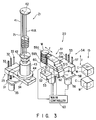
- FIG. 3 is a perspective view showing a state wherein the wafers are transferred from the wafer carrier to the wafer boat and vice versa by using a transfer apparatus according to an embodiment of the present invention.
- the transfer apparatus 20 is located between the carriers C on the transport stage 15 and the wafer boat 21 on the wafer elevator 23.
- the wafer boat elevator 23 has a work table 34 on which the wafer boat 21 is placed, a vertically extending ball screw 32 threadably engaging with the work table 34, a motor 35 for rotating the ball screw 32, vertically extending linear guides 33 for guiding the work table 34, and a support plate 31 for supporting the linear guides 33.
- the ball screw 32 is rotated by the motor 35, the work table 34 is vertically moved along the linear guides 33.
- the wafer boat 21 storing the substrates is loaded into and unloaded from the heat treatment chamber 27.
- the wafer boat 21 is made of a material, e.g., quartz, having excellent heat resistance and corrosion resistance, and has four support columns 41 each having 125 to 180 grooves 41A, a pair of circular plates 42 for fixing the upper and lower end portions of the four support columns 41, a heat-insulating cylinder 43 mounted under the lower circular plate 42, and a flange 44 arranged on the lower end of the heat-insulating cylinder 43.
- a material e.g., quartz, having excellent heat resistance and corrosion resistance
- the flange 44 comes into contact with the flange of the manifold, thereby closing the interior of the heat treatment chamber 27.
- the transfer apparatus 20 has an arm portion 51 for placing the wafers thereon, a support table 52 for supporting the arm portion 51 to be pivotal along a ⁇ direction in a horizontal plane, a motor 53 for pivoting the arm portion 51 along the ⁇ direction, and a drive mechanism 54 for vertically moving the support table 52.
- the drive mechanism 54 has a vertically extending ball screw 55 fixed to the support table 52, a motor 56 for rotating the ball screw 55, vertically extending linear guides 57 for guiding the support table 52, and a support plate 58 for supporting the linear guides 57.
- the support table 52 is vertically moved along the linear guides 58, i.e., in the Z direction.
- the arm portion 51 has an upper portion 51a and a lower portion 51b that are supported on a base portion 60.
- the upper portion 51a and lower portion 51b of the arm portion 51 have five receiving plates 59a and one receiving plate 59b, respectively.
- the five receiving plates 59a can be moved forward/backward at once by a motor 61 in the back-and-forth direction, i.e., in a direction r in Fig. 3.
- the receiving plate 59b can be moved forward/backward by a motor 62 in the direction r .
- These receiving plates 59a and 59b serve as wafer carrying members, and receive and carry the wafers W when they are transferred.
- the motors 61 and 62 are incorporated in the base portion 60.
- This transfer apparatus 20 can receive and deliver the wafers W at a desired position through movement of the support table 52 in the Z direction, movement of the arm portion 51 in the ⁇ direction, and movement of the receiving plates 59a and 59b in the r direction.
- Sensor heads (to be described later) are mounted on the two sides of the receiving plates 59a and 59b. Detection signals from the sensor heads are output to a main controller 63, and control signals are output from the main controller 63 to the respective drive units of the transfer apparatus 20.
- the operation of the transfer apparatus 20 will be described with reference to FIGS. 4 and 5 by way of the operation of extracting the wafers W stored and supported in the carriers C. Although an explanation will be made only regarding the receiving plate 59b for the sake of simplicity, the receiving plates 59a are operated in the same manner. Sensor heads 71a and 71b (to be described later) are mounted on the two sides of the receiving plate 59b.
- the Z-direction position of the support table 52 is adjusted by the drive mechanism 54, and the ⁇ -direction position of the support table 52 is further adjusted by the motor 53, so that the arm portion 51 precisely opposes the carrier C.
- the receiving plate 59b is moved forward to receive the wafer W, and is moved backward.
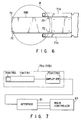
- the structure of the receiving plate 59b will be described in detail with reference to FIGS. 6 and 7.
- the receiving plates 59a are arranged completely in the same manner as the receiving plate 59b.
- FIG. 6 is a plan view of the receiving plate 59b
- FIG. 7 is a view showing the connection state between the receiving plate 59b and a controller.
- the main body of the receiving plate 59b is made of, e.g., alumina or silicon carbide.
- Holding members 72 for holding the wafer W at, e.g., four points, are arranged on the upper surface of the receiving plate 59b.
- the sensor heads 71a and 71b mounted on the two sides of the receiving plate 59b are respectively connected to amplifiers 73a and 73b.
- the sensor heads 71a and 71b, and the amplifiers 73a and 73b constitute electrostatic capacity sensors 70a and 70b serving as non-contact sensors.
- the electrostatic capacity sensors 70a and 70b respectively measure the capacitances between sensor portions 74a and 74b formed at their distal ends, and the wafer W.
- a signal corresponding to the distance is output from the amplifier 73 in accordance with the measured capacitance and input to an interface 81.
- the interface 81 interprets the signal corresponding to the distance output from the amplifier 73 in accordance with the value given in advance or reference supplied from the main controller, and outputs information indicating the presence/absence of the wafer W, information concerning whether or not the wafer W and the receiving plate are maintained at an appropriate distance, and information for auto-teaching to the main controller 63 as ON/OFF signals.
- the main controller 63 outputs a control signal to the drive system of the transfer apparatus 20 based on the input information, thereby controlling the operation of the transfer apparatus 20.
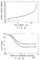
- FIG. 8 is a graph showing a change in sensor output obtained when the sensor head is moved close to the wafer W. Since the detection value is proportional to the inverse of the distance due to the detection principle of the electrostatic capacity sensor, on the near-distance side, the output changes largely even if a change in distance is small. This fact is confirmed from FIG. 8. As a result, high-precision measurement is realized on the near-distance side. From FIG. 8, it is confirmed that high-precision measurement can be performed until the distance between the sensor and wafer is up to 4 mm to 5 mm.
- FIG. 9 is a graph showing a change in sensor output obtained while the receiving plate is driven in the back-and-forth axial direction, after the sensor head is maintained at a position under the wafer to be remote from it by 1.6 mm and 2.1 mm, to extract the sensor head from under the wafer. From FIG. 9, it is known that in both cases the sensor output changes when the sensor head passes by the outer periphery of the wafer. In other words, if a threshold value is set in the sensor, a position of the outer peripheral portion of the wafer is measured as the back-and-forth axial moving amount of the receiving plate.
- the senor that originally measures the distance in the vertical direction can be apparently used to measure a position in the horizontal direction through the emphasizing operation with the drive axis in the horizontal direction.
- the thickness of the sensor head is preferably equal to or smaller than the thickness of the receiving plate so that the sensor head will not abut against other members when moving the receiving plate. Since the thickness of the receiving plate is normally 1.05 mm to 2 mm, the thickness of the sensor head is preferably about 1 mm to 2 mm.
- the main controller 63 processes the information concerning the presence/absence of the wafer W, the information as to whether the wafer W and the receiving plate are at an appropriate distance, and the information for auto-teaching, which are obtained by the interface 81 based on the signals from the electrostatic capacity sensors 70a and 70b, thereby controlling the operation of the transfer apparatus 20.
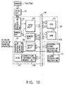
- the main controller 63 has a signal processing unit 91, an input unit 92, a RAM 93, a memory unit 94, a CPU 95, an output unit 96, a transfer apparatus control unit 97, a manual key 105, a correction information memory unit 106, a disk 107, and the like.
- Reference numeral 98 denotes a bus line.
- the main controller 63 is connected to an abnormality signal generating mechanism 100 and an alarm generating mechanism 101 so that an abnormality can be detected.
- a signal from the interface 81 is sent to the input unit 92 as an appropriate signal through the signal processing unit 91, and information from the input unit 92 is loaded in the RAM 93.
- the memory unit 94 stores reference information.
- the CPU 95 compares the detection information and reference information. A command based on this comparison result is output to the transfer apparatus control mechanism 97 through the output unit 96, thereby controlling the operation of the transfer apparatus 20.
- an abnormality signal is output from the abnormality signal generating mechanism 100 to the transfer apparatus control mechanism 97 to stop the operation of the transfer apparatus 20. This signal is also output to the alarm generating mechanism 101 to generate an alarm.
- the main controller 63 loads the signal from the interface 81 again, displays the cause of the abnormality on the display screen (not shown), and waits for the operator's designation.
- the relative positions of the wafer transfer apparatus and target wafer must be fetched as three-dimensional data. More specifically,
- the Z-direction data can be measured directly.
- Data conversion of X- and Y-direction positions are performed in the following manner. If the wafer is offset, the position of the outer periphery detected by the sensor displaces. The offset amount of the wafer is obtained from the displacement amount from the regular position in the opposite manner. More specifically,
- FIG. 11 and FIGS. 12A to 12D show this.
- FIG. 11 shows a method of data conversion of an X-direction position, and indicates a state wherein when one sensor detects the outer peripheral portion of the semiconductor wafer, the other one is offset in the X direction by 18.417 mm.
- the sensor seems to be offset from the semiconductor wafer.
- FIGS. 12A to 12D show a method of data conversion of a Y-direction position, and indicates a change between X-direction data of the two sensors obtained when the respective sensors detect the outer peripheral portion of the semiconductor wafer.
- the differences between X-direction data are 0.609 mm, 1.218 mm, 1.827 mm, and 2.436 mm, respectively. Offset amounts in the Y direction obtained from these differences are 0.5 mm, 1 mm, 1.5 mm, and 2 mm.
- sensors are arranged on the two sides of one mounting receiving plate of the transfer apparatus.
- sensors may be arranged on one side portion of at least one of a plurality of receiving plates and on a side portion, opposite to the one side portion, of at least one of the remaining receiving plates.
- a sensor head 71c can be mounted on only one side portion of the receiving plate 59b described above, and as shown in FIG. 14, a sensor head 71d can be mounted on only a side portion, opposite to the one side portion, of at least one of the receiving plates 59a. This can reduce the number of sensors.
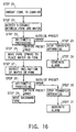
- FIGS. 15A and 15B show the teaching operation at this time.
- a plurality of (n) receiving plates 59a are respectively inserted under the wafers in a safe state (step 1).
- a sensor output is confirmed (step 2). If the obtained value is within a predetermined range, a distance to the wafer is calculated (step 3). If the calculated value does not reach the lower limit of the predetermined range, the receiving plates are moved upward by, e.g., 5 mm (step 4), and step 2 is performed again. This operation is repeated until the calculated value reaches a predetermined value. Then, the receiving plates are moved to a predetermined height, and Z-direction data (Z-data/n) is obtained (step 5).
- n receiving plates 59a are moved to the intermediate point in the back-and-forth axial direction (step 6), and a sensor output obtained at this time is grasped (step 7).
- the position of the outer periphery of the wafer is calculated based on this data, thus obtaining X-direction data (X-data/n) (step 8).
- one receiving plate 59b is inserted under the wafer in a safe state (step 9).
- a sensor output is confirmed (step 10). If the obtained value is within a predetermined range, a distance to the wafer is calculated (step 11). If the calculated value does not reach the lower limit of the predetermined range, the receiving plate is moved upward by, e.g., 5 mm (step 12), and step 10 is performed again. This operation is repeated until the calculated value reaches a predetermined value. Then, the receiving plate is moved to a predetermined height, and Z-direction data (Z-data/1) is obtained (step 13).
- the receiving plate 59b is moved to the intermediate point in the back-and-forth axial direction (step 14), and a sensor output obtained at this time is grasped (step 15).
- the position of the outer periphery of the wafer is calculated based on this data, thus obtaining X-direction data (X-data/1) (step 16).
- Wafer height Z (Z - data/n + Z - data/1)/2
- Wafer position X (X - data/n + X - data/1)/2 + X0
- Wafer position Y (X - data/n - X - data/1)/1.218 + Y0
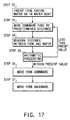
- the arm 51 of the transfer apparatus 20 is moved in the vertical direction (Z direction) in accordance with the basic operation preset in the main controller 63.
- the level of the receiving plate 59b is thus set to match the target wafer W to be transferred which is accommodated in the carrier C.
- the arm 51 is turned in the ⁇ direction so that it precisely opposes the carrier C, i.e., so that the center of the front surface of the carrier C is present on the moving line of the receiving plate 59b in the back-and-forth direction.
- the arm 51 is set at the transfer operation position with respect to the carrier C. From this state, the receiving plate 59b is moved forward and is inserted under the target wafer W (step 21).
- the distance between the receiving plate 59b and wafer W is detected by the sensors 70a and 70b (step 22).
- the main controller 63 performs arithmetic processing based on the detected information and the preset information stored in advance, as described above (step 23).
- the receiving plate 59b is moved slightly upward. Then, the wafer W is took up and carried on the receiving plate (step 24).
- step 25 the transfer apparatus is stopped (step 25), and an alarm is generated (step 26). Appropriate adjustment is performed, and the operation of the apparatus is resumed.
- the inclination of the wafer W is detected by the two sensors 70a and 70b (step 27).
- the main controller 63 performs arithmetic processing based on the inclination information sent from the sensors and the preset information stored in advance (step 28).
- the receiving plate 59b is moved backward, and the target wafer W is extracted from the carrier C (step 29).
- step 30 the transfer apparatus is stopped (step 30), and an alarm is generated (step 31). Appropriate adjustment is performed, and the operation of the apparatus is resumed.
- the target wafer W is extracted from the carrier C, and the wafer is placed on the receiving plate 59b.
- the arm 51 is moved in the vertical direction (Z direction) to set the level of the receiving plate 59b to match the support groove in the wafer boat 21 where the target wafer W must be placed, and the arm 51 is turned to precisely oppose the wafer boat 21.
- the receiving plate 59b is moved forward, and the receiving plate 59b having the wafer W thereon is inserted in the wafer boat 21 (step 32).
- the presence of the wafer on the receiving plate is detected by the sensors 70a and 70b, so that it is confirmed that wafer dropping does not occur and that the transfer operation can be continued.
- the receiving plate 59b is slightly moved downward by a predetermined distance (step 33), and the distance between the receiving plate 59b and wafer W is detected by the sensors 70a and 70b (step 34).
- the main controller 63 performs arithmetic processing based on the detected information and the preset information stored in advance (step 35).
- the receiving plate 59b is moved downward by a predetermined amount. If the detection value is less than a predetermined amount, the receiving plate is moved downward again. This operation is repeated until the amount of downward movement reaches a preset value. The receiving plate is moved downward when the amount of downward movement falls within the preset value range. Therefore, the target wafer W remains on the support groove of the wafer boat 21, so that it is placed in the wafer boat 21 (step S36).
- the receiving plate 59b is moved backward and extracted from the wafer boat 21 (step 37).
- Convey and transfer operations for the next wafer W are performed through the same operation.
- the wafers W are transferred from the carrier C to the wafer boat by repeatedly performing these series of operations.
- Two controllers i.e., the interface 81 and the main controller 63, exist to interpret signals from the sensors, because interpretation of analog data shown in FIG. 8 takes time.
- the main controller interprets the analog data, the operation may be delayed. Therefore, the analog data is converted into ON/OFF signals by the interface 81, and operation is performed in accordance with the ON/OFF signals.
- signal interpretation is controlled by the main controller even if the speed suffers.
- the detailed arrangement of the transfer apparatus according to the present invention is not limited to that of the above embodiment.
- the handling arm and wafer carrying receiving plates those having appropriate shapes and drive mechanisms can be used.
- the wafer support is not limited to what is called a carrier or wafer boat, but various types of wafer supports can be employed.
- the present invention can be similarly applied to a transfer apparatus for transferring plate-like processing targets other than the semiconductor wafer, e.g., LCDs and other substrates.
Abstract
A substrate transfer apparatus (20) transfers a
substrate between a first substrate support member (21)
for supporting a plurality of substrates and a second
substrate support member (15). This apparatus (20)
includes a transfer apparatus main body (60) movable
between a first transfer operation position where it
can perform a substrate transfer operation with respect
to the first substrate support member, and a second
transfer operation position where it can perform a
substrate transfer operation with respect to second
substrate support member, a substrate receiving member
(59b) arranged to be movable back and forth with
respect to the transfer apparatus main body to support
the substrate and to transfer the substrate to/from
the first or second substrate support member, and non-contact
sensors (70a, 70b) mounted on two side portions
of the substrate receiving member (59b) and movable
back and forth integrally with the substrate receiving
member to detect a distance to the substrate and a
position of the substrate in a horizontal plane.
Description
The present invention relates to a substrate
transfer apparatus for transferring a substrate, e.g.,
a semiconductor wafer, and a heat treatment system
using the same.
For example, a semiconductor manufacturing process
has a step of heat-treating a semiconductor wafer as a
substrate. Recently, a heat treatment apparatus which
batch-treats a large number of wafers is used in order
to effectively achieve required heat treatment. In such
a heat treatment apparatus, usually, a wafer boat made
of quartz and mounting a large number of wafers thereon
is accommodated in a heat treatment chamber, and the
wafers are heat-treated in this heat treatment chamber.
Regarding this heat treatment, first, the wafers
accommodated in a wafer carrier made of a resin, e.g.,
Teflon, are transferred therefrom onto the wafer boat
to be subjected to heat treatment. After predetermined
heat treatment is performed, the wafers are transferred
from the wafer boat to the wafer carrier.
This wafer transfer operation is performed by a
transfer apparatus arranged between the wafer carrier
and the wafer boat. In this transfer apparatus, the
transfer apparatus main body is moved in the vertical
direction and the angular direction in accordance with
an operation pattern predetermined by the control
mechanism so that it is located at a transfer operation
position. Also, a wafer carrying fork serving as
a treatment target carrying member arranged in the
apparatus main body is moved in the horizontal back-and-forth
direction. The wafers are transferred
between the wafer carrier and the wafer boat by these
operations.
In the actual transfer operation, the fork of
the transfer apparatus must perform wafer placing and
extracting operations while maintaining an appropriate
positional relationship with the target position of the
arranged substrate holding member, e.g., the carrier or
wafer boat, or with the wafer to be transferred.
The position where the wafer carrier or wafer boat
is placed, the posture with which the wafer carrier
or wafer boat is placed, and the state of the wafer
support grooves are not always the same. More specifically,
sometimes the wafer carrier or wafer boat is
placed in an inclined state, and various types of
displacements may occur in the wafer carrier or wafer
boat itself. For example, in the wafer boat, thermal
deformation can occur in the heat treatment step.
Deformation or strain may occur in the wafer boat due
to cleaning performed in order to remove contaminants
that attach to the wafer boat during heat treatment.
Furthermore, a wafer boat having a specific displacement
in itself may be replaced. In the carrier,
deformation tends to occur entirely or partly since the
carrier is made of a resin.
When various types of these displacements occur
in the wafer support member, or when the wafer support
state of the wafer support member is inappropriate,
the operation position of the fork of the transfer
apparatus controlled in accordance with the basic
operation pattern is actually relatively displaced from
the wafer to be transferred, and the aimed transfer
operation cannot be sufficiently performed accordingly.
For example, in the wafer extracting operation,
sometimes the target wafer cannot be placed on the fork
in the aimed state. In the wafer placing operation,
sometimes the wafer cannot be accurately inserted, or
cannot be inserted at all, in the support groove of the
wafer support member.
From these reasons, when a carrier or wafer boat
is newly arranged, an operation called teaching is
performed so that a transfer operation, which matches
it, is performed.
This teaching is an operation of presetting in the
apparatus the coordinate values of the respective wafer
grooves of the wafer boat and the coordinate values of
the wafer support portion of the corresponding carrier.
The basic operation pattern of the transfer apparatus
is adjusted based on this teaching.
In this case, the groove width of the wafer boat
is 3 mm, the thickness of the wafer is 1 mm, and
accordingly, the clearance above and below the wafer is
as very small as 1 mm. Also, the wafer and the grooves
must be absolutely prevented from rubbing with each
other. Therefore, high precision of ±0.1 mm is
required in teaching.
Since the number of wafers mounted on the wafer
boat is as large as 125 to 180, the number of times
of operations in one teaching is very large. Also,
teaching must be done again every time the boat is
thermally deformed or cleaned by the process, leading
to a high operation frequency.
This teaching operation is conventionally
performed with the visual observation of the operator,
and this operation is repeated several times until
data having allowable precision is obtained. Even if,
however, a certain precision is obtained through
repeated operations, as it is done with visual confirmation,
it is substantially impossible to realize the
required high precision of ±0.1 mm described above.
The teaching operation takes time since it is performed
in a trial-and-error manner by actually moving the fork
little by little while confirming the state through
visual observation, leading to a long down time of the
apparatus, which is inefficient. Since the result of
teaching largely depends on the skill of the operator
in charge of teaching and the like, the reproducibility
of teaching is low. Further, the position of the wafer
mounted on the wafer boat must be recognized accurately.
However, a semiconductor wafer processing apparatus,
e.g., a heat treatment apparatus, usually has a very
small inner space. In confirming a portion in the
apparatus that needs checking, the operator cannot
but do so in an uncomfortable position. The working
environment is poor.
From these reasons, auto-teaching which is done
without requiring the operator is developed. As an
example of auto-teaching, for example, a technique is
known with which a position detection hole is formed in
the groove of the wafer boat, the position of the hole
is detected by an optical sensor to obtain the position
of the boat, and Z-direction positioning that requires
particularly high precision is performed.
However, since the boat is generally made of
quartz, it is difficult to detect the boat with an
optical sensor, so that stable detection cannot be
performed. If the light transmittance or reflectance of
quartz changes depending on cleaning or the process, or
if the boat thermally deforms, auto-teaching cannot
cope with this deformation. Furthermore, a large
machining cost is required to fabricate such a boat.
In the transfer apparatus for automatically
transferring the wafer, a sensor for detecting the
presence/absence of the wafer to be transferred is
required from a viewpoint different from that in
teaching. More specifically, when the fork of the
transfer apparatus is inserted in, e.g., the wafer boat,
whether a wafer is present above the fork must be
detected.
The heat treatment apparatus described above
processes expensive wafers, and the wafer boat is also
expensive. Accordingly, occurrence of accidents must be
prevented. When, however, the distance between the
wafer and the wafer groove of the boat is inappropriate,
the fork may abut against the boat to push or pull it
down, to rub the wafer against the groove portion of
the boat, or to break the wafer or fork. A counter-measure
that prevents occurrence of accidents is
required.
The present invention has been made under these
situations, and has as its object to provide a
substrate transfer apparatus which can perform auto-teaching
accurately, has a mechanism for detecting
presence/absence of the wafer as a unit necessary for
automatically transferring the wafer, can transfer
a substrate with a high reliability while confirming
whether or not the substrate always maintains an
appropriate positional relationship with a substrate
support member, e.g., a wafer boat or wafer carrier,
and can be fabricated at a low cost.
It is another object of the present invention to
provide a heat treatment system using this substrate
transfer apparatus.
According to an aspect of the present invention,
there is provided a substrate transfer apparatus for
transferring a substrate between a first substrate
support member for supporting a plurality of substrates
and a second substrate support member, comprising
According to another aspect of the present
invention, there is provided a substrate transfer
apparatus for transferring a substrate between a first
substrate support member for supporting a plurality
of substrates and a second substrate support member,
comprising
According to still another aspect of the present
invention, there is provided a heat treatment system
comprising
the transfer apparatus comprising
According to still another aspect of the present
invention, there is provided a heat treatment system
comprising
the transfer apparatus comprising
According to one aspect of the present invention,
the non-contact sensors are mounted on the two side
portions of the substrate receiving member that
transfers the substrate to/from the first or second
substrate support member, to be movable back and forth
integrally with the substrate receiving member to
detect the distance to the substrate and the position
of the substrate in the horizontal plane. Since the
distance to the substrate and the position of the
substrate in the horizontal plane can be detected, the
positions of the substrate receiving member and the
target substrate relative to each other can be grasped
as three-dimensional data, so that auto-teaching can be
performed at high precision. Since the distance to the
substrate is detected by the sensors, the presence/absence
of the substrate and whether or not the
positional relationship between the substrate and the
receiving member is accurately maintained can be
confirmed, so that the substrate can be transferred at
high reliability. Since the sensors only need be
mounted on the two sides of the fork, fabrication is
easy and its cost is low.
According to another aspect of the present
invention, the plurality of substrate receiving members
are arranged to be vertically stacked. Non-contact
sensors are mounted on one side portion of at least one
of the plurality of substrate receiving members and on
a side portion, opposite to the one side portion, of
at least one of remaining substrate receiving members,
to be movable back and forth integrally with the
substrate receiving members to detect the distance to
the substrate and the position of the substrate in the
horizontal plane. Since the distance to the substrate
and the position of the substrate in the horizontal
plane are detected, the positions of the substrate
receiving members and the target substrate relative to
each other can be grasped as three-dimensional data,
and the same effect as that described above can be
obtained.
The present invention will be described in detail
with reference to the accompanying drawings. A case
will be described wherein semiconductor wafers are
employed as the substrates and a wafer carrier and
a wafer boat are employed as the substrate support
members.
FIG. 1 is a perspective view showing an example
of a heat treatment apparatus to which a substrate
transfer apparatus according to the present invention
is applied, and FIG. 2 is a perspective view for
explaining movement of a semiconductor wafer in this
heat treatment apparatus.
This heat treatment system 10 basically comprises
a heat treatment chamber 27 for heat-treating wafers,
a boat elevator 23 for loading/unloading a wafer boat
21 having wafers thereon into/from the heat treatment
chamber 27, a carrier stocker 17 for stocking carriers
C storing the wafers, and a transfer apparatus 20 for
transferring the wafers from the carriers C to the
wafer boat 21. In this heat treatment system 10,
carriers C each storing, e.g., 25 wafers W, are placed
on a direction switching mechanism 13 at an inlet/outlet
port 12. The direction of the carriers C is
switched by the direction switching mechanism 13 by 90°.
Subsequently, the carriers C are loaded on a transport
stage 15 by a carrier transport mechanism 14 or in the
carrier stocker 17 by a carrier elevator 16. Thereafter,
the wafers W in the carriers C on the transport stage
15 are transferred on the wafer boat 21 by the transfer
apparatus 20. Reference numeral 29 in FIG. 2 denotes
an auto-door 29 for opening/closing the inlet/outlet
port 12.
The wafer boat 21 supporting a predetermined
number of wafers W thereon is moved upward by the wafer
boat elevator 23 and is inserted in the heat treatment
chamber 27 through its lower end which is open upon
opening a cap 25. Then, the lower end of the chamber 27
is closed with the cap 25, and the wafers W are heat-treated
in this heat treatment chamber 27 with heat
from a heater 28.
When predetermined heat treatment is ended, the
wafer boat 21 is moved downward from the heat treatment
chamber 27 to the original position, and the wafers W
on the wafer boat 21 are transferred on the carriers C
on the transport stage 15 by the transfer apparatus 20.
Support grooves for supporting the large number of
wafers W to be stacked through gaps are formed in the
wafer boat 21 or carriers C at predetermined pitches to
be separate from each other. For example, the opening
width of the support grooves of the wafer boat 21 is,
e.g., 2 mm when 8-inch wafers having a thickness of
0.725 mm are to be supported, and is, e.g., 1.5 mm when
6-inch wafers having a thickness of 0.65 mm are to be
supported.
FIG. 3 is a perspective view showing a state
wherein the wafers are transferred from the wafer
carrier to the wafer boat and vice versa by using
a transfer apparatus according to an embodiment of the
present invention. As shown in FIG. 3, the transfer
apparatus 20 is located between the carriers C on the
transport stage 15 and the wafer boat 21 on the wafer
elevator 23.
The wafer boat elevator 23 has a work table 34
on which the wafer boat 21 is placed, a vertically
extending ball screw 32 threadably engaging with the
work table 34, a motor 35 for rotating the ball screw
32, vertically extending linear guides 33 for guiding
the work table 34, and a support plate 31 for
supporting the linear guides 33. When the ball screw 32
is rotated by the motor 35, the work table 34 is
vertically moved along the linear guides 33. By this
vertical movement, the wafer boat 21 storing the
substrates is loaded into and unloaded from the heat
treatment chamber 27.
The wafer boat 21 is made of a material, e.g.,
quartz, having excellent heat resistance and corrosion
resistance, and has four support columns 41 each having
125 to 180 grooves 41A, a pair of circular plates 42
for fixing the upper and lower end portions of the four
support columns 41, a heat-insulating cylinder 43
mounted under the lower circular plate 42, and a flange
44 arranged on the lower end of the heat-insulating
cylinder 43.
When the wafer boat 21 is loaded in the heat
treatment chamber 27, the flange 44 comes into contact
with the flange of the manifold, thereby closing the
interior of the heat treatment chamber 27.
The transfer apparatus 20 has an arm portion 51
for placing the wafers thereon, a support table 52 for
supporting the arm portion 51 to be pivotal along a
direction in a horizontal plane, a motor 53 for
pivoting the arm portion 51 along the direction, and
a drive mechanism 54 for vertically moving the support
table 52. The drive mechanism 54 has a vertically
extending ball screw 55 fixed to the support table 52,
a motor 56 for rotating the ball screw 55, vertically
extending linear guides 57 for guiding the support
table 52, and a support plate 58 for supporting the
linear guides 57. When the ball screw 55 is rotated by
the motor 56, the support table 52 is vertically moved
along the linear guides 58, i.e., in the Z direction.
The arm portion 51 has an upper portion 51a and a lower
portion 51b that are supported on a base portion 60.
The upper portion 51a and lower portion 51b of the arm
portion 51 have five receiving plates 59a and one
receiving plate 59b, respectively. The five receiving
plates 59a can be moved forward/backward at once by
a motor 61 in the back-and-forth direction, i.e., in
a direction r in Fig. 3. The receiving plate 59b can be
moved forward/backward by a motor 62 in the direction r.
These receiving plates 59a and 59b serve as wafer
carrying members, and receive and carry the wafers W
when they are transferred. The motors 61 and 62 are
incorporated in the base portion 60.
This transfer apparatus 20 can receive and deliver
the wafers W at a desired position through movement of
the support table 52 in the Z direction, movement of
the arm portion 51 in the direction, and movement of
the receiving plates 59a and 59b in the r direction.
Sensor heads (to be described later) are mounted
on the two sides of the receiving plates 59a and 59b.
Detection signals from the sensor heads are output to a
main controller 63, and control signals are output from
the main controller 63 to the respective drive units of
the transfer apparatus 20.
The operation of the transfer apparatus 20 will
be described with reference to FIGS. 4 and 5 by way of
the operation of extracting the wafers W stored and
supported in the carriers C. Although an explanation
will be made only regarding the receiving plate 59b for
the sake of simplicity, the receiving plates 59a are
operated in the same manner. Sensor heads 71a and 71b
(to be described later) are mounted on the two sides of
the receiving plate 59b.
To extract a wafer stored in the carrier C, first,
the Z-direction position of the support table 52 is
adjusted by the drive mechanism 54, and the -direction
position of the support table 52 is further adjusted
by the motor 53, so that the arm portion 51 precisely
opposes the carrier C. Subsequently, the receiving
plate 59b is moved forward to receive the wafer W, and
is moved backward.
The structure of the receiving plate 59b will be
described in detail with reference to FIGS. 6 and 7.
The receiving plates 59a are arranged completely in the
same manner as the receiving plate 59b.
FIG. 6 is a plan view of the receiving plate 59b,
and FIG. 7 is a view showing the connection state
between the receiving plate 59b and a controller. The
main body of the receiving plate 59b is made of, e.g.,
alumina or silicon carbide. Holding members 72 for
holding the wafer W at, e.g., four points, are arranged
on the upper surface of the receiving plate 59b.
The sensor heads 71a and 71b mounted on the two
sides of the receiving plate 59b are respectively
connected to amplifiers 73a and 73b. The sensor heads
71a and 71b, and the amplifiers 73a and 73b constitute
electrostatic capacity sensors 70a and 70b serving as
non-contact sensors.
The electrostatic capacity sensors 70a and 70b
respectively measure the capacitances between sensor
portions 74a and 74b formed at their distal ends, and
the wafer W. A signal corresponding to the distance is
output from the amplifier 73 in accordance with the
measured capacitance and input to an interface 81.
The interface 81 interprets the signal corresponding to
the distance output from the amplifier 73 in accordance
with the value given in advance or reference supplied
from the main controller, and outputs information
indicating the presence/absence of the wafer W,
information concerning whether or not the wafer W and
the receiving plate are maintained at an appropriate
distance, and information for auto-teaching to the main
controller 63 as ON/OFF signals. The main controller 63
outputs a control signal to the drive system of the
transfer apparatus 20 based on the input information,
thereby controlling the operation of the transfer
apparatus 20.
FIG. 8 is a graph showing a change in sensor
output obtained when the sensor head is moved close to
the wafer W. Since the detection value is proportional
to the inverse of the distance due to the detection
principle of the electrostatic capacity sensor, on the
near-distance side, the output changes largely even if
a change in distance is small. This fact is confirmed
from FIG. 8. As a result, high-precision measurement is
realized on the near-distance side. From FIG. 8, it is
confirmed that high-precision measurement can be
performed until the distance between the sensor and
wafer is up to 4 mm to 5 mm.
FIG. 9 is a graph showing a change in sensor
output obtained while the receiving plate is driven in
the back-and-forth axial direction, after the sensor
head is maintained at a position under the wafer to be
remote from it by 1.6 mm and 2.1 mm, to extract the
sensor head from under the wafer. From FIG. 9, it is
known that in both cases the sensor output changes when
the sensor head passes by the outer periphery of the
wafer. In other words, if a threshold value is set in
the sensor, a position of the outer peripheral portion
of the wafer is measured as the back-and-forth axial
moving amount of the receiving plate.
From the above facts, the sensor that originally
measures the distance in the vertical direction can be
apparently used to measure a position in the horizontal
direction through the emphasizing operation with the
drive axis in the horizontal direction.
The thickness of the sensor head is preferably
equal to or smaller than the thickness of the receiving
plate so that the sensor head will not abut against
other members when moving the receiving plate.
Since the thickness of the receiving plate is normally
1.05 mm to 2 mm, the thickness of the sensor head is
preferably about 1 mm to 2 mm.
The main controller 63 processes the information
concerning the presence/absence of the wafer W, the
information as to whether the wafer W and the receiving
plate are at an appropriate distance, and the
information for auto-teaching, which are obtained
by the interface 81 based on the signals from the
electrostatic capacity sensors 70a and 70b, thereby
controlling the operation of the transfer apparatus 20.
As shown in FIG. 10, the main controller 63 has
a signal processing unit 91, an input unit 92, a RAM
93, a memory unit 94, a CPU 95, an output unit 96, a
transfer apparatus control unit 97, a manual key 105,
a correction information memory unit 106, a disk 107,
and the like. Reference numeral 98 denotes a bus line.
The main controller 63 is connected to an abnormality
signal generating mechanism 100 and an alarm generating
mechanism 101 so that an abnormality can be detected.
In this main controller 63, a signal from the
interface 81 is sent to the input unit 92 as an
appropriate signal through the signal processing unit
91, and information from the input unit 92 is loaded
in the RAM 93. The memory unit 94 stores reference
information. The CPU 95 compares the detection
information and reference information. A command based
on this comparison result is output to the transfer
apparatus control mechanism 97 through the output unit
96, thereby controlling the operation of the transfer
apparatus 20.
In an ordinary transfer operation, when a signal
from the interface 81 guarantees the presence/absence
of a wafer and that the wafer maintains an appropriate
position, a transfer operation continues.
When a signal from the interface 81 indicates
an abnormality, that is, when the wafer is not in
a supposed state or the wafer is not located at an
appropriate position, an abnormality signal is output
from the abnormality signal generating mechanism 100 to
the transfer apparatus control mechanism 97 to stop the
operation of the transfer apparatus 20. This signal is
also output to the alarm generating mechanism 101 to
generate an alarm. After the apparatus is stopped, the
main controller 63 loads the signal from the interface
81 again, displays the cause of the abnormality on
the display screen (not shown), and waits for the
operator's designation.
Auto-teaching done by the transfer apparatus 20
will be described.
To realize auto-teaching, the relative positions
of the wafer transfer apparatus and target wafer must
be fetched as three-dimensional data. More specifically,
- Z-direction data:
- vertical direction
- X-direction data:
- back-and-forth axial direction of the receiving plate
- Y-direction data:
- direction
When an electrostatic capacity sensor is used,
the Z-direction data can be measured directly.
Data conversion of X- and Y-direction positions are
performed in the following manner. If the wafer is
offset, the position of the outer periphery detected by
the sensor displaces. The offset amount of the wafer is
obtained from the displacement amount from the regular
position in the opposite manner. More specifically,
FIG. 11 and FIGS. 12A to 12D show this.
FIG. 11 shows a method of data conversion of an
X-direction position, and indicates a state wherein
when one sensor detects the outer peripheral portion of
the semiconductor wafer, the other one is offset in the
X direction by 18.417 mm. In FIG. 11, for the sake of
illustrative convenience, the sensor seems to be offset
from the semiconductor wafer.
FIGS. 12A to 12D show a method of data conversion
of a Y-direction position, and indicates a change
between X-direction data of the two sensors obtained
when the respective sensors detect the outer peripheral
portion of the semiconductor wafer. In FIGS. 12A to 12D,
the differences between X-direction data are 0.609 mm,
1.218 mm, 1.827 mm, and 2.436 mm, respectively. Offset
amounts in the Y direction obtained from these
differences are 0.5 mm, 1 mm, 1.5 mm, and 2 mm.
A case wherein sensors are arranged on the two
sides of one mounting receiving plate of the transfer
apparatus is described above. However, sensors may
be arranged on one side portion of at least one of
a plurality of receiving plates and on a side portion,
opposite to the one side portion, of at least one of
the remaining receiving plates.
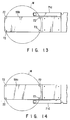
For example, as shown in FIG. 13, a sensor head
71c can be mounted on only one side portion of the
receiving plate 59b described above, and as shown in
FIG. 14, a sensor head 71d can be mounted on only a
side portion, opposite to the one side portion, of at
least one of the receiving plates 59a. This can reduce
the number of sensors.
When auto-teaching is performed by the transfer
apparatus having this arrangement, if the sensor
located at a lower position is moved upward and used,
two types of data can be fetched in the same manner as
in a case wherein sensors are arranged on the two sides.
FIGS. 15A and 15B show the teaching operation at
this time.
First, as shown in FIG. 15A, a plurality of (n)
receiving plates 59a are respectively inserted under
the wafers in a safe state (step 1). A sensor output is
confirmed (step 2). If the obtained value is within a
predetermined range, a distance to the wafer is
calculated (step 3). If the calculated value does not
reach the lower limit of the predetermined range, the
receiving plates are moved upward by, e.g., 5 mm (step
4), and step 2 is performed again. This operation is
repeated until the calculated value reaches a predetermined
value. Then, the receiving plates are moved to
a predetermined height, and Z-direction data (Z-data/n)
is obtained (step 5). Thereafter, the n receiving
plates 59a are moved to the intermediate point in the
back-and-forth axial direction (step 6), and a sensor
output obtained at this time is grasped (step 7).
The position of the outer periphery of the wafer
is calculated based on this data, thus obtaining
X-direction data (X-data/n) (step 8).
Subsequently, as shown in FIG. 15B, one receiving
plate 59b is inserted under the wafer in a safe state
(step 9). A sensor output is confirmed (step 10).
If the obtained value is within a predetermined range,
a distance to the wafer is calculated (step 11). If the
calculated value does not reach the lower limit of the
predetermined range, the receiving plate is moved
upward by, e.g., 5 mm (step 12), and step 10 is
performed again. This operation is repeated until the
calculated value reaches a predetermined value. Then,
the receiving plate is moved to a predetermined height,
and Z-direction data (Z-data/1) is obtained (step 13).
Thereafter, the receiving plate 59b is moved to the
intermediate point in the back-and-forth axial
direction (step 14), and a sensor output obtained at
this time is grasped (step 15). The position of the
outer periphery of the wafer is calculated based on
this data, thus obtaining X-direction data (X-data/1)
(step 16).
Data conversion is performed in the following
manner.
Wafer height Z = (Z - data/n + Z - data/1)/2 Wafer position X = (X - data/n + X - data/1)/2 + X0 Wafer position Y = (X - data/n - X - data/1)/1.218 + Y0
The actual wafer transfer operation done by the
transfer apparatus of the present invention after
teaching is ended will be briefly described with
reference to FIGS. 16 and 17. Although the operation of
the receiving plate 59b will be described, the
receiving plates 59a are operated in the same manner.
First, the arm 51 of the transfer apparatus 20
is moved in the vertical direction (Z direction) in
accordance with the basic operation preset in the main
controller 63. The level of the receiving plate 59b is
thus set to match the target wafer W to be transferred
which is accommodated in the carrier C. Also, the arm
51 is turned in the direction so that it precisely
opposes the carrier C, i.e., so that the center of the
front surface of the carrier C is present on the moving
line of the receiving plate 59b in the back-and-forth
direction. Hence, the arm 51 is set at the transfer
operation position with respect to the carrier C. From
this state, the receiving plate 59b is moved forward
and is inserted under the target wafer W (step 21).
In this state, the distance between the receiving
plate 59b and wafer W is detected by the sensors 70a
and 70b (step 22).
The main controller 63 performs arithmetic
processing based on the detected information and the
preset information stored in advance, as described
above (step 23).
As the result of the arithmetic processing, if the
detection value falls within a preset value range, the
receiving plate 59b is moved slightly upward. Then, the
wafer W is took up and carried on the receiving plate
(step 24).
As the result of the arithmetic processing, if the
detected value falls outside the preset value range,
the transfer apparatus is stopped (step 25), and an
alarm is generated (step 26). Appropriate adjustment is
performed, and the operation of the apparatus is
resumed.
After the distance between the receiving plate 59b
and wafer W is within the preset range and the wafer W
is placed on the receiving plate 59b, the inclination
of the wafer W is detected by the two sensors 70a and
70b (step 27).
The main controller 63 performs arithmetic
processing based on the inclination information sent
from the sensors and the preset information stored in
advance (step 28).
As the result of the arithmetic processing, if the
detection value is within the preset value range, the
receiving plate 59b is moved backward, and the target
wafer W is extracted from the carrier C (step 29).
As the result of the arithmetic processing, if the
detected value falls outside the preset value range,
the transfer apparatus is stopped (step 30), and an
alarm is generated (step 31). Appropriate adjustment is
performed, and the operation of the apparatus is
resumed.
Subsequently, the target wafer W is extracted from
the carrier C, and the wafer is placed on the receiving
plate 59b. Thereafter, the arm 51 is moved in the
vertical direction (Z direction) to set the level of
the receiving plate 59b to match the support groove in
the wafer boat 21 where the target wafer W must be
placed, and the arm 51 is turned to precisely oppose
the wafer boat 21. From this state, the receiving plate
59b is moved forward, and the receiving plate 59b
having the wafer W thereon is inserted in the wafer
boat 21 (step 32). At this time, the presence of the
wafer on the receiving plate is detected by the sensors
70a and 70b, so that it is confirmed that wafer
dropping does not occur and that the transfer operation
can be continued.
Subsequently, the receiving plate 59b is slightly
moved downward by a predetermined distance (step 33),
and the distance between the receiving plate 59b
and wafer W is detected by the sensors 70a and 70b
(step 34).
The main controller 63 performs arithmetic
processing based on the detected information and the
preset information stored in advance (step 35).
As the result of the arithmetic processing, if the
detection value falls within a preset value range, the
receiving plate 59b is moved downward by a predetermined
amount. If the detection value is less than
a predetermined amount, the receiving plate is moved
downward again. This operation is repeated until the
amount of downward movement reaches a preset value. The
receiving plate is moved downward when the amount of
downward movement falls within the preset value range.
Therefore, the target wafer W remains on the support
groove of the wafer boat 21, so that it is placed in
the wafer boat 21 (step S36).
Thereafter, the receiving plate 59b is moved
backward and extracted from the wafer boat 21 (step 37).
Convey and transfer operations for the next wafer
W are performed through the same operation. The wafers
W are transferred from the carrier C to the wafer boat
by repeatedly performing these series of operations.
When setting wafers in the carrier C and wafer boat, it
is usually done sequentially downward. When extracting
the wafers, it is usually done upward.
Two controllers, i.e., the interface 81 and the
main controller 63, exist to interpret signals from the
sensors, because interpretation of analog data shown in
FIG. 8 takes time. During an ordinary operation, if the
main controller interprets the analog data, the
operation may be delayed. Therefore, the analog data is
converted into ON/OFF signals by the interface 81, and
operation is performed in accordance with the ON/OFF
signals. During auto-teaching, signal interpretation is
controlled by the main controller even if the speed
suffers.
The detailed arrangement of the transfer apparatus
according to the present invention is not limited to
that of the above embodiment. For example, regarding
the handling arm and wafer carrying receiving plates,
those having appropriate shapes and drive mechanisms
can be used. The wafer support is not limited to what
is called a carrier or wafer boat, but various types of
wafer supports can be employed.
Further, the present invention can be similarly
applied to a transfer apparatus for transferring plate-like
processing targets other than the semiconductor
wafer, e.g., LCDs and other substrates.
Claims (12)
- A substrate transfer apparatus for transferring a substrate between a first substrate support member for supporting a plurality of substrates and a second substrate support member, comprisinga transfer apparatus main body movable between a first transfer operation position where said transfer apparatus main body can perform a substrate transfer operation with respect to said first substrate support member, and a second transfer operation position where said transfer apparatus main body can perform a substrate transfer operation with respect to said second substrate support member,a substrate receiving member arranged to be movable back and forth with respect to said transfer apparatus main body to support the substrate and to transfer the substrate to/from said first or second substrate support member, andnon-contact sensors mounted on two side portions of said substrate receiving member and movable back and forth integrally with said substrate receiving member to detect a distance to the substrate and a position of the substrate in a horizontal plane.
- A substrate transfer apparatus according to claim 1, further comprising control means for controlling operations of said apparatus main body and said substrate receiving member based on information from said non-contact sensors.
- A substrate transfer apparatus according to claim 1, wherein said non-contact sensors are electrostatic capacity sensors.
- A substrate transfer apparatus for transferring a substrate between a first substrate support member for supporting a plurality of substrates and a second substrate support member, comprisinga transfer apparatus main body movable between a first transfer operation position where said transfer apparatus main body can perform a transfer operation with respect to said first substrate support member, and a second transfer operation position where said transfer apparatus main body can perform a transfer operation with respect to said second substrate support member,a plurality of substrate receiving members arranged to be movable back and forth with respect to said transfer apparatus main body and vertically stacked to support the substrate and transfer the substrate to/from said first or second substrate support member, andat least two non-contact sensors respectively mounted on one side portion of at least one of said plurality of substrate receiving members and on a side portion, opposite to said one side portion, of at least one of remaining substrate receiving members and movable back and forth integrally with corresponding ones of said substrate receiving members to detect a distance to the substrate and a position of the substrate in a horizontal plane.
- A substrate transfer apparatus according to claim 4, further comprising control means for controlling operations of said apparatus main body and said substrate receiving members based on information from said non-contact sensors.
- A substrate transfer apparatus according to claim 4, wherein said non-contact sensors are electrostatic capacity sensors.
- A heat treatment system comprisinga substrate heat treatment section for heat-treating a substrate,a substrate storage section for storing a substrate, anda substrate transfer apparatus for transferring a substrate between said substrate heat treatment section and said substrate storage section,said substrate heat treatment section comprising a heat treatment chamber, a substrate support boat for supporting a large number of substrates, and a loading/unloading mechanism for loading/unloading said substrate support boat into/from said heat treatment chamber,said substrate storage section comprising a storage receptacle for storing a plurality of substrate cassettes for supporting the large number of substrates, and a transport mechanism for transporting a cassette between said storage receptacle and a position corresponding to said transfer apparatus, and
said transfer apparatus comprisinga transfer apparatus main body movable between a first transfer operation position where said transfer apparatus main body can perform a substrate transfer operation with respect to said substrate support boat, and a second transfer operation position where said transfer apparatus main body can perform a substrate transfer operation with respect to said cassettes,a substrate receiving member arranged to be movable back and forth with respect to said transfer apparatus main body to support the substrate and to transfer the substrate to/from said substrate support boat or said cassette, andnon-contact sensors mounted on two side portions of said substrate receiving member and movable back and forth integrally with said substrate receiving member to detect a distance to the substrate and a position of the substrate in a horizontal plane. - A heat treatment system according to claim 7, further comprising control means for controlling operations of said apparatus main body and said substrate receiving member based on information from said non-contact sensors.
- A heat treatment system according to claim 7, wherein said non-contact sensors are electrostatic capacity sensors.
- A heat treatment system comprisinga substrate heat treatment section for heat-treating a substrate,a substrate storage section for storing a substrate, anda substrate transfer apparatus for transferring a substrate between said substrate heat treatment section and said substrate storage section,said substrate heat treatment section comprising a heat treatment chamber, a substrate support boat for supporting a large number of substrates, and a loading/unloading mechanism for loading/unloading said substrate support boat into/from said heat treatment chamber,said substrate storage section comprising a storage receptacle for storing a plurality of substrate cassettes for supporting the large number of substrates, and a transport mechanism for transporting a cassette between said storage receptacle and a position corresponding to said transfer apparatus, and
said transfer apparatus comprisinga transfer apparatus main body movable between a first transfer operation position where said transfer apparatus main body can perform a substrate transfer operation with respect to said substrate support boat, and a second transfer operation position where said transfer apparatus main body can perform a substrate transfer operation with respect to said cassettes,a plurality of substrate receiving members arranged to be movable back and forth with respect to said transfer apparatus main body and vertically stacked to support the substrate and to transfer the substrate to/from said substrate support boat or said cassette, andnon-contact sensors mounted on one side portion of at least one of said plurality of substrate receiving members and on a side portion, opposite to said one side portion, of at least one of remaining substrate receiving members and movable back and forth integrally with corresponding ones of said substrate receiving members to detect a distance to the substrate and a position of the substrate in a horizontal plane. - A heat treatment system according to claim 10, further comprising control means for controlling operations of said apparatus main body and said substrate receiving members based on information from said non-contact sensors.
- A heat treatment system according to claim 10, wherein said non-contact sensors are electrostatic capacity sensors.
Applications Claiming Priority (3)
| Application Number | Priority Date | Filing Date | Title |
|---|---|---|---|
| JP7140653A JPH08335622A (en) | 1995-06-07 | 1995-06-07 | Substrate conveyer |
| JP140653/95 | 1995-06-07 | ||
| PCT/JP1996/001442 WO1996041371A1 (en) | 1995-06-07 | 1996-05-29 | Substrate transfer apparatus and heat treatment system using the same |
Publications (1)
| Publication Number | Publication Date |
|---|---|
| EP0836225A1 true EP0836225A1 (en) | 1998-04-15 |
Family
ID=15273656
Family Applications (1)
| Application Number | Title | Priority Date | Filing Date |
|---|---|---|---|
| EP96919988A Withdrawn EP0836225A1 (en) | 1995-06-07 | 1996-05-29 | Substrate transfer apparatus and heat treatment system using the same |
Country Status (6)
| Country | Link |
|---|---|
| US (1) | US6032083A (en) |
| EP (1) | EP0836225A1 (en) |
| JP (1) | JPH08335622A (en) |
| KR (1) | KR19990021969A (en) |
| TW (1) | TW309502B (en) |
| WO (1) | WO1996041371A1 (en) |
Cited By (2)
| Publication number | Priority date | Publication date | Assignee | Title |
|---|---|---|---|---|
| US8238017B2 (en) | 2009-12-18 | 2012-08-07 | Alcatel Lucent | Photonic match filter |
| US11688617B2 (en) | 2018-12-11 | 2023-06-27 | Rorze Corporation | Electrostatic capacitance sensor |
Families Citing this family (27)
| Publication number | Priority date | Publication date | Assignee | Title |
|---|---|---|---|---|
| TW319751B (en) * | 1995-05-18 | 1997-11-11 | Toshiba Co Ltd | |
| JP3977485B2 (en) * | 1997-04-24 | 2007-09-19 | 東京エレクトロン株式会社 | Arm access position detection method and vacuum processing apparatus |
| US6244121B1 (en) * | 1998-03-06 | 2001-06-12 | Applied Materials, Inc. | Sensor device for non-intrusive diagnosis of a semiconductor processing system |
| US6298280B1 (en) * | 1998-09-28 | 2001-10-02 | Asyst Technologies, Inc. | Method for in-cassette wafer center determination |
| US6405101B1 (en) | 1998-11-17 | 2002-06-11 | Novellus Systems, Inc. | Wafer centering system and method |
| US6238160B1 (en) * | 1998-12-02 | 2001-05-29 | Taiwan Semiconductor Manufacturing Company, Ltd' | Method for transporting and electrostatically chucking a semiconductor wafer or the like |
| US6168066B1 (en) * | 1999-04-21 | 2001-01-02 | Lockheed Martin Corp. | Friction stir conduction controller |
| JP4402811B2 (en) * | 2000-05-26 | 2010-01-20 | 東京エレクトロン株式会社 | SUBSTITUTION CONVEYING SYSTEM AND METHOD FOR DETECTING POSITION SHIFT |
| JP2002062105A (en) * | 2000-08-23 | 2002-02-28 | Sunx Ltd | Head-separated-type sensor, capacitance-type sensor, and wafer detecting device |
| US20040052631A1 (en) * | 2002-09-13 | 2004-03-18 | Chan Kun Yuan | Mechanical arm device for carrying and detecting wafer |
| US7572092B2 (en) | 2002-10-07 | 2009-08-11 | Brooks Automation, Inc. | Substrate alignment system |
| JP4124449B2 (en) * | 2003-03-28 | 2008-07-23 | 大日本スクリーン製造株式会社 | Substrate processing equipment |
| US6944517B2 (en) * | 2003-07-03 | 2005-09-13 | Brooks Automation, Inc. | Substrate apparatus calibration and synchronization procedure |
| JP4255791B2 (en) * | 2003-09-22 | 2009-04-15 | 大日本スクリーン製造株式会社 | Substrate processing equipment |
| KR100568867B1 (en) * | 2004-03-18 | 2006-04-10 | 삼성전자주식회사 | Semiconductor manufacture device sensing coordinates of wafer and device sensing coordinates of wafer therefor |
| US20060245871A1 (en) * | 2005-03-10 | 2006-11-02 | Wen-Ming Lo | Wafer transfer system, wafer transfer method, cassette exchange system and cassette exchange method |
| US8112177B2 (en) | 2005-07-15 | 2012-02-07 | Kabushiki Kaisha Yaskawa Denki | Wafer position teaching method and teaching tool |
| JP4993614B2 (en) * | 2008-02-29 | 2012-08-08 | 東京エレクトロン株式会社 | Teaching method for conveying means, storage medium, and substrate processing apparatus |
| JP5131094B2 (en) | 2008-08-29 | 2013-01-30 | 東京エレクトロン株式会社 | Heat treatment apparatus, heat treatment method, and storage medium |
| JP5635270B2 (en) * | 2009-02-13 | 2014-12-03 | 株式会社日立国際電気 | Substrate processing apparatus, substrate processing system, display method of substrate processing apparatus, parameter setting method of substrate processing apparatus, and recording medium |
| JP6196870B2 (en) * | 2013-10-09 | 2017-09-13 | 株式会社ディスコ | Wafer transfer device |
| US9666465B2 (en) * | 2013-12-12 | 2017-05-30 | Seagate Technology Llc | Positioning apparatus |
| JP6468856B2 (en) * | 2015-01-20 | 2019-02-13 | リンテック株式会社 | Transfer equipment |
| JP7240414B2 (en) * | 2018-12-07 | 2023-03-15 | 川崎重工業株式会社 | Substrate transfer device and its operation method |
| CN110931409A (en) * | 2019-11-26 | 2020-03-27 | 武汉新芯集成电路制造有限公司 | Wafer position identification system and method |
| JP2022064490A (en) | 2020-10-14 | 2022-04-26 | 東京エレクトロン株式会社 | Substrate processing device, state determination method, and computer storage medium |
| JP2022152209A (en) | 2021-03-29 | 2022-10-12 | 東京エレクトロン株式会社 | Substrate carrying device, state determination method, and computer storage medium |
Family Cites Families (9)
| Publication number | Priority date | Publication date | Assignee | Title |
|---|---|---|---|---|
| US5044752A (en) * | 1989-06-30 | 1991-09-03 | General Signal Corporation | Apparatus and process for positioning wafers in receiving devices |
| JP3272481B2 (en) * | 1992-05-15 | 2002-04-08 | 東京エレクトロン株式会社 | Control method and transfer method of transfer device for processed object |
| US5409348A (en) * | 1992-05-15 | 1995-04-25 | Tokyo Electron Limited | Substrate transfer method |
| KR940006241A (en) * | 1992-06-05 | 1994-03-23 | 이노우에 아키라 | Substrate transfer device and transfer method |
| JPH06120321A (en) * | 1992-10-06 | 1994-04-28 | Tokyo Electron Tohoku Ltd | Substrate handling device |
| JPH06244268A (en) * | 1993-02-16 | 1994-09-02 | Tokyo Electron Tohoku Ltd | Transfer equipment |
| JP3319012B2 (en) * | 1993-03-09 | 2002-08-26 | 株式会社ダイヘン | Wafer transfer control method |
| KR100283851B1 (en) * | 1994-07-11 | 2001-04-02 | 기리야마 겐지 | Monitor device and monitor method |
| TW319751B (en) * | 1995-05-18 | 1997-11-11 | Toshiba Co Ltd |
-
1995
- 1995-06-07 JP JP7140653A patent/JPH08335622A/en active Pending
-
1996
- 1996-05-29 EP EP96919988A patent/EP0836225A1/en not_active Withdrawn
- 1996-05-29 WO PCT/JP1996/001442 patent/WO1996041371A1/en not_active Application Discontinuation
- 1996-05-29 US US08/952,977 patent/US6032083A/en not_active Expired - Fee Related
- 1996-05-29 KR KR1019970708444A patent/KR19990021969A/en not_active Application Discontinuation
- 1996-06-05 TW TW085106744A patent/TW309502B/zh active
Non-Patent Citations (1)
| Title |
|---|
| See references of WO9641371A1 * |
Cited By (2)
| Publication number | Priority date | Publication date | Assignee | Title |
|---|---|---|---|---|
| US8238017B2 (en) | 2009-12-18 | 2012-08-07 | Alcatel Lucent | Photonic match filter |
| US11688617B2 (en) | 2018-12-11 | 2023-06-27 | Rorze Corporation | Electrostatic capacitance sensor |
Also Published As
| Publication number | Publication date |
|---|---|
| KR19990021969A (en) | 1999-03-25 |
| TW309502B (en) | 1997-07-01 |
| JPH08335622A (en) | 1996-12-17 |
| WO1996041371A1 (en) | 1996-12-19 |
| US6032083A (en) | 2000-02-29 |
Similar Documents
| Publication | Publication Date | Title |
|---|---|---|
| US6032083A (en) | Substrate transfer apparatus and heat treatment system using the same | |
| US6577923B1 (en) | Apparatus and method for robotic alignment of substrates | |
| KR102157427B1 (en) | Substrate transfer robot and substrate processing system | |
| KR101245464B1 (en) | Heat treatment apparatus, heat treatment method and storage medium | |
| US5813819A (en) | Substrate transfer apparatus, and method of transferring substrates | |
| US7353076B2 (en) | Vacuum processing method and vacuum processing apparatus | |
| KR100558774B1 (en) | Positioning device and positioning method | |
| JP2002516240A (en) | Substrate transfer / processing method and apparatus | |
| US20070004058A1 (en) | Semiconductor manufacturing device with transfer robot | |
| CN107026110B (en) | Substrate transfer position teaching method and substrate processing system | |
| WO2002007236A1 (en) | Displacement detector and processing system | |
| KR20120033226A (en) | Substrate transfer apparatus, substrate transfer method and recording medium recorded program to execute substrate transfer mehod | |
| WO2002039499A1 (en) | Method of transferring processed body and processing system for processed body | |
| US20090092470A1 (en) | End effector with sensing capabilities | |
| US10535543B2 (en) | Teaching jig, substrate processing apparatus, and teaching method | |
| TWI402934B (en) | Transport device for disk-shaped working pieces | |
| US7361920B2 (en) | Substrate processing apparatus and transfer positioning method thereof | |
| CN116137240A (en) | Substrate processing apparatus | |
| US6738142B2 (en) | Integrated wafer cassette metrology assembly | |
| JP2935060B2 (en) | Semiconductor manufacturing equipment | |
| JPH11195686A (en) | Wafer transfer device | |
| JP3711237B2 (en) | Substrate processing equipment | |
| JP3957475B2 (en) | Substrate processing equipment | |
| KR19980021566A (en) | Measurement System of Semiconductor Manufacturing Line | |
| CN115410946A (en) | Apparatus for processing substrate and method for detecting substrate state |
Legal Events
| Date | Code | Title | Description |
|---|---|---|---|
| PUAI | Public reference made under article 153(3) epc to a published international application that has entered the european phase |
Free format text: ORIGINAL CODE: 0009012 |
|
| 17P | Request for examination filed |
Effective date: 19971202 |
|
| AK | Designated contracting states |
Kind code of ref document: A1 Designated state(s): DE FR GB IT NL |
|
| STAA | Information on the status of an ep patent application or granted ep patent |
Free format text: STATUS: THE APPLICATION HAS BEEN WITHDRAWN |
|
| 18W | Application withdrawn |
Withdrawal date: 19981020 |