EP0834993B1 - Tastatur und Verfahren zur Identifizierung einer gedrückten Taste - Google Patents
Tastatur und Verfahren zur Identifizierung einer gedrückten Taste Download PDFInfo
- Publication number
- EP0834993B1 EP0834993B1 EP97660098A EP97660098A EP0834993B1 EP 0834993 B1 EP0834993 B1 EP 0834993B1 EP 97660098 A EP97660098 A EP 97660098A EP 97660098 A EP97660098 A EP 97660098A EP 0834993 B1 EP0834993 B1 EP 0834993B1
- Authority
- EP
- European Patent Office
- Prior art keywords
- conductor lines
- conductor
- key
- ground plane
- lines
- Prior art date
- Legal status (The legal status is an assumption and is not a legal conclusion. Google has not performed a legal analysis and makes no representation as to the accuracy of the status listed.)
- Expired - Lifetime
Links
- 238000000034 method Methods 0.000 title claims description 21
- 239000004020 conductor Substances 0.000 claims description 135
- 230000004044 response Effects 0.000 claims description 14
- 239000002184 metal Substances 0.000 claims description 8
- 238000001514 detection method Methods 0.000 description 3
- 238000010586 diagram Methods 0.000 description 3
- 230000008901 benefit Effects 0.000 description 2
- 238000005516 engineering process Methods 0.000 description 2
- 239000011159 matrix material Substances 0.000 description 2
- 239000000758 substrate Substances 0.000 description 2
- 101100328892 Arabidopsis thaliana COL4 gene Proteins 0.000 description 1
- 101100237842 Xenopus laevis mmp18 gene Proteins 0.000 description 1
- 239000003990 capacitor Substances 0.000 description 1
- 239000011248 coating agent Substances 0.000 description 1
- 238000000576 coating method Methods 0.000 description 1
- 229920001940 conductive polymer Polymers 0.000 description 1
- 230000006870 function Effects 0.000 description 1
- 238000002955 isolation Methods 0.000 description 1
- 230000007246 mechanism Effects 0.000 description 1
- 230000008569 process Effects 0.000 description 1
- 238000004080 punching Methods 0.000 description 1
- 229910000679 solder Inorganic materials 0.000 description 1
Images

Classifications
-
- H—ELECTRICITY
- H01—ELECTRIC ELEMENTS
- H01H—ELECTRIC SWITCHES; RELAYS; SELECTORS; EMERGENCY PROTECTIVE DEVICES
- H01H13/00—Switches having rectilinearly-movable operating part or parts adapted for pushing or pulling in one direction only, e.g. push-button switch
- H01H13/70—Switches having rectilinearly-movable operating part or parts adapted for pushing or pulling in one direction only, e.g. push-button switch having a plurality of operating members associated with different sets of contacts, e.g. keyboard
- H01H13/702—Switches having rectilinearly-movable operating part or parts adapted for pushing or pulling in one direction only, e.g. push-button switch having a plurality of operating members associated with different sets of contacts, e.g. keyboard with contacts carried by or formed from layers in a multilayer structure, e.g. membrane switches
-
- H—ELECTRICITY
- H01—ELECTRIC ELEMENTS
- H01H—ELECTRIC SWITCHES; RELAYS; SELECTORS; EMERGENCY PROTECTIVE DEVICES
- H01H2231/00—Applications
- H01H2231/022—Telephone handset
-
- H—ELECTRICITY
- H01—ELECTRIC ELEMENTS
- H01H—ELECTRIC SWITCHES; RELAYS; SELECTORS; EMERGENCY PROTECTIVE DEVICES
- H01H2239/00—Miscellaneous
- H01H2239/004—High frequency adaptation or shielding
-
- H—ELECTRICITY
- H01—ELECTRIC ELEMENTS
- H01H—ELECTRIC SWITCHES; RELAYS; SELECTORS; EMERGENCY PROTECTIVE DEVICES
- H01H2239/00—Miscellaneous
- H01H2239/008—Static electricity considerations
-
- H—ELECTRICITY
- H01—ELECTRIC ELEMENTS
- H01H—ELECTRIC SWITCHES; RELAYS; SELECTORS; EMERGENCY PROTECTIVE DEVICES
- H01H2239/00—Miscellaneous
- H01H2239/018—Ground conductor
-
- H—ELECTRICITY
- H01—ELECTRIC ELEMENTS
- H01H—ELECTRIC SWITCHES; RELAYS; SELECTORS; EMERGENCY PROTECTIVE DEVICES
- H01H2239/00—Miscellaneous
- H01H2239/026—Internal encoding, e.g. validity bit
Definitions
- the present invention is related to a keyboard arrangement, and particularly a keyboard arrangement in which several conductor lines are arranged so that, corresponding to each key, certain conductor lines may be connected together.
- the present invention is also related to a method for identifying a pressed key in such a keyboard arrangement.
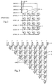
- Figure 1 illustrates a keyboard arrangement of this type that is realized according to the prior art.
- a keyboard matrix has separate output lines, here COL0 - COL4, and input lines, here ROW0 - ROW3, which are pulled-up inputs of a detector circuit (not shown), as indicated by reference number 10.
- switching means 11 connects a certain output line and a certain input line together, causing an interruption in said input line.
- a keyboard matrix scanning process begins where the output lines are written down by turn, and the status of the input lines is read each time. In this way the pressed key is finally identified.
- the number of keys that may be detected by means of this type of arrangement is equal to the product of the number of output and input lines. In the arrangement of figure 1, 20 keys may be detected by five output lines and four input lines, a total of nine lines 1 - 9.
- a purpose of the present invention is to produce a functionally and structurally simpler solution for realizing a keyboard arrangement of this type.
- detection of a pressed key by means of scanning is relatively time-consuming and the scanning software consumes memory capacity.
- the purpose of the present invention is to simplify detection of a pressed key.
- Another purpose of the present invention is to produce a keyboard arrangement that is well shielded against electrostatic discharges (ESD) and other electromagnetic interference (EMI). Electrostatic discharges may cause interference in mobile phones, for example, and most discharges of this type have been shown to enter a phone through the keyboard.
- ESD electrostatic discharges
- EMI electromagnetic interference
- Document GB-A-2 102 626 discloses a button with a contact pad that connects two underneath located contacts to a common ground.
- the two contacts are row and column contacts that form a row-common and column-common contact when contacted to the common ground. Any electrostatic discharge due to the user is coupled directly to the circuit earth minimizing susceptibility to electrostatic damage.
- a keyboard arrangement includes:
- the connecting means are a conductive plate-like part, which is connected to the ground plane and covers the whole keyboard.
- the part may be a metal plate or a conductive plastic plate.
- This implementation also provides excellent protection against electrostatic discharges and other interference. Another benefit, for example, when different mobile phone models have different keyboard layouts, is that a single printed circuit board may be realized having conductor patterns for the keyboard layouts of different models, and each model utilizes only its own switch board.
- the conductor lines of the conductor pattern are pulled-up inputs of the detector circuit, whereupon, as a response to any conductor line being connected to ground it is possible to detect the conductor lines that are connected to the ground plane and thereby identify the key that was pressed.
- a keyboard comprising:
- the total number of conductor lines is n
- each of said conductor lines is associated with n - 1 keys
- the total number of keys is ⁇ n x (n - 1) ⁇ /2.
- a method according to the present invention for identifying a pressed key in a keyboard arrangement includes:
- the status of the conductor lines is detected by means of a detector circuit to which the conductor lines are connected as pulled-up inputs, and as a response to one of the conductor lines being connected to the ground plane, the status of all the conductor lines is detected, and the key corresponding to the conductor lines that are connected to the ground plane is thus identified.
- the conductor lines are continuously polled, and the conductor lines that are connected to the ground plane are thus detected.
- n lines n*(n-1)/2 keys can be identified. This is clearly more than the number of keys that can be identified by means of the solution according to the prior art described above. In principle, it is just as easy to identify any combination of pulled-down lines by implementing the method of the present invention. Thus, a key can be identified based on just one or, for example, three or four pulled-down lines. Therefore, it is possible to further increase the number of keys identifiable with the same number of lines.
- Figure 1 presents a circuit diagram of a keyboard arrangement according to the prior art
- Figure 2 presents a circuit diagram of a keyboard arrangement according to the present invention corresponding to the keyboard arrangement of figure 1,
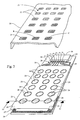
- Figure 3 presents a diagrammatic perspective view of an embodiment of a keyboard arrangement according to the present invention.
- Figure 4 is a diagrammatic cross-sectional view from IV - IV of figure 3.
- FIG. 2 presents a circuit diagram of a comparable keyboard arrangement according to the present invention, which, like the solution in figure 1, is based on nine conductor lines 1' - 9'. Here all the conductor lines are fitted with pull-up resistors 10, and they are pulled-up inputs of a detector circuit (not shown).
- the diagrammatically presented conductor pattern is arranged so that all possible pairs of conductor lines pass close to each other at a location where they may be connected together.
- Each said location is fitted with means to connect said conductor lines to a ground plane as a response to a pressing of a corresponding key.
- Said means are pictured as switches 12, which are capable of connecting the conductor lines to the ground plane 13.
- a key can be identified as follows, for example: an interruption is created in the detector circuit when any one of the conductor lines 1' - 9' is connected to ground, after which the status of all the lines is read and the key that was pressed is determined.
- Nine lines are used here to identify 36 keys, while correspondingly only 20 keys could be identified using the keyboard arrangement of figure 1.
- FIG. 3 diagrammatically presents an embodiment of a keyboard arrangement according to the present invention.
- Part of the shell of a mobile phone 20 and its keyboard 21, which comprises 20 keys, are diagrammatically shown at the top.
- the keyboard is placed over the arrangement shown at the bottom so that each key 22 lines up with a corresponding round zone 24.
- the keys have a known structure or other structure by which a key exerts a force on a zone 24 of the plate 23 below it when pressed.
- Three keys in the bottom row, which are indicated with markings A, B and C, are examined in more detail later.
- the plate 23, which is a conductive plate connected to a ground plane, covers the whole keyboard and thus forms a good shield against electrostatic discharges and other electromagnetic interference.
- the plate 23 Underneath the plate 23 is a printed circuit board 26 that has a conductor pattern 28 comprising conductor lines 1' - 7' and a ground plane 27. A detector circuit 29 is shown installed on the same printed circuit board, and the conductor lines 1' - 7' are connected to the detector circuit as pulled-up inputs.
- the plate 23 is a thin metal plate from which each key zone 24 is separated by means of curved openings so that only thin strips connect the key zones to the metal plate.
- the zones 24 are dome-shaped.
- the plate also has protruding embossments 25 formed by punching, for example, on its bottom side, which come into contact with corresponding regions 27 of the ground plane of the printed circuit board 26 when the plate 23 is installed and fastened in place.
- Figure 4 shows a diagrammatic cross-sectional view from IV - IV of figure 3, which illustrates the functioning of a keyboard arrangement according to the present invention in more detail.
- Lines 4', 5'; 4', 6' and 4', 7' of the conductor pattern of printed circuit board 26 are shown as examples underneath corresponding keys A, B and C and zones 24.
- Metal plate 23 is supported by embossments 25, which contact ground plane regions of the printed circuit board 26.
- the plate 23 may be kept apart from the conductor pattern of the printed circuit board by other means than embossments that contact the ground plane or similar supporting means. It is also possible that the plate 23 rests against an ordinary isolation layer, such as a solder resist coating, which covers most of the conductor pattern.
- An isolating plate with openings corresponding to the key zones may be located between the plate 23 and the printed circuit board comprising a conductor pattern.
- the zones 24 of plate 23 corresponding to the keys are dome-shaped. When a key B is pressed, a force P is exerted against a zone 24, the zone 24 bends downward and connects conductor lines 4' and 6' together and to the ground plane 27.
- the detector circuit 29 detects the conductor lines 4' and 6' connected to the ground plane 27, and thus identifies the pressed key as B.
- the pressed key B is identified by detecting the lines 4', 6' connected to the ground plane.
- the status of the conductor lines 1' - 7' is examined by means of a detector circuit 29 (figure 3), to which the conductor lines are connected as pulled-up inputs as shown by reference number 10 in figure 2.
- the status of all the conductor lines is examined, thus identifying the key corresponding to the conductor lines connected to the ground plane. This may be realized so that connecting any one of the conductor lines to ground causes an interruption in the detector circuit 29, after which the circuit examines which conductor lines are at ground potential.
- the method according to the present invention may also be realized by continuously polling the conductor lines, thus detecting which conductor lines are connected to the ground plane at a given moment.
- the present invention is not limited to said embodiments.
- An expert in the field understands that, for example, the means by which the conductor lines are connected to the ground plane may be realized in many different ways.
- the metal plate may be replaced by metallized plastic or plastic-based conductive polymer, for example.
- the shape and operating mechanism of the means may also vary. It is essential that the conductor lines corresponding to a key may be connected to a ground plane as a response to a pressing of the key.
- the base on which the conductor lines are formed may be advantageously realized by means of conventional printed circuit board technology, but it is clear that many other technologies for forming conductor patterns may also be used.
- a special detector circuit is presented above, whose inputs are the conductor lines.
- the detector circuit is integrated in an ASIC component, which also performs many other functions.
- the detector circuit may just as easily be located on a separate printed circuit board than the one on which the keyboard conductor pattern is located.
- the primary application of the present invention is a mobile phone, but it is clear that the keyboard arrangement according to the present invention also provides noticeable benefits in many other devices.
Landscapes
- Input From Keyboards Or The Like (AREA)
- Push-Button Switches (AREA)
- Telephone Set Structure (AREA)
Claims (14)
- Tastaturanordnung, die umfasst:wobei die Mittel bei jeder Taste zum Verbinden der Leiterleitungen miteinander Mittel (12, 24) sind, die in Reaktion auf ein Niederdrücken (P) der Taste (B) die Leiterleitungen (4', 6') mit der Masseebene (27) verbinden,eine Tastatur (21), die mehrere Tasten (22) aufweist,ein Leitermuster (28), in dem n Leiterleitungen (1'-7') so angeordnet sind, dass bei jeder Taste bestimmte Leiterleitungen (4', 5'; 4', 6'; 4', 7') miteinander verbunden werden können,Mittel (24) bei jeder Taste (A, B, C) zum Verbinden der bestimmten Leiterleitungen miteinander in Reaktion auf ein Niederdrücken (P) einer Taste (B),eine Masseebene (27) undeine Erfassungsschaltung (29), mit der die Leiterleitungen (1'-7') und die Masseebene (27) verbunden sind,
dadurch gekennzeichnet, dass jeder Taste (22) zwei Leiterleitungen (1' bis 7') zugeordnet sind und eine Leiterleitung der n Leiterleitungen über entsprechende Tasten mit jeder der anderen Leiterleitungen verbunden werden kann, so dass die Leiterleitung somit n - 1 Tasten zugeordnet ist. - Tastaturanordnung nach Anspruch 1, dadurch gekennzeichnet, dass die Verbindungsmittel ein leitendes plattenähnliches Teil (23) sind, das mit der Masseebene (27) verbunden ist und die gesamte Tastatur (21) abdeckt.
- Tastaturanordnung nach Anspruch 2, dadurch gekennzeichnet, dass das leitende plattenähnliche Teil (23) eine Metallplatte ist.
- Tastaturanordnung nach Anspruch 2, dadurch gekennzeichnet, dass das leitende plattenähnliche Teil (23) eine leitende Kunststoffplatte ist.
- Tastaturanordnung nach Anspruch 1, dadurch gekennzeichnet, dass die Leiterleitungen (1'-7') des Leitermusters (28) Spannungshochpegel-Eingänge einer Erfassungsschaltung (29) sind, wobei die Erfassungsschaltung (29) in Reaktion auf die Verbindung irgendeiner Leiterleitung mit der Masseplatte jene Leiterleitungen erfasst, die mit der Masseebene verbunden sind, und dadurch die Taste, die niedergedrückt wurde, identifiziert.
- Tastaturanordnung nach Anspruch 1, dadurch gekennzeichnet, dass die Leiterleitungen (1'-7') des Leitermusters (28) Spannungshochpegel-Eingänge der Erfassungsschaltung (29) sind, wobei die Erfassungsschaltung (29) die Eingänge ununterbrochen überwacht, um jene Leiterleitungen zu erfassen, die mit der Masseebene verbunden sind, und um dadurch eine niedergedrückte Taste zu identifizieren.
- Tastaturanordnung nach einem vorhergehenden Anspruch, dadurch gekennzeichnet, dass jede Leiterleitung der n Leiterleitungen über entsprechende Tasten mit jeder der anderen Leiterleitungen verbunden werden kann, so dass jede Leiterleitung n - 1 Tasten zugeordnet ist.
- Tastaturanordnung nach einem vorhergehenden Anspruch, dadurch gekennzeichnet, dass
die Gesamtzahl von Leiterleitungen (1' bis 7') n ist, wobei jede der Leiterleitungen (1' bis 7') n - 1 Tasten zugeordnet ist und die Gesamtzahl der Tasten {n_(n - 1)}/2 ist. - Tastaturanordnung nach einem vorhergehenden Anspruch, dadurch gekennzeichnet, dass alle Leiterleitungen mit Pullup-Widerständen (10) versehen sind und Spannungshochpegel-Eingänge der Erfassungsschaltung (29) sind.
- Mobiltelephon, das eine Tastaturanordnung nach einem der obigen Ansprüche enthält.
- Verfahren zum Identifizieren einer niedergedrückten Taste in einer Tastaturanordnung, die umfasst:wobei in dem Verfahren der Status der Leiterleitungen erfasst wird,eine Tastatur (21), die mehrere Tasten (22) aufweist,ein Leitermuster (28), in dem n Leiterleitungen (1'-7') so angeordnet sind, dass sie einzeln jeder Taste (A, B, C) entsprechen, wobei bestimmte Leiterleitungen (4', 5'; 4', 6'; 4', 7') miteinander verbunden werden können, undeine Masseebene (27), die getrennt von den Leiterleitungen vorgesehen ist,
die bestimmten Leiterleitungen (4', 6') mit der Masseebene (27) in Reaktion auf ein Niederdrücken (P) einer Taste (B) verbunden werden, und
die Leiterleitungen (4', 6'), die mit der Masseebene (27) verbunden sind, erfasst werden und somit die entsprechende Taste (B) identifiziert wird, dadurch gekennzeichnet, dass das Verfahren umfasst:wobei der Erfassungsschritt das Erfassen der zwei Leiterleitungen umfasst, die mit der Masseebene verbunden sind, wenn die bestimmte Taste (B) niedergedrückt wird.Zuordnen jeder Taste (22) zu zwei Leiterleitungen (1' bis 7'), undAnordnen der Leiterleitungen in der Weise, dass eine bestimmte Leiterleitung der n Leiterleitungen über entsprechende Tasten mit jeder der anderen Leiterleitungen verbunden werden kann, so dass diese bestimmte Leiterleitung n - 1 Tasten zugeordnet ist, - Verfahren nach Anspruch 11, dadurch gekennzeichnet, dass
der Status der Leiterleitungen (1'-7') durch eine Erfassungsschaltung (29) erfasst wird, mit der die Leiterleitungen als Spannungshochpegel-Eingänge verbunden sind,
in Reaktion auf die Verbindung einer der Leiterleitungen mit der Masseebene der Status aller Leiterleitungen erfasst wird und die Taste, die den Leiterleitungen entspricht, die mit der Masseebene verbunden sind, somit identifiziert wird. - Verfahren nach Anspruch 11, dadurch gekennzeichnet, dass die Leiterleitungen (1'-7') ununterbrochen abgefragt werden und somit die Leiterleitungen, die mit der Masseebene verbunden sind, erfasst werden.
- Verfahren nach Anspruch 11, dadurch gekennzeichnet, dass es umfasst:Anordnen der Leiterleitungen in der Weise, dass jede Leiterleitung der n Leiterleitungen über entsprechende Tasten mit jeder der anderen Leiterleitungen verbunden werden kann, wobei jede Leiterleitung somit n - 1 Tasten zugeordnet ist.
Applications Claiming Priority (2)
| Application Number | Priority Date | Filing Date | Title |
|---|---|---|---|
| FI963986A FI102119B1 (fi) | 1996-10-04 | 1996-10-04 | Näppäimistöjärjestely ja menetelmä painetun näppäimen tunnistamiseksi |
| FI963986 | 1996-10-04 |
Publications (3)
| Publication Number | Publication Date |
|---|---|
| EP0834993A2 EP0834993A2 (de) | 1998-04-08 |
| EP0834993A3 EP0834993A3 (de) | 1998-09-30 |
| EP0834993B1 true EP0834993B1 (de) | 2004-06-30 |
Family
ID=8546807
Family Applications (1)
| Application Number | Title | Priority Date | Filing Date |
|---|---|---|---|
| EP97660098A Expired - Lifetime EP0834993B1 (de) | 1996-10-04 | 1997-09-12 | Tastatur und Verfahren zur Identifizierung einer gedrückten Taste |
Country Status (5)
| Country | Link |
|---|---|
| US (1) | US5877709A (de) |
| EP (1) | EP0834993B1 (de) |
| JP (1) | JPH10161790A (de) |
| DE (1) | DE69729698T2 (de) |
| FI (1) | FI102119B1 (de) |
Families Citing this family (22)
| Publication number | Priority date | Publication date | Assignee | Title |
|---|---|---|---|---|
| DE19824149A1 (de) | 1998-05-29 | 1999-12-02 | Nokia Mobile Phones Ltd | Drehsteller für elektrische oder elektronische Geräte |
| FI109731B (fi) | 1998-06-02 | 2002-09-30 | Nokia Corp | Elektroniikkalaite ja ohjauselin |
| FI109732B (fi) | 1998-06-02 | 2002-09-30 | Nokia Corp | Elektroniikkalaite ja ohjauselin |
| FI104221B (fi) | 1998-06-30 | 1999-11-30 | Nokia Mobile Phones Ltd | Kaksiosainen elektroninen laite |
| JP2000347790A (ja) * | 1999-06-01 | 2000-12-15 | Alps Electric Co Ltd | キーボード装置 |
| US6323445B1 (en) | 2000-04-28 | 2001-11-27 | Microsoft Corporation | Membrane switch structure providing electrostatic discharge protection |
| US6577250B1 (en) | 2000-05-19 | 2003-06-10 | Microsoft Corporation | Resistance based keyboard key discrimination |
| US6621484B1 (en) | 2000-06-27 | 2003-09-16 | Microsoft Corporation | Keyboard key discrimination based on time division multiplexing |
| KR100337786B1 (ko) * | 2000-08-19 | 2002-05-24 | 윤종용 | 와이드 키패드 및 정전기 방지용 와이드 키패드 결합구조 |
| US6630927B2 (en) | 2001-02-15 | 2003-10-07 | Microsoft Corporation | Keyboard key discrimination employing drive line/sense line combinations and accomodating simultaneous key press conditions |
| ATE418743T1 (de) * | 2001-03-30 | 2009-01-15 | Ocg Technology Licensing Llc | Ringkernfaser |
| US6931125B2 (en) | 2001-07-10 | 2005-08-16 | Gregory N. Smallwood | Telephone equipment compatible, twelve button alphanumeric keypad |
| US6980135B2 (en) * | 2002-01-11 | 2005-12-27 | Alcor Micro, Corp. | Logic circuit using hardware to process keyboard scanning |
| KR100512374B1 (ko) * | 2003-01-27 | 2005-09-05 | 삼성전자주식회사 | 메탈돔 스위치의 키 패턴 연결장치 |
| DE10360241B4 (de) * | 2003-12-16 | 2006-04-27 | Visteon Global Technologies, Inc., Dearborn | Schaltmatrix für ein Eingabegerät |
| TWI324898B (en) * | 2004-11-23 | 2010-05-11 | Qisda Corp | Keyboard circuit with electrostatic discharge protection |
| ATE538428T1 (de) * | 2005-10-05 | 2012-01-15 | Imerj Ltd | Tragbares electronisches kommunikationsgerät mit metallischem tastenfeld |
| KR100747462B1 (ko) | 2006-01-04 | 2007-08-09 | 엘지전자 주식회사 | 이동단말기의 키 패드 장치 |
| FR2910652B1 (fr) * | 2006-12-21 | 2009-04-24 | Dav Sa | Module de commande electrique, en particulier pour vehicule automobile |
| TW200832196A (en) * | 2007-01-19 | 2008-08-01 | Inventec Appliances Corp | Press-type touch control pad device |
| KR101362514B1 (ko) * | 2007-10-17 | 2014-02-13 | 삼성전자주식회사 | 터치 키의 정전기 방전 장치 |
| EP4376040A1 (de) * | 2022-11-25 | 2024-05-29 | Siemens Aktiengesellschaft | Folientastatur für ein schutzgerät im bereich der elektroenergieübertragung und -verteilung |
Family Cites Families (12)
| Publication number | Priority date | Publication date | Assignee | Title |
|---|---|---|---|---|
| FR2370348A1 (fr) * | 1976-11-05 | 1978-06-02 | Leveille Marc | Contacteur matriciel pour affichage video notamment |
| GB2102626B (en) * | 1981-07-21 | 1985-06-05 | Standard Telephones Cables Ltd | Contact dimple pad |
| EP0094130B1 (de) * | 1982-05-07 | 1987-01-21 | Philips Electronics Uk Limited | Tastatureinrichtung zur Dateneinführung |
| JPS59105131A (ja) * | 1982-12-08 | 1984-06-18 | Toshiba Corp | 入出力回路装置 |
| US4667181A (en) * | 1983-07-15 | 1987-05-19 | Honeywell Inc. | Keyboard data input assembly |
| US4906993A (en) * | 1988-04-04 | 1990-03-06 | John Fluke Mfg. Co., Inc. | Keyboard scanner apparatus and method |
| GB8826340D0 (en) * | 1988-11-10 | 1988-12-14 | Ncr Co | Data entry keyboard apparatus |
| US5266949A (en) * | 1990-03-29 | 1993-11-30 | Nokia Mobile Phones Ltd. | Lighted electronic keyboard |
| FI88345C (fi) * | 1991-01-29 | 1993-04-26 | Nokia Mobile Phones Ltd | Belyst tastatur |
| JPH07307779A (ja) * | 1994-05-13 | 1995-11-21 | Oki Electric Ind Co Ltd | 携帯電話機のシールド構造 |
| US5554985A (en) * | 1995-06-14 | 1996-09-10 | United Microelectronics Corporation | Method for scanning keypad architecutre employing power source and ground of digital electronic devices |
| US5668544A (en) * | 1996-02-26 | 1997-09-16 | Holtek Microelectronics, Inc. | Compound type of keyboard detector |
-
1996
- 1996-10-04 FI FI963986A patent/FI102119B1/fi active IP Right Grant
-
1997
- 1997-09-12 EP EP97660098A patent/EP0834993B1/de not_active Expired - Lifetime
- 1997-09-12 DE DE69729698T patent/DE69729698T2/de not_active Expired - Lifetime
- 1997-10-03 JP JP9271554A patent/JPH10161790A/ja active Pending
- 1997-10-03 US US08/943,375 patent/US5877709A/en not_active Expired - Fee Related
Also Published As
| Publication number | Publication date |
|---|---|
| FI102119B (fi) | 1998-10-15 |
| US5877709A (en) | 1999-03-02 |
| DE69729698D1 (de) | 2004-08-05 |
| FI963986A0 (fi) | 1996-10-04 |
| FI102119B1 (fi) | 1998-10-15 |
| EP0834993A3 (de) | 1998-09-30 |
| FI963986L (fi) | 1998-04-05 |
| DE69729698T2 (de) | 2005-06-30 |
| JPH10161790A (ja) | 1998-06-19 |
| EP0834993A2 (de) | 1998-04-08 |
Similar Documents
| Publication | Publication Date | Title |
|---|---|---|
| EP0834993B1 (de) | Tastatur und Verfahren zur Identifizierung einer gedrückten Taste | |
| CA1241363A (en) | Laminate switch assembly having improved tactile feel and improved reliability of operation | |
| KR0142363B1 (ko) | 멤브레인 스위치 | |
| US7176894B2 (en) | Double-sided keyboard for use in an electronic device | |
| US4456800A (en) | Planar contact array switch having improved ground path for dissipating electrostatic discharges | |
| US5986228A (en) | Movable contact unit for panel switch and panel switch using the same | |
| CA1131733A (en) | Keyboard assembly and keyboard switch | |
| CN100555868C (zh) | 符合于弧形表面的柔性触摸板传感器网格 | |
| US9032222B2 (en) | Secure point of sale terminal | |
| US6630925B1 (en) | Double-sided keyboard having two keymats and one activation mat | |
| US4376238A (en) | Electrical devices | |
| US6323445B1 (en) | Membrane switch structure providing electrostatic discharge protection | |
| CA2208477A1 (en) | Electrical connector with shielding | |
| WO2010082190A1 (en) | Secure point of sale terminal | |
| KR20060113978A (ko) | 인쇄가능한 전자기계 입력 수단 및 그와 같은 입력 수단을포함하는 전자 디바이스 | |
| GB2100517A (en) | Electric push button switch | |
| US4207444A (en) | Planar multiple switch | |
| US5241695A (en) | Molded shield with integral key switch circuitry | |
| US7102086B2 (en) | Switch arrangement | |
| GB2071420A (en) | Retractive Mechanical Switches | |
| JPH1039993A (ja) | 透明タッチパネル及びそれを利用した入力装置 | |
| CN2248385Y (zh) | 可同时为电脑、电话使用的复合键盘 | |
| EP0238989B1 (de) | Kapazitätsschaltvorrichtung für Tastenfeld | |
| CN206331326U (zh) | 电子装置 | |
| JP4305014B2 (ja) | 携帯電話機および移動方向検出装置 |
Legal Events
| Date | Code | Title | Description |
|---|---|---|---|
| PUAI | Public reference made under article 153(3) epc to a published international application that has entered the european phase |
Free format text: ORIGINAL CODE: 0009012 |
|
| AK | Designated contracting states |
Kind code of ref document: A2 Designated state(s): DE FR GB IT |
|
| AX | Request for extension of the european patent |
Free format text: AL;LT;LV;RO;SI |
|
| PUAL | Search report despatched |
Free format text: ORIGINAL CODE: 0009013 |
|
| AK | Designated contracting states |
Kind code of ref document: A3 Designated state(s): AT BE CH DE DK ES FI FR GB GR IE IT LI LU MC NL PT SE |
|
| 17P | Request for examination filed |
Effective date: 19990330 |
|
| AKX | Designation fees paid |
Free format text: DE FR GB IT |
|
| RAP1 | Party data changed (applicant data changed or rights of an application transferred) |
Owner name: NOKIA CORPORATION |
|
| 17Q | First examination report despatched |
Effective date: 20030211 |
|
| GRAP | Despatch of communication of intention to grant a patent |
Free format text: ORIGINAL CODE: EPIDOSNIGR1 |
|
| GRAS | Grant fee paid |
Free format text: ORIGINAL CODE: EPIDOSNIGR3 |
|
| GRAA | (expected) grant |
Free format text: ORIGINAL CODE: 0009210 |
|
| AK | Designated contracting states |
Kind code of ref document: B1 Designated state(s): DE FR GB IT |
|
| REG | Reference to a national code |
Ref country code: GB Ref legal event code: FG4D |
|
| REF | Corresponds to: |
Ref document number: 69729698 Country of ref document: DE Date of ref document: 20040805 Kind code of ref document: P |
|
| ET | Fr: translation filed | ||
| PLBE | No opposition filed within time limit |
Free format text: ORIGINAL CODE: 0009261 |
|
| STAA | Information on the status of an ep patent application or granted ep patent |
Free format text: STATUS: NO OPPOSITION FILED WITHIN TIME LIMIT |
|
| 26N | No opposition filed |
Effective date: 20050331 |
|
| PGFP | Annual fee paid to national office [announced via postgrant information from national office to epo] |
Ref country code: GB Payment date: 20090909 Year of fee payment: 13 |
|
| PGFP | Annual fee paid to national office [announced via postgrant information from national office to epo] |
Ref country code: DE Payment date: 20090910 Year of fee payment: 13 |
|
| PGFP | Annual fee paid to national office [announced via postgrant information from national office to epo] |
Ref country code: IT Payment date: 20090915 Year of fee payment: 13 Ref country code: FR Payment date: 20091012 Year of fee payment: 13 |
|
| GBPC | Gb: european patent ceased through non-payment of renewal fee |
Effective date: 20100912 |
|
| PG25 | Lapsed in a contracting state [announced via postgrant information from national office to epo] |
Ref country code: IT Free format text: LAPSE BECAUSE OF NON-PAYMENT OF DUE FEES Effective date: 20100912 |
|
| REG | Reference to a national code |
Ref country code: FR Ref legal event code: ST Effective date: 20110531 |
|
| REG | Reference to a national code |
Ref country code: DE Ref legal event code: R119 Ref document number: 69729698 Country of ref document: DE Effective date: 20110401 |
|
| PG25 | Lapsed in a contracting state [announced via postgrant information from national office to epo] |
Ref country code: FR Free format text: LAPSE BECAUSE OF NON-PAYMENT OF DUE FEES Effective date: 20100930 Ref country code: DE Free format text: LAPSE BECAUSE OF NON-PAYMENT OF DUE FEES Effective date: 20110401 |
|
| PG25 | Lapsed in a contracting state [announced via postgrant information from national office to epo] |
Ref country code: GB Free format text: LAPSE BECAUSE OF NON-PAYMENT OF DUE FEES Effective date: 20100912 |