EP0831684A2 - Verpackung für Leistungselektronik - Google Patents
Verpackung für Leistungselektronik Download PDFInfo
- Publication number
- EP0831684A2 EP0831684A2 EP97116569A EP97116569A EP0831684A2 EP 0831684 A2 EP0831684 A2 EP 0831684A2 EP 97116569 A EP97116569 A EP 97116569A EP 97116569 A EP97116569 A EP 97116569A EP 0831684 A2 EP0831684 A2 EP 0831684A2
- Authority
- EP
- European Patent Office
- Prior art keywords
- edge
- fuselage
- packaging according
- packaging
- lid
- Prior art date
- Legal status (The legal status is an assumption and is not a legal conclusion. Google has not performed a legal analysis and makes no representation as to the accuracy of the status listed.)
- Withdrawn
Links
- 238000004806 packaging method and process Methods 0.000 title claims abstract description 26
- 239000004065 semiconductor Substances 0.000 claims description 16
- 239000004020 conductor Substances 0.000 claims description 12
- 239000010410 layer Substances 0.000 claims description 12
- 239000004576 sand Substances 0.000 claims description 11
- 229920000642 polymer Polymers 0.000 claims description 9
- 239000002245 particle Substances 0.000 claims description 6
- 239000012790 adhesive layer Substances 0.000 claims description 5
- 239000002184 metal Substances 0.000 claims description 5
- 229910052751 metal Inorganic materials 0.000 claims description 5
- 239000011230 binding agent Substances 0.000 claims description 4
- 239000000203 mixture Substances 0.000 claims description 4
- 230000001427 coherent effect Effects 0.000 claims description 2
- 229910000831 Steel Inorganic materials 0.000 claims 1
- 229910052782 aluminium Inorganic materials 0.000 claims 1
- XAGFODPZIPBFFR-UHFFFAOYSA-N aluminium Chemical compound [Al] XAGFODPZIPBFFR-UHFFFAOYSA-N 0.000 claims 1
- 239000008187 granular material Substances 0.000 claims 1
- 239000010959 steel Substances 0.000 claims 1
- 230000002093 peripheral effect Effects 0.000 abstract 3
- RYGMFSIKBFXOCR-UHFFFAOYSA-N Copper Chemical compound [Cu] RYGMFSIKBFXOCR-UHFFFAOYSA-N 0.000 description 9
- 229910052802 copper Inorganic materials 0.000 description 9
- 239000010949 copper Substances 0.000 description 9
- 230000000694 effects Effects 0.000 description 3
- 238000009413 insulation Methods 0.000 description 3
- 239000004593 Epoxy Substances 0.000 description 1
- 230000015572 biosynthetic process Effects 0.000 description 1
- 238000001816 cooling Methods 0.000 description 1
- 238000002788 crimping Methods 0.000 description 1
- 239000000945 filler Substances 0.000 description 1
- 238000002955 isolation Methods 0.000 description 1
- 229920002959 polymer blend Polymers 0.000 description 1
- 230000005855 radiation Effects 0.000 description 1
- 239000011347 resin Substances 0.000 description 1
- 229920005989 resin Polymers 0.000 description 1
- 238000005728 strengthening Methods 0.000 description 1
Images
Classifications
-
- H—ELECTRICITY
- H05—ELECTRIC TECHNIQUES NOT OTHERWISE PROVIDED FOR
- H05K—PRINTED CIRCUITS; CASINGS OR CONSTRUCTIONAL DETAILS OF ELECTRIC APPARATUS; MANUFACTURE OF ASSEMBLAGES OF ELECTRICAL COMPONENTS
- H05K5/00—Casings, cabinets or drawers for electric apparatus
- H05K5/10—Casings, cabinets or drawers for electric apparatus comprising several parts forming a closed casing
-
- H—ELECTRICITY
- H05—ELECTRIC TECHNIQUES NOT OTHERWISE PROVIDED FOR
- H05K—PRINTED CIRCUITS; CASINGS OR CONSTRUCTIONAL DETAILS OF ELECTRIC APPARATUS; MANUFACTURE OF ASSEMBLAGES OF ELECTRICAL COMPONENTS
- H05K7/00—Constructional details common to different types of electric apparatus
- H05K7/14—Mounting supporting structure in casing or on frame or rack
- H05K7/1422—Printed circuit boards receptacles, e.g. stacked structures, electronic circuit modules or box like frames
- H05K7/1427—Housings
- H05K7/1432—Housings specially adapted for power drive units or power converters
- H05K7/14322—Housings specially adapted for power drive units or power converters wherein the control and power circuits of a power converter are arranged within the same casing
Definitions
- the technical field of the invention is the packaging of power electronics should be quick, safe and inexpensive.
- the folded edge of the hat-shaped cover can be L-shaped (claim 2), the laterally protruding leg of the L-shaped folded edge when closing on the rim of the fuselage trough, which also projects laterally as a support (claim 3) lies on.
- the remaining vertical leg of the L-shaped contact leg of the hat-shaped cover is then a single fold with a flat pressed Clamping flanged (claim 4), so that the can-like packaging in the form of a rectangular container made of deep-drawn sheet metal, which has a seam all the way around, which is close to the main structure of the power electronics lies.
- Additional boards can be added Components in one direction vertical to the plane of the main power electronics assembly attached to the top of this vertical Additional boards (claim 9) to provide electrical connections through openings step through the top of the hat-shaped lid.
- the connections are made here of the high current, one input voltage and one output voltage, if necessary also DC link voltage, i.e. the connection of the feed network and the connection of the machine to be controlled.
- the main level of power electronics (claim 10) is in the flat trough-shaped fuselage used that they have a good cooling effect to the bottom of the Fuselage allows.
- a thermally conductive thicker plate can be provided which can be made of copper, for example, and on which is insulated Islands the power electronics components (power diodes, power transistors, GTOs, other common power semiconductors) can be attached in an insulating manner, surrounded by one that enables the electrical connections of the control Circuit board that can be designed flexibly. Connections from and to the Power semiconductors are made with bond wires that are arranged to the side Connecting pins lead from which thicker connecting lines directly to the above mentioned terminals are placed (in the vertical direction) or over the vertically standing additional boards are placed upwards.
- control currents and measuring currents can be guided via the above-mentioned flexible Circuit board, carries the conductor tracks and has cut out openings, through which the power semiconductors that are directly on the bottom of the tub or on the Copper plate are attached, protrude.
- these conductor tracks can also be used directly be attached to the bottom of the fuselage pan if an insulating adhesive layer that Resin character has been used as an intermediate layer to both Fastening function as well as insulation function. Then there is a separate one Isolation board not required and the entire structure of the power electronics Control currents and load currents can be placed directly on the bottom surface of the tub to be appropriate.
- Heat conduction to the heat sink at the bottom of the deep-drawn packaging made of sheet metal is achieved with a loosely filled sand / polymer mixture (claim 7, Claim 8).
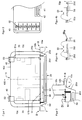
- Figure 1 is a sectional side view of the container 10 with a hat-shaped lid which has an upper surface 10d and four side walls 10c which are aligned vertically. At the end of these side walls an L-shaped (circumferential) folding leg 10b, 10a is provided, the horizontal section 10b of which rests on a support leg 20b of the flat trunk trough 20.
- the cover 10 is put on - when the hat-shaped cover is slipped over the trough base 20 equipped with a circuit board structure 50, 51 and the associated vertical additional boards 51a, 51b - the vertical leg 10a slides past the end of the horizontal leg 20b of the floor trough. The end of the touchdown is reached when the horizontal pair of legs 10b, 20b rests on one another.
- FIGS. 4a and 4b showing possibilities such as this Structure may look in detail, which structure is generally referred to as "circuit board", to express that a circuit board with components could be provided per se, but this circuit board no longer necessarily has an epoxy base and a conductor track attached to it , but partially thermally conductive, partially electrically insulating and in detail in several layers but essentially on one level.
- FIG. 4a illustrates the mounting on a copper plate 30, which can also be seen in FIG. 1 as an intermediate layer to "circuit board 50" on which the power electronics components 60 are shown schematically.
- This mechanically stable plate 30, which is thermally conductive, is placed on the bottom 20d of the tub 20.
- An intermediate layer can be provided for the elastic compensation of unevenness and for avoiding the formation of gas bubbles in the thermally conductive path.
- a structure is provided on the conductive plate 30, which consists of a flexible circuit board that has island openings through which the power semiconductors 60 protrude, which are firmly attached to the copper plate 30 on their own insulating islands 50i.
- the flexible conductor track 50p enables the control currents and signal currents to be fed to the power semiconductors, while the power currents are conducted directly via bond wires to thicker connecting lines 70 in FIG. 1 in order to reach the power connection terminals 52, 53.
- the circuit board 50p is therefore insulated, but lies loosely or lightly fastened only on the copper plate 30, while a respective power semiconductor 60 is firmly and permanently attached to the copper plate 30 via an insulation island 50i made of an insulating adhesive layer.
- FIG. 4b shows the direct structure of the power semiconductors 60 on the bottom 20d of the fuselage trough 20, also by means of an insulating layer 50i, which has an island-like character, in each case with reference to the power semiconductor 60, which it is intended to insulate electrically from the bottom surface 20d, but which it thermally connects conductively to this bottom surface 20d.
- the conductor path guidance on a flexible, essentially coherent circuit board 50p with openings for the islands is indicated in the enlarged detail around the power semiconductor island 50i; it thus surrounds the power semiconductor to be controlled.
- the loose or slightly attached flexible (thin) circuit board 50p can also be designed such that it is replaced by an insulating layer similar to the insulating adhesive layer 50i of the power semiconductor 60, which is then directly on the copper plate 30 or directly according to FIG 4b can be attached to the bottom 20d of the fuselage pan. Then both the power semiconductors 60 via the insulating islands 50i, and the conductor track routing via the insulating layers are attached directly to the bottom 20d of the fuselage trough and allow a cost-effective, low-profile and thermally directly connected structure to the bottom.
- FIG. 3 illustrates the edge area of the structure of the “circuit board 50” shown in detail in FIGS. 4a and 4b , the copper plate 30 being shown, which has mechanically strengthening and thermally conductive properties to the bottom 20d of the fuselage trough.
- a slightly outwardly inclined connecting leg 20a leads from the bottom 20d into the horizontal support leg 20b of the fuselage trough edge, which serves to form the locking fold 10b, 20b, 10a.
- the force effect of the folding on the leg 10a is symbolized by F.
- the leg 10a can be slightly longer than the support leg 20b in order to achieve a clamping effect on the connecting leg 20a on the inside.
- FIG. 2 shows the top view which allows access to the connection terminals 52, which transmit high currents, through openings on the upper plate 10d of the hat-shaped cover 10.
- the opening 40 is rectangular and slightly larger than the plastic insulation or an insulating block of the connecting terminals 52, which in FIG. 1 are partly led through the connecting cables 70 of large diameter to the power electronics level 50 in the fuselage trough 20, but which can also have a connection to the vertically standing boards 51a, 51b with their conductor tracks.
- control technology and the measured value acquisition take place through a further elongated opening 41 in the cover panel 10d, through which a multiple connector plug 42 for low current can protrude.
- this opening is made perpendicular to the two power electronics openings 40 arranged on the edge in the cover surface 10d.
- a mixture of sand and a polymer as a binder can be found in the packaging be filled in loosely before the folded edge B is closed. This will make one Overall thermal conductivity is produced, which all components reasonably thermally conductive with the metallic outer surfaces of the can-like housing connects.
- this mixture of sand and polymer can be elastic Particles are inserted that have an elastic bias on all components and thus allow a mechanical fixing when closing the flanged edge B.
- the mixture of sand and polymer consists mainly of sand and has a maximum 65% by weight thereof. Up to 30% binder in the form of mentioned polymer and about 5% of the elastic particles, the Definition of about 5% a range from 0 to 10% (especially around 5%) of this should describe elastic particles, the rest is filled with sand or polymer.
- the technical field of the invention is the packaging of power electronics should be quick, safe and inexpensive.
- A is proposed for this Packaging for a circuit arranged on a carrier surface (50; 50i; 50p) Power electronics (60), which packaging a deep-drawn hat-shaped lid (10) and has a flat trough-shaped body (20), the edge (20a, 20b) by folding or flanging (B) one attached to the edge of the lid Folded edge (10a, 10b) around the edge (20b) of the fuselage pan (20) is closed.
- the "Packaging” formed in this way is essentially a housing in which the hull is flat and the lid is one of the height of the components or vertically inserted boards has the appropriate dimension.
Landscapes
- Engineering & Computer Science (AREA)
- Microelectronics & Electronic Packaging (AREA)
- Insulated Metal Substrates For Printed Circuits (AREA)
- Casings For Electric Apparatus (AREA)
Abstract
Description
- Figur 1
- ist eine Seitenansicht eines Behältnisses aus tiefgezogenem Metallblech mit hutförmigem Deckel 10 und flacher Wanne 20 als Rumpf und einem umlaufenden Bördelrand B.
- Figur 2
- ist eine Aufsicht auf die Verpackung gemäß Figur 1, in der die linke Hälfte mit der durch eine langgestreckte Öffnung 40 zugängliche Anschluß-Klemmenleiste 52 dargestellt ist und ein Teil der dazu senkrecht verlaufenden Anschlußleiste 42 gezeigt ist, die durch eine weitere Öffnung 41 im hutförmigen Deckel 10 zugänglich ist, um Steuerströme, Meßströme und andere Signale zuführen und abnehmen zu können.
- Figur 3
- ist eine vergrößerte Teilansicht des Randbereiches der Ebene der Leistungselektronik von Figur 1, in der der aus drei Blechlagen bestehende Falzrand B verdeutlicht wird, dessen Umfalzen mit dem Richtungsvektor F symbolisiert wird.
- Figur 4a, Figur 4b
- sind zwei Aufbauten in der Leistungselektronik-Ebene, einmal mit einer Kupferplatte 30 als mechanisch festem Träger des Leistungsaufbaus und einmal mit einer direkten Anbringung der Leistungselektronik-Komponenten 60 und der Leiterbahnführung auf dem Boden 20d der Rumpfwanne 20.
Claims (13)
- Verpackung für eine auf einer Platine (50;50i;50p) angeordnete Schaltung der Leistungselektronik (60), welche Verpackung einen tiefgezogenen hutförmigen Deckel (10;10a,10b,10c) und einen flachen wannenförmigen Rumpf (20) aufweist, die randseitig durch Umfalzen oder Bördeln (F) eines am Deckelrand angebrachten Falzrandes (10a,10b) um den Rand (20b) der Rumpfwanne (20) verschlossen ist (B).
- Verpackung nach Anspruch 1, bei der der Falzrand des Deckels (10) L-förmig (10a,10b) ist, mit einem seitlich abragenden Anlageschenkel (10b) und einem sich daran anschließenden axial (100) gerichteten Falzschenkel (10a).
- Verpackung nach Anspruch 2, bei der der Anlageschenkel (10b) so gestaltet ist, daß er nach Überstülpen des Deckels (10;10a,10b,10c) über die Schaltung (50,60) und nach Vorbeigleiten des Falzschenkels (10a) des Deckelrandes (10a,10b) an dem Rand (20b) der Rumpfwanne (20) flach auf einem seitlich abragenden Auflagerand (20b) der Rumpfwanne aufliegt.
- Verpackung nach einem der vorigen Ansprüche, bei der der Falz ein Einfachfalz (B) ist, insb. nur aus der flächengepreßten Klemmung einer oberen Deckelrandlage, einer Rumpflage und einer unteren Deckelrandlage (10b,20b,10a) besteht.
- Verpackung nach einem der vorigen Ansprüche, bei der der Deckel (10) und der Rumpf (20) aus Blech, insb. Aluminium- oder Stahlblech tiefgezogen gefertigt ist.
- Vorrichtung nach einem der vorigen Ansprüche, bei der die Bodenwanne (20) flach ist und eine leitende dickere Platte (30) aufnimmt.
- Verpackung nach einem der vorigen Ansprüche, bei der eine Mischung aus Sand und einem Polymer als Bindemittel in der Verpackung lose eingefüllt ist, insb. enthaltend etwa 0% bis 10% elastische Partikel, wie Gummigranulate.
- Verpackung nach Anspruch 7, bei der mehr Sand als Polymer (Kunststoff) enthalten ist und erst der Sand und dann das Polymer eingefüllt wird, wobei maximal 65% Sand, 30% Bindemittel und etwa 5% elastische Partikel enthalten sind.
- Verpackung nach einem der vorigen Ansprüche, bei der im Deckel (10) auf dessen oberer Flachseite (10d) Öffnungen (40,41) vorgesehen sind, durch die zumindest zwei elektrische Anschlußklemmenleisten (52,53;42) erreichbar sind, um Starkstrom und Steuerströme getrennt zuführen zu können.
- Verpackung nach einem der vorigen Ansprüche, bei der(a) als elektrisch isolierende Platine (50) Leistungselektronik-Komponenten (60) - umgeben von einem flexiblen Leiterbahnträger (50p) - elektrisch isoliert aber thermisch leitend (50i) fest an einer dickeren Platte (30) und diese am Boden (20d) der Rumpfwanne (20) elastisch angepresst ist; oder(b) ein Mehrlagen-Bodenaufbau dadurch gebildet wird, daß direkt auf dem Boden (20d) des wannenförmigen Rumpfes (20) eine thermisch leitende aber elektrisch isolierende Klebstoffschicht (50i;50p) aufgebracht ist, um Leiterbahnführungen und zu kühlende Halbleiter (60) fest am Boden (20d) des Rumpfes anzubringen und gleichwohl elektrisch zu isolieren.
- Verpackung nach Anspruch 10, bei der am Boden (20d) der Bodenwanne (20) ein Kühlkörper außenseitig thermisch leitend angebracht ist.
- Verpackung nach Anspruch 10 oder 11, bei der die Klebstoffschicht (50i) inselweise dort vorgesehen ist, wo ein Leistungshalbleiter (60) am Wannenboden (20d) direkt oder über die dickere Platte (30) indirekt angebracht ist.
- Verpackung nach Anspruch 12, bei der die elektrisch isolierenden Inseln (50i) umgeben sind von einem - weitgehend zusammenhängenden, mit Öffnungen für die Inseln ausgestatteten - flexiblen Leiterbahnträger (50p), der oberseitig Leiterbahnen trägt und unterseitig auf dem Wannenboden (20d) oder der dickeren Platte (30) anliegend angebracht ist.
Applications Claiming Priority (6)
| Application Number | Priority Date | Filing Date | Title |
|---|---|---|---|
| DE19638996 | 1996-09-23 | ||
| DE19638996 | 1996-09-23 | ||
| DE19643671 | 1996-10-22 | ||
| DE19643671 | 1996-10-22 | ||
| DE19650318 | 1996-12-04 | ||
| DE19650318A DE19650318C2 (de) | 1996-09-23 | 1996-12-04 | Gehäuse aus Metallblech für eine Schaltung der Leistungselektronik |
Publications (2)
| Publication Number | Publication Date |
|---|---|
| EP0831684A2 true EP0831684A2 (de) | 1998-03-25 |
| EP0831684A3 EP0831684A3 (de) | 1998-05-13 |
Family
ID=27216672
Family Applications (1)
| Application Number | Title | Priority Date | Filing Date |
|---|---|---|---|
| EP97116569A Withdrawn EP0831684A3 (de) | 1996-09-23 | 1997-09-23 | Verpackung für Leistungselektronik |
Country Status (1)
| Country | Link |
|---|---|
| EP (1) | EP0831684A3 (de) |
Cited By (1)
| Publication number | Priority date | Publication date | Assignee | Title |
|---|---|---|---|---|
| WO2020178131A1 (de) | 2019-03-04 | 2020-09-10 | Audi Ag | Direkte kühlung eines stromrichters durch verwendung einer geprägten platte |
Family Cites Families (5)
| Publication number | Priority date | Publication date | Assignee | Title |
|---|---|---|---|---|
| DE3528291A1 (de) * | 1985-08-07 | 1987-02-19 | Kernforschungsz Karlsruhe | Anordnung zur kuehlung elektronischer bauelemente |
| DE4132875A1 (de) * | 1991-10-03 | 1993-04-08 | Klaschka Ind Elektronik | Gehaeuseeinheit |
| DE4221137A1 (de) * | 1992-06-27 | 1994-01-05 | Bosch Gmbh Robert | Elektrisches Gerät, insbesondere Schalt- und/oder Steuergerät für Kraftfahrzeuge |
| KR100190154B1 (ko) * | 1994-06-16 | 1999-06-01 | 가나이 쓰도무 | 인버터 장치 |
| DE19548723A1 (de) * | 1995-12-23 | 1997-06-26 | Bosch Gmbh Robert | Gehäuse zur Aufnahme von elektronischen Bauelementen |
-
1997
- 1997-09-23 EP EP97116569A patent/EP0831684A3/de not_active Withdrawn
Non-Patent Citations (1)
| Title |
|---|
| None |
Cited By (2)
| Publication number | Priority date | Publication date | Assignee | Title |
|---|---|---|---|---|
| WO2020178131A1 (de) | 2019-03-04 | 2020-09-10 | Audi Ag | Direkte kühlung eines stromrichters durch verwendung einer geprägten platte |
| US12160982B2 (en) | 2019-03-04 | 2024-12-03 | Audi Ag | Direct cooling of a power converter by using a stamped plate |
Also Published As
| Publication number | Publication date |
|---|---|
| EP0831684A3 (de) | 1998-05-13 |
Similar Documents
| Publication | Publication Date | Title |
|---|---|---|
| DE10056832B4 (de) | Halbleiterbauteil-Moduleinheit | |
| EP4070629B1 (de) | Wechselrichter mit kompakter bauform | |
| DE19854180A1 (de) | Modulgehäuse für Halbleiterbauteile | |
| DE69417300T2 (de) | Zusammengesetzte Leiterplatte, Halbleiterleistungsmodul mit dieser zusammengesetzten Leiterplatte und Herstellungsmethode dafür | |
| DE102009011234B4 (de) | Elektronische Baugruppe | |
| DE69635440T2 (de) | Halbleiteranordnung mit einem Schaltungssubstrat und einem Gehäuse | |
| WO1993005635A1 (de) | Elektrisches gerät, insbesondere schalt- und steuergerät für kraftfahrzeuge | |
| EP0951131A2 (de) | Electric drive unit consisting of an electric motor and of an electronic unit | |
| EP0785708A1 (de) | Anordnung zum Schutz elektrischer und elektronischer Bauelmente vor elektrostatischen Entladungen | |
| EP0368143A2 (de) | Elektronisches Steuergerät | |
| DE4305793A1 (de) | Leistungsmodul | |
| EP0597144A1 (de) | Hybride leistungselektronische Anordnung | |
| DE112016004427B4 (de) | Schaltungsanordnung und elektrischer verteiler | |
| DE4021871A1 (de) | Hochintegriertes elektronisches bauteil | |
| DE102013212263A1 (de) | Elektrische Schaltungsanordnung | |
| DE102021110983A1 (de) | EMV-Filtervorrichtung aufweisend eine laminierte Leiterstruktur; sowie Leistungselektronikmodul | |
| DE102020216477A1 (de) | Leistungsmodul | |
| EP0994557B1 (de) | Umrichter mit niederinduktivem Kondensator im Zwischenkreis | |
| EP0639940A1 (de) | Schaltungsanordnung für Kraftfahrzeuge | |
| DE4338277C2 (de) | Flüssigkeitsgekühltes Stromrichtermodul mit Beschaltungsbauelementen für abschaltbare Leistungshalbleiter | |
| DE10122191A1 (de) | Halbleiterbauelement mit einem Halbleiterkörper und einem Gehäuse | |
| EP0831684A2 (de) | Verpackung für Leistungselektronik | |
| DE102021110988A1 (de) | EMV-Filtervorrichtung mit einer zur Abschirmung dienenden Abdeckung; sowie Leistungselektronikmodul | |
| DE19650318C2 (de) | Gehäuse aus Metallblech für eine Schaltung der Leistungselektronik | |
| EP0793407B1 (de) | Elektronische Schalteinrichtung, insbesondere elektronisches Relais, für Steckmontage |
Legal Events
| Date | Code | Title | Description |
|---|---|---|---|
| PUAI | Public reference made under article 153(3) epc to a published international application that has entered the european phase |
Free format text: ORIGINAL CODE: 0009012 |
|
| AK | Designated contracting states |
Kind code of ref document: A2 Designated state(s): DE FR GB IT |
|
| PUAL | Search report despatched |
Free format text: ORIGINAL CODE: 0009013 |
|
| AK | Designated contracting states |
Kind code of ref document: A3 Designated state(s): AT BE CH DE DK ES FI FR GB GR IE IT LI LU MC NL PT SE |
|
| 17P | Request for examination filed |
Effective date: 19981111 |
|
| AKX | Designation fees paid |
Free format text: DE FR GB IT |
|
| RBV | Designated contracting states (corrected) |
Designated state(s): DE FR GB IT |
|
| RAP1 | Party data changed (applicant data changed or rights of an application transferred) |
Owner name: BAYSIDE CONTROLS GMBH |
|
| GRAP | Despatch of communication of intention to grant a patent |
Free format text: ORIGINAL CODE: EPIDOSNIGR1 |
|
| STAA | Information on the status of an ep patent application or granted ep patent |
Free format text: STATUS: THE APPLICATION IS DEEMED TO BE WITHDRAWN |
|
| 18D | Application deemed to be withdrawn |
Effective date: 20040602 |