EP0828174A2 - Dispositif de conversion de longueur d'onde optique et circuit de détection de phase d'impulsions optiques - Google Patents
Dispositif de conversion de longueur d'onde optique et circuit de détection de phase d'impulsions optiques Download PDFInfo
- Publication number
- EP0828174A2 EP0828174A2 EP97114500A EP97114500A EP0828174A2 EP 0828174 A2 EP0828174 A2 EP 0828174A2 EP 97114500 A EP97114500 A EP 97114500A EP 97114500 A EP97114500 A EP 97114500A EP 0828174 A2 EP0828174 A2 EP 0828174A2
- Authority
- EP
- European Patent Office
- Prior art keywords
- light
- optical
- wavelength
- original signal
- absorptive
- Prior art date
- Legal status (The legal status is an assumption and is not a legal conclusion. Google has not performed a legal analysis and makes no representation as to the accuracy of the status listed.)
- Withdrawn
Links
Images


Classifications
-
- G—PHYSICS
- G02—OPTICS
- G02F—OPTICAL DEVICES OR ARRANGEMENTS FOR THE CONTROL OF LIGHT BY MODIFICATION OF THE OPTICAL PROPERTIES OF THE MEDIA OF THE ELEMENTS INVOLVED THEREIN; NON-LINEAR OPTICS; FREQUENCY-CHANGING OF LIGHT; OPTICAL LOGIC ELEMENTS; OPTICAL ANALOGUE/DIGITAL CONVERTERS
- G02F2/00—Demodulating light; Transferring the modulation of modulated light; Frequency-changing of light
- G02F2/004—Transferring the modulation of modulated light, i.e. transferring the information from one optical carrier of a first wavelength to a second optical carrier of a second wavelength, e.g. all-optical wavelength converter
-
- G—PHYSICS
- G02—OPTICS
- G02F—OPTICAL DEVICES OR ARRANGEMENTS FOR THE CONTROL OF LIGHT BY MODIFICATION OF THE OPTICAL PROPERTIES OF THE MEDIA OF THE ELEMENTS INVOLVED THEREIN; NON-LINEAR OPTICS; FREQUENCY-CHANGING OF LIGHT; OPTICAL LOGIC ELEMENTS; OPTICAL ANALOGUE/DIGITAL CONVERTERS
- G02F1/00—Devices or arrangements for the control of the intensity, colour, phase, polarisation or direction of light arriving from an independent light source, e.g. switching, gating or modulating; Non-linear optics
- G02F1/01—Devices or arrangements for the control of the intensity, colour, phase, polarisation or direction of light arriving from an independent light source, e.g. switching, gating or modulating; Non-linear optics for the control of the intensity, phase, polarisation or colour
- G02F1/015—Devices or arrangements for the control of the intensity, colour, phase, polarisation or direction of light arriving from an independent light source, e.g. switching, gating or modulating; Non-linear optics for the control of the intensity, phase, polarisation or colour based on semiconductor elements with at least one potential jump barrier, e.g. PN, PIN junction
- G02F1/0155—Devices or arrangements for the control of the intensity, colour, phase, polarisation or direction of light arriving from an independent light source, e.g. switching, gating or modulating; Non-linear optics for the control of the intensity, phase, polarisation or colour based on semiconductor elements with at least one potential jump barrier, e.g. PN, PIN junction modulating the optical absorption
- G02F1/0157—Devices or arrangements for the control of the intensity, colour, phase, polarisation or direction of light arriving from an independent light source, e.g. switching, gating or modulating; Non-linear optics for the control of the intensity, phase, polarisation or colour based on semiconductor elements with at least one potential jump barrier, e.g. PN, PIN junction modulating the optical absorption using electro-absorption effects, e.g. Franz-Keldysh [FK] effect or quantum confined stark effect [QCSE]
-
- H—ELECTRICITY
- H01—ELECTRIC ELEMENTS
- H01S—DEVICES USING THE PROCESS OF LIGHT AMPLIFICATION BY STIMULATED EMISSION OF RADIATION [LASER] TO AMPLIFY OR GENERATE LIGHT; DEVICES USING STIMULATED EMISSION OF ELECTROMAGNETIC RADIATION IN WAVE RANGES OTHER THAN OPTICAL
- H01S5/00—Semiconductor lasers
- H01S5/50—Amplifier structures not provided for in groups H01S5/02 - H01S5/30
- H01S5/509—Wavelength converting amplifier, e.g. signal gating with a second beam using gain saturation
-
- H—ELECTRICITY
- H04—ELECTRIC COMMUNICATION TECHNIQUE
- H04J—MULTIPLEX COMMUNICATION
- H04J14/00—Optical multiplex systems
- H04J14/08—Time-division multiplex systems
Definitions
- This invention relates to a wavelength converter, optically operational device, and optical pulse phase detecting circuit, and more particularly, to a wavelength converter for converting an optical signal wavelength into another wavelength, an optically operational device for optically operating signal light and probe light, and an optical pulse phase detecting circuit for detecting the pulse phase of a sequence of optical pulses, which are used in optical transmission systems or optical communication systems.
- Vigorous studies are in progress concerning large-capacity optical communication networks by wavelength-division multiplexed optical signals as an infrastructure supporting the prospective information-oriented society. It has been recognized through the studies that an epoch-making improvement in performance of networks will be possible if signal wavelengths can be converted at nodes of networks.
- Figs. 11 through 14 are block diagrams showing general constructions of prior devices.
- the prior device shown in Fig. 11 uses mutual gain saturation characteristics of a semiconductor laser amplifier.
- a semiconductor laser amplifier 110 Fed to one end of a semiconductor laser amplifier 110 are intensity-modulated signal light having the wavelength ⁇ 1 and continuous (CW) light having the wavelength ⁇ 2. Due to mutual gain saturation characteristics of the semiconductor laser amplifier 110, signal light of wavelength ⁇ 2 output from the other end of the semiconductor laser amplifier 110 results in intensity-modulated data in which data is inverted in the signal light of wavelength ⁇ 1.
- the prior device shown in Fig. 12 arranges two semiconductor laser amplifiers 112, 114 in form of a Mach-Zehnder interferometer using couplers 116, 118 and 120, and utilizes mutual phase modulation characteristics of the semiconductor laser amplifiers 112 and 114.
- a data optical signal of wavelength ⁇ 1 from the coupler 116 and continuous light of wavelength ⁇ 2 from the coupler 118 are fed to the Mach-Zehnder interferometer, data optical signal output of wavelength ⁇ 2, which has been intensity-modulated similarly to the data optical signal of wavelength ⁇ 1, is obtained from coupler 120.
- the prior device shown in fig. 13 uses four-photon mixing of a semiconductor laser amplifier.
- a data optical signal (wavelength ⁇ 1) and pump light are fed to a semiconductor laser amplifier 122, its output light results in containing satellite light and data optical signal light of wavelength ⁇ 2 in addition to the data optical signal (wavelength ⁇ 1) and the pump light, due to four-photon mixing.
- the data optical signal light of wavelength ⁇ 2 is a converted light.
- Fig 14 uses a non-linearity of an optical fiber 124 (for example, typical quartz optical fiber) in lieu of the semiconductor laser amplifier 122 of Fig. 12.
- an optical fiber 124 for example, typical quartz optical fiber
- the device shown in Fig. 11 is simplest in construction. However, its extinction ratio of converted light is insufficient and not suitable for multi-stage wavelength conversion.
- the device shown in Fig. 12 needs a complicated structure arranging two semiconductor laser amplifiers 112, 114 in form of a Mach-Zehnder interferometer. Moreover, since even a small optical power results in phase modulation of 180 degrees, it invites the problem that small fluctuations in power of the original signal light delicately affect the converted light.
- the systems shown in Figs. 13 and 14 using four-photon mixing have following problems. Namely, the arrangement using the semiconductor laser 122 (Fig. 13) has a narrow wavelength band for conversion, and invites a negligible deterioration in S/N ratio by spontaneous emission.
- the arrangement using the optical fiber 124 (Fig. 14) needs a long optical fiber 124 not less than 1 km, and inevitably causes a large dimension of the device.
- four-photon mixing theoretically requires that the plane of polarization of the original signal light coincides with that of the pump light, the plane of polarization of signal light travelling through an optical fiber fluctuates on time, and therefore it needs means for removing the fluctuations.
- Another object of the invention is to provide a wavelength converter promising a larger extinction ratio.
- Another object of the invention is to provide an optically operational device which executes operation of signal light and probe light in the optical stage and can perform waveform shaping, noise suppression and logic operation in the optical stage.
- Another object of the invention is to provide an optical pulse phase detecting circuit which can readily detect the phase of a sequence of optical pulses transported by signal light.
- wavelength converter In the wavelength converter according to the invention, original signal light and probe light containing at least one wavelength different from the wavelength of the original signal light are fed to an absorptive optical modulator which transmission/absorption characteristics are variable with applied voltage.
- the probe light output from the absorptive optical modulator has a converted waveform in accordance with the waveform of the original signal light, and is used as output light.
- the invention can convert any wavelength with a very simple structure, and need not control the plane of polarization.
- both the supply of the original signal light to the absorptive optical modulator and extraction of the waveform-converted probe light from the absorptive optical modulator can be realized with a single optical element, and this also contributes to simplifying the construction.
- the optically amplifying means is provided between the optical directional coupling means and the absorptive optical modulator to amplify at least at least the waveform-converted probe light output from the absorptive optical modulator, a high signal quality of the wavelength-converted light can be maintained even under a cross-talk by the original signal light in the optical directional coupling means.
- the peripheral circuit can be simplified.
- the signal When a signal is superposed on the applied voltage to the absorptive optical modulator, the signal can be superposed also on the wavelength-converted light. Thus, any appropriate signals may be superposed for various control purposes.
- the probe light When CW light is used as the probe light, its light source and the peripheral circuit can be simplified. However, when the probe light is repetitive modulated light, then, it can perform a waveform-shaping function and a noise-suppressing function. When the probe light is data-modulated light, the data in the probe light and data in the original signal light can be optically operated and, for example, specific data can be extracted from the original signal light.
- the applied voltage to the absorptive optical modulator contains a signal component having the same frequency as the clock frequency of the original signal light or the probe light, more salient changes in waveform of the probe light can be realized, and more effective waveform-shaping function and noise-suppressing function can be obtained.
- the optical operational device is configured to feed original signal light and probe light into the light absorptive element which is variable in absorptive characteristics with amount of incident light and applied voltage. Since the transmission/absorption characteristics of the light absorptive element change with intensity of the original signal light, the probe light output from the light absorptive element appears as waveform-converted light in accordance with the waveform of the original signal light.
- both the supply of the original signal light to the light absorptive element and extraction of the waveform-converted probe light from the absorptive optical modulator can be realized with a single optical element, and this also contributes to simplifying the construction.
- the optically amplifying means is provided between the optical directional coupling means and the light absorptive element to amplify at least the waveform-converted probe light output from the light absorptive element, a high signal quality of the waveform-converted light can be maintained even under a cross-talk by the original signal light in the optical directional coupling means.
- an optical signal having the signal waveform of the original signal light or an optical signal resulting from sampling the original signal light in predetermined intervals can be obtained. This results in dividing a time-division multiplexed optical signal on the time base while it takes the form of light.
- the wavelength can be converted simultaneously.
- the optical pulse phase detecting circuit according to the invention for detecting the optical pulse phase of signal light comprises a laser light source for generating probe light, optical operational means for modifying the intensity of the probe light in accordance with the intensity of the signal light, and photodetective means for detecting the probe light waveform-converted by the optical operational means. Since the signal phase of the signal light can be detected in an optical stage by the optical operational means, the optical PLL circuit, for example can be simplified in construction.
- the optical operational means for example, may be the wavelength converter referred to above, or a waveform converter.
- Fig. 1 is a schematic block diagram showing a general construction of a first embodiment of the invention.
- Numeral 10 denotes a waveguide transmission-type InGaAsP electroabsorption optical modulator utilizing Franz-Keldysh effect.
- Fed to an end surface 10a of the optical modulator 10 is continuous light (probe light) 12 of a target wavelength for wavelength conversion.
- the optical modulator 10 is supplied with a constant voltage of 3V.
- the optical modulator 10 is supported on an electronic cooling device 11 in form of a piezoelectric element for adjustment to a desired temperature.
- Numeral 14 denotes an optical circulator for light entering terminal A to exit from terminal B and for light entering terminal B to exit from terminal C.
- the optical circulator 14 is supplied with original signal light (signal light to be wavelength-converted) at the terminal A.
- Original signal light signal light to be wavelength-converted
- Connected to the terminal B of the optical circulator 14 is the opposite end surface 10b of the optical modulator 10. As explained later, output light from the terminal C of the optical circulator 14 is wavelength-converted light 18.
- the original signal light 16 used as the original signal light 16 is signal light having the wavelength of 1,552 nm, which has been RZ-modulated in 10 Gbit/s (marking ratio of 1/2).
- the probe light 12 is continuous light having the wavelength of 1,560 nm.
- the converted light 18 is signal light having the wavelength of 1,560 nm and the same data pattern as that of the original signal light 16, that is, 10G bit/s RZ-modulated signal light (marking ratio of 1/2).
- Fig. 2 is a result of an experiment to know how the absorption loss of 1,560 nm light varies with power variation of 1,555 nm light when 1,555 nm light enters into one end of a waveguide transmission-type InGaAsP electroabsorption optical modulator and 1,560 nm light enters into the other end.
- the power of 1,560 nm light is 4 dBm at the input of the optical modulator.
- the voltage applied to the optical modulator is 3V, absorption loss of light having the wavelength 1,560 nm decreases by 13 dB or more with an increase in optical power of the wavelength 1,555 nm.
- 1,555 nm light is an intensity-modulated optical signal
- 1,560 nm light passing through the optical modulator results in an optical signal which has been intensity-modulated in the same data pattern as that of 1,555 nm light.
- the embodiment can be regarded as using an optically modulated signal as the drive source of the absorptive optical modulator, instead of using a modulated applied voltage as its drive source as used in typical methods.
- the embodiment performs wavelength conversion by using such mutual absorption saturation characteristics of electroabsorption optical modulators.
- Fig. 2 shifts 5 nm from 1,555 nm to 1,560 nm
- the embodiment shown in Fig. 1 shifts 8 nm from 1,552 nm to 1.560 nm.
- the original signal light 16 enters into the end surface 10b of the optical modulator 10 via the terminals A and B of the optical circulator 14, and the probe light 12 enters into the end surface 10a of the optical modulator 10.
- the average input power of 1,552 nm light (original signal light 16) to the optical modulator 10 is 11 dBm, and that of 1,560 nm light (probe light 12) is 12 dBm.
- the optical modulator 10 is supplied with the constant voltage of 3V. While the probe light 12 and the original signal 16 travel in opposite directions within the optical modulator 10, the probe light 12 undergoes attenuation of the same change as the change in intensity of the original signal light 16 as explained with reference to Fig. 2.
- the data signal of the original signal light 16 is wavelength-converted to the wavelength of the probe light 12.
- the wavelength-converted probe light namely the wavelength-converted light 18, enters in the terminal B of the optical circulator 14. Since the optical circulator 14 is an optical element to output incoming light at the terminal B from the terminal C, the converted light 18 with the wavelength 1,560 nm is output from the terminal C. In this manner, the wavelength of 10 Gbit/s RZ-modulated signal light (marking ratio of 1/2) can be converted from 1,552 nm to 1,560 nm.
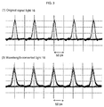
- Fig. 3 shows waveforms by actual wavelength conversion, in which Fig. 3(1) shows a waveform pattern of the original signal light 16 and Fig. 3(2) shows a waveform pattern of the converted light 18. It is known that the data pattern of the 1,552 nm light (original signal light 16) having the waveform of ultrashort optical pulses of approximately 10 ps is faithfully copied to the converted light 18 of the wavelength 1,560 nm. Also, an acceptable extinction ratio is obtained.
- any other absorptive optical modulator can be used provided that it can forcibly discharge electrons and/or holes produced in the optical modulator by absorption to external circuit prior to thermal diffusion by using an electric field generated in the optical modulator by a voltage applied to the optical modulator.
- a waveguide-type MQW optical modulator using quantum Stark effect of multiquantum wells (MQW) of semiconductors can be used.
- the wavelength-converted light 18 has the form of wavelength-division multiplexed light of optical signals of different wavelengths contained in the probe light 12 and having the same data pattern as that of the original signal light 16. For all wavelengths, acceptable waveforms could be obtained.
- the embodiment is configured that the probe light 12 and the original signal light 16 travel in the opposite directions within the optical modulator 10. Also when they travel in the same direction, similar wavelength conversion is attained. However, a pattern effect appears in the wavelength-converted light, depending on characteristics of the absorptive optical modulator, and it is difficult to obtain acceptable waveforms as shown in Fig. 3.
- a transmission-type electroabsorption optical modulator a different optical modulator can be used. For example, by using a reflective electroabsorption optical modulator having one end surface with a higher reflectance than the other and by making the original signal light and the probe light to travel in opposite directions in the optical modulator, similar effects can be obtained due to mutual absorption saturation characteristics between the original signal light and the probe light.
- the embodiment can use any typical electroabsorption optical modulator in its original form. Basically, therefore, it need not use elements with complicated structures or special semiconductor crystals. As a result, simple, high-quality, highly-reliable and inexpensive wavelength converters and optically operational devices can be realized. Moreover, since the embodiment is configured to once convert the original signal light to electron-hole pairs and then convert its optical intensity information alone to wavelength-converted light, it results in the additional advantage that optical phase distortion contained in the original signal is not converted to wavelength-converted light.
- the embodiment uses the optical circulator 14 to feed the original signal light 16 to the end surface 10b of the optical modulator 10 and to take out the data-modulated probe light emitted from the end surface 10b.
- the same function can be realized by using another appropriate dividing/multiplexing device such as WDM coupler or 3 dB coupler. That is, any optical element may be used, which can feed the externally introduced original signal light 16 to the end surface 10b of the optical modulator 10 and can take out the wavelength-converted light 18 output from the end surface 10b separately from the original signal light 16.
- the embodiment has been illustrated as using a DC voltage as the voltage applied to the optical modulator 10.
- a DC voltage as the voltage applied to the optical modulator 10.
- by superposing signals on the applied voltage it is possible to superpose system monitoring signals on the converted light 18 and to add a sampling function, waveform-shaping function and noise-suppressing function as explained later.
- the signal modifies the absorptive characteristics of the optical modulator 10, and therefore the extinction ratio of the wavelength-converted light 18 is further improved.
- Absorption wavelength characteristics of electroabsorption optical modulators in general, can be controlled by changing their temperatures. Therefore, also the embodiment shown in Fig. 1 can realize satisfactory waveform-conversion characteristics over a wide wavelength range by appropriately controlling the temperature of the optical modulator 10 by the electronic cooling device 11.
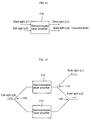
- Fig. 4 is a schematic block diagram showing a general construction of a modified version of the embodiment shown in Fig. 1. This arrangement inserts two optical circulators 20, 22 and optical amplifier 24 between the optical modulator 10 and the optical circulator 14 to selectively amplify output light of the probe light 12 data-modulated in the optical modulator 10 and output from it.
- the end surface 10b of the optical modulator 10 is connected to terminal B of the optical circulator 20, and terminal C of the optical circulator 20 is connected to the input of the optical amplifier 24.
- Output of the optical amplifier 24 is connected to terminal A of the optical circulator 14
- terminal B of the optical circulator 22 is connected to terminal B of the optical circulator 14
- terminal C of the optical circulator 22 is connected to terminal A of the optical circulator 20.
- the original signal light 16 is fed to terminal A of the optical circulator 14, next from terminal B thereof to terminal B of the optical circulator 22, next from terminal C of the optical circulator 22 to terminal A of the optical circulator 20, and further from terminal B of the optical circulator 20 to the end surface 10b of the optical modulator 10.
- the probe light 12 which is continuous light like that of the embodiment shown in fig. 1.
- the optical modulator 10 attenuates the probe light 12 in accordance with the original signal light 16 from the end surface 10b.
- the probe light 12 having the same aspect of changes in intensity as that of the original signal light 16, namely the wavelength-converted light 18, is output from the end surface 10b to the terminal B of the optical circulator 20.
- the wavelength-converted light 18 input to the terminal B of the optical circulator 20 is supplied from the terminal C to the optical amplifier 24, optically amplified there, and applied to the terminal A of the optical circulator 22.
- the light input to the terminal A of the optical circulator 22 is delivered from the terminal B to the terminal B of the optical circulator 14, and output from the terminal C of the optical circulator 14.
- the wavelength-converted light 18 after wavelength conversion by the optical modulator 12 is optically amplified by the optical amplifier 24, and then supplied to the next stage.
- the wavelength-converted light 18 is amplified by the optical amplifier 24, even when the original signal light 16 input to the terminal A of optical circulator 14 leaks to the terminal C, the leak component of the original signal light 16 need not be removed from output light at the terminal C of the optical circulator 14 and it is possible to reduce signal deterioration of the wavelength-converted light 18 caused by cross-talk.
- the wavelength-converted light 18 is optically amplified by the optical amplifier 24.
- an additional optical amplifier may be provided between the terminal C of the optical circulator 22 and the terminal A of the optical circulator 20 to optically amplify the original signal light 16 appropriately.
- the probe light 12 need not be CW light. If the probe light 12 is modulated, for example, the wavelength-converted light 18 has the waveform resulting from intensity modulation of the probe light 12 by the waveform of the original signal light 16. That is, the waveform of the wavelength-converted light 18 corresponds to one obtained by multiplying (logic product) the original signal light 16 and the probe light 12.
- the waveform of the wavelength-converted light 18 has a form obtained by sampling the original signal light 16 by the repetitive frequency f1. Even when the original signal light 16 contains noise light, the level of the noise light in the original signal light 16 is greatly suppressed in the wavelength-converted light 18. That is, waveform shaping function and noise suppressing function can be realized in the optical stage. This is derived from the use of the absorptive optical modulator 10 promising sufficiently large changes in absorption loss relative to the optical power of the original signal light as shown in Fig. 2.
- the voltage applied to the optical modulator 10 is a pulsating voltage such as probe light 12
- sampling and waveform-shaping of the original signal light 16 and suppression of noise can be attained similarly.
- modulation of the probe light 12 is more effective and convenient because, by increasing the input power of the probe light, the output power can be increased, and distortion in optical phase contained in the original signal light can be removed.
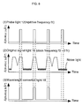
- Fig. 7 shows another when f0 ⁇ f1
- (1) is the waveform of the probe light 12
- (2) is the waveform of the original signal light 16
- (3) is the waveform of the wavelength-converted light 18.
- the waveform of the wavelength-converted light 18 varies depending on the relationship between the entry timing of the probe light 12 into the optical modulator 10 and the entry timing of the original signal light 16 into the optical modulator 10. Therefore, the entry timing of the probe signal 12 into the optical modulator 10 can be locked with the entry timing of the original signal light 16 into the optical modulator 10 by adjusting the entry timing of the probe light 12 into the optical modulator 10 by referring to the waveform of the wavelength-converted light 18, namely the average intensity (or peak intensity), so as to maximize the average intensity of the wavelength-converted light 18.
- f0 is not equal to f1 (Figs.
- the waveform of the wavelength-converted light 18 may be regarded as having been intensity-modulated at the differential frequency between f0 and f1.
- an optical PLL (phase-locked loop) circuit can be made by detecting the average level of the wavelength-converted light 18 and by controlling the modulation frequency of the probe light 12 to maximize the detected level.
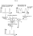
- Fig. 9 is a schematic block diagram showing a general construction of an optical PLL circuit made by using the embodiment shown in Fig. 1. Identical or equivalent elements are labelled with reference numerals common to those in Fig. 1.
- a photodetective element 30 converts the wavelength-converted light 18 into an electric signal
- an integrating circuit 32 integrates or smoothes the output of the photodetective element 30.
- a voltage controlled oscillator 34 oscillates in a frequency responsive to the output voltage of the integrating circuit 32, and its output is applied to a laser drive circuit 36.
- the laser drive circuit 36 drives a semiconductor laser 38 in the output frequency of the oscillator 34 (for example, pulse driving or sinusoidal modulation driving) to emit laser light of a desired waveform. Output light of the semiconductor laser 38 is used as the probe light 12 and applied to the optical modulator 10.
- an optical isolator 40 may be provided between the semiconductor laser 38 and the end surface 10a of the optical modulator 10 to absorb the original signal light 16, if any, output from the end surface 10a of the optical modulator 10.
- an optical filter is preferably provided just before the photodetective element 30 to remove or suppress any wavelength light other than the wavelength-converted light 18.
- a receiver circuit 42 demodulates data from output signals of the photodetective element 30 in accordance with the output clock of the voltage controlled oscillator 34.
- the wavelength-converted light 18 is light obtained by decoding the data signal transported by the original signal light 16 and suppressing the accumulated noise. This is because respective pulse waveforms of the wavelength-converted light 18 depend on respective pulse waveforms of the probe light 12.
- the embodiment shown in Fig. 9 has both a waveform-shaping function and a noise suppressing function.
- the probe light 12 is in form of a repeat RZ signal.
- a cosine-square waveform or any other modulated waveform such as data-modulated RZ- or NRZ-modulated light, is acceptable for optical PLL.
- the waveform of the wavelength-converted light 18 is one obtained by dividing the original signal light 16 on the time base. That is, the time-division multiplexed optical signal can be demultiplexed on the time base in the form of optical signal.
- the electroabsorption optical modulator 10 changes in absorptive characteristics with applied voltage. While the applied voltage is low, the absorption loss of the probe light exhibits relatively flat changes with power change of the original signal light. However, when the applied voltage is high, the absorption loss of the probe light exhibits relatively keen changes with power change of the original signal light.
- the time-base division function of the time-division multiplexed optical signal can be increased by adjusting the applied voltage of the optical modulator 10 in synchronism with the repetitive frequency of the probe light 12. In short, noise can be suppressed significantly.
- the applied voltage of the optical modulator 10 is in synchronism with the frequency f0/2 of the probe light 12.
- the applied voltage of the optical modulator 10 is controlled to be low voltage when the intensity of the probe light 12 is a high level.
- the waveform of the wavelength-converted light 18 results in a form obtained by sampling the original signal light 16 in the half frequency thereof and largely suppressing the noise light.
- this embodiment uses a sinusoidal wave as the applied voltage
- any desired modulated waveform such as cosine-square waveform or RZ pulse waveform, may be superposed or added to the applied voltage in order to obtain a desired effect.
- the embodiment can realize not only wavelength conversion but also waveform shaping and noise suppression.
- the embodiment is also applicable to cross-connected optical systems.
- wavelength is converted and the large extinction ratio is obtained, using very simple construction.
- the invention promises effective improvements in signal quality.
- the invention can realize economical, high-performance wavelength converters, waveform converters and optical PLL circuits, and can greatly contribute to developments of optical transmission systems.
Applications Claiming Priority (3)
| Application Number | Priority Date | Filing Date | Title |
|---|---|---|---|
| JP233796/96 | 1996-09-04 | ||
| JP23379696A JP3458613B2 (ja) | 1996-09-04 | 1996-09-04 | 波長変換装置及び光演算装置 |
| JP962337/96 | 1996-09-04 |
Publications (2)
| Publication Number | Publication Date |
|---|---|
| EP0828174A2 true EP0828174A2 (fr) | 1998-03-11 |
| EP0828174A3 EP0828174A3 (fr) | 1998-11-25 |
Family
ID=16960714
Family Applications (1)
| Application Number | Title | Priority Date | Filing Date |
|---|---|---|---|
| EP97114500A Withdrawn EP0828174A3 (fr) | 1996-09-04 | 1997-08-21 | Dispositif de conversion de longueur d'onde optique et circuit de détection de phase d'impulsions optiques |
Country Status (3)
| Country | Link |
|---|---|
| US (1) | US5959764A (fr) |
| EP (1) | EP0828174A3 (fr) |
| JP (1) | JP3458613B2 (fr) |
Cited By (7)
| Publication number | Priority date | Publication date | Assignee | Title |
|---|---|---|---|---|
| EP1113596A2 (fr) * | 1999-12-27 | 2001-07-04 | DDI Corporation | Formeur d'onde optique |
| EP1128593A2 (fr) * | 2000-02-28 | 2001-08-29 | Mitsubishi Denki Kabushiki Kaisha | Récepteur optique |
| EP1137213A2 (fr) * | 2000-03-24 | 2001-09-26 | DDI Corporation | Multiplexeur optique de TDM, démultiplexeur optique de TDM , convertisseur WDM/TDM et convertisseur TDM/WDM |
| EP1193894A2 (fr) * | 2000-09-29 | 2002-04-03 | KDD Submarine Cable Systems Inc. | Générateur d'impulsions optiques à bande étroite |
| EP1973246A1 (fr) | 2007-03-20 | 2008-09-24 | Fujitsu Limited | Appareil de contrôle de forme d'onde optique |
| US9976919B2 (en) | 2015-03-27 | 2018-05-22 | Kettering University | Fiber-optic sensor assembly |
| US20210273407A1 (en) * | 2018-09-21 | 2021-09-02 | Hamamatsu Photonics K.K. | Laser device, and laser waveform control method |
Families Citing this family (25)
| Publication number | Priority date | Publication date | Assignee | Title |
|---|---|---|---|---|
| FR2757719B1 (fr) * | 1996-12-19 | 1999-01-22 | Alsthom Cge Alcatel | Repeteur pour systeme de transmission a fibre optique a signaux solitons |
| FR2758669B1 (fr) * | 1997-01-23 | 1999-02-19 | Alsthom Cge Alcatel | Procede de modulation et modulateur optique a semi conducteur |
| JP3438770B2 (ja) * | 1998-03-06 | 2003-08-18 | Kddi株式会社 | 光ディジタル再生装置 |
| US6335819B1 (en) | 1999-02-19 | 2002-01-01 | University Of Maryland | All-optical regeneration at high bit rates using an electroabsorption modulator |
| JP2001024585A (ja) * | 1999-07-02 | 2001-01-26 | Kdd Corp | 光受信装置及び光アド/ドロップ装置 |
| JP2001147409A (ja) | 1999-11-19 | 2001-05-29 | Ddi Corp | 光信号処理装置 |
| US6426831B1 (en) | 2000-02-29 | 2002-07-30 | Massachusetts Institute Of Technology | EIT based optical switch/wavelength converter |
| JP2001264712A (ja) * | 2000-03-16 | 2001-09-26 | Japan Science & Technology Corp | 全光制御システム |
| US6624922B1 (en) * | 2000-06-02 | 2003-09-23 | Northrop Grumman Corporation | Electro-optic device for adding/subtracting optical signals |
| US20020085266A1 (en) * | 2000-11-27 | 2002-07-04 | Yao Xiaotian Steve | Wavelength converter with an impedance matched electro-absorption modulator pair |
| US6710911B2 (en) | 2001-03-02 | 2004-03-23 | Evident Technologies | Optical wavelength converter |
| JP2003005140A (ja) * | 2001-06-19 | 2003-01-08 | Kddi Corp | 光信号再生装置 |
| US7072393B2 (en) | 2001-06-25 | 2006-07-04 | International Business Machines Corporation | Multiple parallel encoders and statistical analysis thereof for encoding a video sequence |
| JP4540886B2 (ja) | 2001-06-29 | 2010-09-08 | 富士通株式会社 | 光信号の波形を整形する方法及び装置 |
| US6888666B1 (en) * | 2001-11-16 | 2005-05-03 | Dakota Investment Group, Inc. | Dynamically reconfigurable optical amplification element |
| US6856441B2 (en) * | 2002-08-23 | 2005-02-15 | T-Networks, Inc. | Method of tuning wavelength tunable electro-absorption modulators |
| JP2004219447A (ja) | 2003-01-09 | 2004-08-05 | Mitsubishi Electric Corp | 波長変換器 |
| US20050018271A1 (en) | 2003-03-26 | 2005-01-27 | Kddi R&D Laboratories Inc. | Apparatus for simultaneous OTDM demultiplexing, electrical clock recovery and optical clock generation, and optical clock recovery |
| JP3815453B2 (ja) * | 2003-03-27 | 2006-08-30 | Kddi株式会社 | 光信号処理装置及び方法 |
| JP3762997B2 (ja) * | 2003-08-28 | 2006-04-05 | 独立行政法人情報通信研究機構 | 光パルス分離装置及び方法 |
| ITMI20042312A1 (it) * | 2004-12-01 | 2005-03-01 | Marconi Comm Spa | Multiplexer con add-drop ottico |
| US7623798B1 (en) * | 2005-10-04 | 2009-11-24 | Sprint Communications Company L.P. | Polarization mode dispersion mitigation of multiple optical communication channels |
| US7782913B2 (en) * | 2007-07-20 | 2010-08-24 | Corning Incorporated | Intensity modulation in wavelength converting optical package |
| US9634767B2 (en) * | 2012-12-10 | 2017-04-25 | Telefonaktiebolaget Lm Ericsson (Publ) | Power control in bidirectional WDM optical link |
| JP6128134B2 (ja) | 2013-01-21 | 2017-05-17 | 富士通株式会社 | 周波数変換装置、波長多重装置および周波数変換方法 |
Citations (6)
| Publication number | Priority date | Publication date | Assignee | Title |
|---|---|---|---|---|
| EP0275554A2 (fr) * | 1987-01-19 | 1988-07-27 | Hitachi, Ltd. | Dispositif optique |
| US5080504A (en) * | 1990-06-28 | 1992-01-14 | Varian Associates, Inc. | Optical switching apparatus and method |
| JPH05259581A (ja) * | 1992-03-16 | 1993-10-08 | Nippon Telegr & Teleph Corp <Ntt> | 波長変換器 |
| US5289489A (en) * | 1991-02-28 | 1994-02-22 | Canon Kabushiki Kaisha | All-optical light modulating apparatus and all-optical process for modulating light |
| JPH08220494A (ja) * | 1995-02-15 | 1996-08-30 | Nippon Telegr & Teleph Corp <Ntt> | 偏波無依存光位相同期ループ回路 |
| DE19535772A1 (de) * | 1995-09-26 | 1997-03-27 | Siemens Ag | Optische Konversion der Trägerwellenlänge optisch übertragener Datensignale |
Family Cites Families (5)
| Publication number | Priority date | Publication date | Assignee | Title |
|---|---|---|---|---|
| US4818898A (en) * | 1986-09-10 | 1989-04-04 | E. I. Du Pont De Nemours And Company | Optical nonlinearity in organic and organometallic molecules via lattice inclusion complexation |
| JP3151881B2 (ja) * | 1991-06-07 | 2001-04-03 | キヤノン株式会社 | 光パルス幅測定装置 |
| US5165105A (en) * | 1991-08-02 | 1992-11-17 | Minnesota Minning And Manufacturing Company | Separate confinement electroabsorption modulator utilizing the Franz-Keldysh effect |
| US5402259A (en) * | 1993-04-23 | 1995-03-28 | Trw Inc. | Linear electroabsorptive modulator and related method of analog modulation of an optical carrier |
| US5784188A (en) * | 1996-02-13 | 1998-07-21 | Matsushita Electric Industrial Co., Inc. | Electro-absorption optical modulator and method for fabricating the same |
-
1996
- 1996-09-04 JP JP23379696A patent/JP3458613B2/ja not_active Expired - Fee Related
-
1997
- 1997-08-21 EP EP97114500A patent/EP0828174A3/fr not_active Withdrawn
- 1997-09-04 US US08/923,349 patent/US5959764A/en not_active Expired - Fee Related
Patent Citations (6)
| Publication number | Priority date | Publication date | Assignee | Title |
|---|---|---|---|---|
| EP0275554A2 (fr) * | 1987-01-19 | 1988-07-27 | Hitachi, Ltd. | Dispositif optique |
| US5080504A (en) * | 1990-06-28 | 1992-01-14 | Varian Associates, Inc. | Optical switching apparatus and method |
| US5289489A (en) * | 1991-02-28 | 1994-02-22 | Canon Kabushiki Kaisha | All-optical light modulating apparatus and all-optical process for modulating light |
| JPH05259581A (ja) * | 1992-03-16 | 1993-10-08 | Nippon Telegr & Teleph Corp <Ntt> | 波長変換器 |
| JPH08220494A (ja) * | 1995-02-15 | 1996-08-30 | Nippon Telegr & Teleph Corp <Ntt> | 偏波無依存光位相同期ループ回路 |
| DE19535772A1 (de) * | 1995-09-26 | 1997-03-27 | Siemens Ag | Optische Konversion der Trägerwellenlänge optisch übertragener Datensignale |
Non-Patent Citations (3)
| Title |
|---|
| PATENT ABSTRACTS OF JAPAN vol. 018, no. 022 (E-1490), 13 January 1994 -& JP 05 259581 A (NIPPON TELEGR & TELEPH CORP), 8 October 1993, * |
| PATENT ABSTRACTS OF JAPAN vol. 096, no. 012, 26 December 1996 -& JP 08 220494 A (NIPPON TELEGR &TELEPH CORP <NTT>), 30 August 1996, * |
| YOO S J B: "WAVELENGTH CONVERSION TECHNOLOGIES FOR WDM NETWORK APPLICATIONS" JOURNAL OF LIGHTWAVE TECHNOLOGY, vol. 14, no. 6, 1 June 1996, pages 955-966, XP000598499 * |
Cited By (13)
| Publication number | Priority date | Publication date | Assignee | Title |
|---|---|---|---|---|
| EP1113596A2 (fr) * | 1999-12-27 | 2001-07-04 | DDI Corporation | Formeur d'onde optique |
| EP1113596A3 (fr) * | 1999-12-27 | 2003-05-14 | DDI Corporation | Formeur d'onde optique |
| EP1128593A2 (fr) * | 2000-02-28 | 2001-08-29 | Mitsubishi Denki Kabushiki Kaisha | Récepteur optique |
| EP1128593A3 (fr) * | 2000-02-28 | 2006-06-14 | Mitsubishi Denki Kabushiki Kaisha | Récepteur optique |
| US6775478B2 (en) | 2000-03-24 | 2004-08-10 | Ddi Corporation | Optical TDM multiplexer, optical TDM demultiplexer, WDM/TDM converter and TDM/WDM converter |
| EP1137213A2 (fr) * | 2000-03-24 | 2001-09-26 | DDI Corporation | Multiplexeur optique de TDM, démultiplexeur optique de TDM , convertisseur WDM/TDM et convertisseur TDM/WDM |
| EP1137213A3 (fr) * | 2000-03-24 | 2002-12-18 | DDI Corporation | Multiplexeur optique de TDM, démultiplexeur optique de TDM , convertisseur WDM/TDM et convertisseur TDM/WDM |
| EP1193894A2 (fr) * | 2000-09-29 | 2002-04-03 | KDD Submarine Cable Systems Inc. | Générateur d'impulsions optiques à bande étroite |
| EP1193894A3 (fr) * | 2000-09-29 | 2002-11-20 | KDD Submarine Cable Systems Inc. | Générateur d'impulsions optiques à bande étroite |
| EP1973246A1 (fr) | 2007-03-20 | 2008-09-24 | Fujitsu Limited | Appareil de contrôle de forme d'onde optique |
| US8275264B2 (en) | 2007-03-20 | 2012-09-25 | Fujitsu Limited | Optical waveform controlling apparatus |
| US9976919B2 (en) | 2015-03-27 | 2018-05-22 | Kettering University | Fiber-optic sensor assembly |
| US20210273407A1 (en) * | 2018-09-21 | 2021-09-02 | Hamamatsu Photonics K.K. | Laser device, and laser waveform control method |
Also Published As
| Publication number | Publication date |
|---|---|
| US5959764A (en) | 1999-09-28 |
| JPH1078595A (ja) | 1998-03-24 |
| EP0828174A3 (fr) | 1998-11-25 |
| JP3458613B2 (ja) | 2003-10-20 |
Similar Documents
| Publication | Publication Date | Title |
|---|---|---|
| US5959764A (en) | Wavelength converter, optically operational device and optical pulse phase detecting circuit | |
| US9065243B2 (en) | Optical amplifier | |
| EP1079552B1 (fr) | Procédé, dispositif optique et système de transmission à fibres optiques | |
| Joergensen et al. | All-optical wavelength conversion at bit rates above 10 Gb/s using semiconductor optical amplifiers | |
| US7099586B2 (en) | Reconfigurable multi-channel all-optical regenerators | |
| US6963436B2 (en) | Method and device for waveform shaping of signal light | |
| US6335819B1 (en) | All-optical regeneration at high bit rates using an electroabsorption modulator | |
| US6778730B2 (en) | Optical signal processing device | |
| US6204944B1 (en) | All-optical time-division demultiplexing circuit and all-optical TDM-WDM conversion circuit | |
| JP2004037985A (ja) | 光andゲート及び波形成形装置 | |
| US6728019B2 (en) | Optical gate and optical phase modulator | |
| Connelly | Semiconductor optical amplifiers and their applications | |
| US7277222B2 (en) | Apparatus and method for wavelength conversion and clock signal extraction using semiconductor optical amplifiers | |
| Zoiros et al. | Semiconductor optical amplifier pattern effect suppression using a birefringent fiber loop | |
| US20070104492A1 (en) | System for and method of single slideband modulation for analog optical link | |
| EP1271810B1 (fr) | Procédé et dispositif de mise en forme d'onde d'un signal optique | |
| US20040109690A1 (en) | Optical control method and device | |
| US20030043431A1 (en) | Simultaneous demultiplexing and clock recovery of high-speed OTDM signals using a tandem electro-absorption modulator | |
| Kuwatsuka | Wavelength conversion technologies for photonic network systems | |
| Cho et al. | RZ wavelength conversion with reduced power penalty using a semiconductor-optical-amplifier/fiber-grating hybrid device | |
| Rau et al. | Simultaneous all-optical demultiplexing of a 40-Gb/s signal to 4 x 10 Gb/s WDM channel's using an ultrafast fiber wavelength converter | |
| Forsyth et al. | Semiconductor optical amplifiers: present and future applications | |
| US20030190167A1 (en) | All-optical regenerator for wavelength-division multiplexed signals | |
| Sabapathi et al. | Analysis of optical modulation formats for DWDM system | |
| Cho et al. | Wavelength conversion using a noninterferometric semiconductor-optical-amplifier/fiber-Bragg-grating device |
Legal Events
| Date | Code | Title | Description |
|---|---|---|---|
| PUAI | Public reference made under article 153(3) epc to a published international application that has entered the european phase |
Free format text: ORIGINAL CODE: 0009012 |
|
| AK | Designated contracting states |
Kind code of ref document: A2 Designated state(s): DE FR |
|
| AX | Request for extension of the european patent |
Free format text: AL;LT;LV;RO;SI |
|
| K1C1 | Correction of patent application (title page) published |
Effective date: 19980311 |
|
| PUAL | Search report despatched |
Free format text: ORIGINAL CODE: 0009013 |
|
| AK | Designated contracting states |
Kind code of ref document: A3 Designated state(s): AT BE CH DE DK ES FI FR GB GR IE IT LI LU MC NL PT SE |
|
| AX | Request for extension of the european patent |
Free format text: AL;LT;LV;RO;SI |
|
| 17P | Request for examination filed |
Effective date: 19981209 |
|
| AKX | Designation fees paid |
Free format text: DE FR |
|
| 17Q | First examination report despatched |
Effective date: 20020712 |
|
| STAA | Information on the status of an ep patent application or granted ep patent |
Free format text: STATUS: THE APPLICATION HAS BEEN WITHDRAWN |
|
| 18W | Application withdrawn |
Withdrawal date: 20021119 |