EP0827151B1 - Self cut-off type sense amplifier operable over a wide range of power supply voltages - Google Patents
Self cut-off type sense amplifier operable over a wide range of power supply voltages Download PDFInfo
- Publication number
- EP0827151B1 EP0827151B1 EP97114945A EP97114945A EP0827151B1 EP 0827151 B1 EP0827151 B1 EP 0827151B1 EP 97114945 A EP97114945 A EP 97114945A EP 97114945 A EP97114945 A EP 97114945A EP 0827151 B1 EP0827151 B1 EP 0827151B1
- Authority
- EP
- European Patent Office
- Prior art keywords
- circuit
- sense
- amplifier
- signal
- generating
- Prior art date
- Legal status (The legal status is an assumption and is not a legal conclusion. Google has not performed a legal analysis and makes no representation as to the accuracy of the status listed.)
- Expired - Lifetime
Links
- 238000001514 detection method Methods 0.000 claims description 39
- 230000000873 masking effect Effects 0.000 claims description 14
- 230000003213 activating effect Effects 0.000 claims description 7
- 230000005540 biological transmission Effects 0.000 claims description 2
- 230000004913 activation Effects 0.000 description 28
- 238000010586 diagram Methods 0.000 description 8
- 201000008103 leukocyte adhesion deficiency 3 Diseases 0.000 description 7
- 230000003247 decreasing effect Effects 0.000 description 6
- 230000000630 rising effect Effects 0.000 description 2
- 230000007704 transition Effects 0.000 description 2
- 230000000295 complement effect Effects 0.000 description 1
- 230000001934 delay Effects 0.000 description 1
- 230000004048 modification Effects 0.000 description 1
- 238000012986 modification Methods 0.000 description 1
- 230000003068 static effect Effects 0.000 description 1
Images


Classifications
-
- G—PHYSICS
- G11—INFORMATION STORAGE
- G11C—STATIC STORES
- G11C7/00—Arrangements for writing information into, or reading information out from, a digital store
- G11C7/06—Sense amplifiers; Associated circuits, e.g. timing or triggering circuits
-
- G—PHYSICS
- G11—INFORMATION STORAGE
- G11C—STATIC STORES
- G11C7/00—Arrangements for writing information into, or reading information out from, a digital store
- G11C7/22—Read-write [R-W] timing or clocking circuits; Read-write [R-W] control signal generators or management
-
- G—PHYSICS
- G11—INFORMATION STORAGE
- G11C—STATIC STORES
- G11C7/00—Arrangements for writing information into, or reading information out from, a digital store
- G11C7/06—Sense amplifiers; Associated circuits, e.g. timing or triggering circuits
- G11C7/062—Differential amplifiers of non-latching type, e.g. comparators, long-tailed pairs
-
- G—PHYSICS
- G11—INFORMATION STORAGE
- G11C—STATIC STORES
- G11C2207/00—Indexing scheme relating to arrangements for writing information into, or reading information out from, a digital store
- G11C2207/06—Sense amplifier related aspects
- G11C2207/065—Sense amplifier drivers
Definitions
- the present invention relates to a sense amplifier, and more particularly, to a self cut-off type sense amplifier for a static random access memory (SRAM) device.
- SRAM static random access memory
- an SRAM device after a precharging operation is carried out, complementary data is read from a selected memory cell and is sensed by a sense amplifier.
- the power dissipation of SRAM devices is mainly determined by the precharging operation and the operation of the sense amplifier.
- a prior art self cut-off type sense amplifier includes an amplifier circuit for amplifying a difference in potential between first and second data lines, an amplifier circuit activating circuit for receiving a sense start signal to activate the amplifier circuit and receiving a sense end signal to deactivate the amplifier circuit, a first sense detecting circuit for determining whether or not the amplifier circuit is activated in accordance with a first output voltage thereof and generating a first sense detection signal, a second sense detecting circuit for determining whether or not the amplifier circuit is activated in accordance with a second output voltage thereof and generating a second sense detection signal, and a sense end signal generating circuit for receiving at least one of the first and second sense detection signals and generating the sense end signal when a predetermined time has passed after at least one of the first and second sense detection signals is received.
- a self cut-off type sense amplifier which includes an amplifier circuit for amplifying a difference in potential between first and second data lines, an amplifier circuit activating circuit for receiving a sense start signal to activate the amplifier circuit and receiving a sense end signal to deactivate the amplifier circuit, a first sense detecting circuit for determining whether or not the amplifier circuit is activated in accordance with a first output voltage thereof and generating a first sense detection signal, a second sense detecting circuit for determining whether or not the amplifier circuit is activated in accordance with a second output voltage thereof and generating a second sense detection signal, and a sense end signal generating circuit for receiving at least one of the first and second sense detection signals and generating the sense end signal when a predetermined time has passed after the at least one of the first and second sense detection signals is received, a masking circuit is connected between the first and second sense detecting circuits and the sense end signal generating circuit, and prohibits transmission of the first and second sense detection signals to the sense end signal generating circuit only when the first and second sense detection
- the masking circuit delays the sense end signal, so that the timing of deactivating the amplifier circuit is after the timing of establishing output data.
- reference numeral 1 designates a memory cell array including memory cells (not shown) at intersections between word lines such as WL 1 and bit line pairs such as BL 1 and BL 1 .
- an address buffer 2 receives an external address ADD and generates an internal address IADD.
- An X component of the internal address IADD is supplied to a row decoder 3 for selecting one of the word lines, and a Y component of the internal address IADD is supplied to a column decoder 4, so that a column selector 5 selects one pair of the bit line pairs.
- a column decoder 4 selects one pair of the bit line pairs.
- the internal address IADD is supplied to an address transition detection (ATD) circuit 6 for detecting a transition of the internal address IADD to generate an ATD signal ⁇ ATD .
- ATD address transition detection
- a control circuit 7 receives the ATD signal ⁇ ATD as well as an inverted signal of a write enable signal WE to generate a precharging signal ⁇ PR , a sense activation signal ⁇ S and a write activation signal ⁇ W .
- the precharging signal ⁇ PR is supplied to precharging transistors connected to the bit lines, thus precharging the bit lines.
- the sense activation signal ⁇ S is supplied as a sense start signal to a sense amplifier 8, thus activating the sense amplifier 8.
- the write activation signal ⁇ W is supplied to a write amplifier 9, thus activating the write amplifier 9.
- the precharging signal ⁇ PR is generated from the control circuit 7 in synchronization with the ATD signal ⁇ ATD , and thereafter, one memory cell is selected by the row decoder 3 and the column decoder 4 using the internal address IADD.
- the write amplifier circuit 9 is activated, so that potentials at data lines D and D are changed in accordance with input data DI, and the potentials are written into the selected memory cell.
- the precharging signal ⁇ PR is also generated from the control circuit 7 in synchronization with the ATD signal ⁇ ATD , and thereafter, one memory cell is selected by the row decoder 3 and the column decoder 4 using the internal address IADD. As a result, potentials at the data lines D and D are changed in accordance with data in the selected memory cell. In this state, since the sense activation signal ⁇ S is also generated from the control circuit 7, the sense amplifier 8 is activated, so that the potentials at the data lines D and D are amplified, thus obtaining output data DO.
- Fig. 2 which is a detailed circuit diagram of the sense amplifier of Fig. 1, two stages of amplifier circuits 81 and 82, a sense detection circuit 83, a sense end signal generating circuit 84, and an internal sense activation signal generating circuit 85 for activating and deactivating the sense amplifier circuits 81 and 82 are provided.
- the amplifier circuit 81 is of a two end type which amplifies the potentials at the data lines D and D and generates potentials at data lines DOI and DOI .
- the amplifier circuit 81 is formed by a current mirror circuit 811 for receiving the potentials at the data lines D and D , a current mirror circuit 812 for receiving the potentials at the data lines D and D, an N-channel MOS transistor 813 for turning ON and OFF the current mirror circuits 811 and 812, and a P-channel MOS transistor 814 for equalizing the potentials at the data lines D and D .
- the amplifier circuit 82 is of a single end type which amplifies the potentials at the data lines DOI and DOI and generates the output data DO.
- the amplifier circuit 82 is formed by a current mirror circuit 821 for receiving the potentials at the data lines DOI and DOI , an N-channel MOS transistor 822 for turning ON and OFF the current mirror circuit 821, and P-channel MOS transistors 823 and 824 for pulling up the potentials at the data lines DOI and DOI .
- the sense detection circuit 83 is formed by inverters 831 and 832 for receiving the potentials at the data lines DOI and DOI , respectively.
- the inverters 831 and 832 have a common threshold voltage V th which is, in this case, an operating point. If the potential of the DOI is lower than the operating point V th , the inverter 831 generates a sense detection signal N having a high potential. Similarly, if the potential of the DOI is lower than the operating point V th , the inverter 832 generates a sense detection signal N having a high potential.
- the sense end signal generating circuit 84 is formed by delay circuits 841 and 842 connected to the inverters 831 and 832, respectively, a NAND circuit 843 for receiving the sense detection signal N of the inverter 831 and the output of the delay circuit 841, and a NAND circuit 844 for receiving the output potential N of the inverter 832 and the output of the delay circuit 842. Also, a NAND circuit 845 is connected to the outputs of the NAND circuits 843 and 845, for generating a sense end signal SE.
- the sense activation signal generating circuit 85 generates an internal sense activation signal ⁇ SI . That is, the sense activation signal generating circuit 838 includes an RS flip-flop which is set by a rising edge of the sense activation signal ⁇ S and is reset by a rising edge of the sense end signal SE.
- the transistors 813 and 814 of the amplifier circuit 81 and the transistors 822, 823 and 824 of the amplifier circuit 82 are controlled by the internal sense activation signal ⁇ SI .
- the amplifiers 81 and 82 are turned ON and OFF by the internal sense activation signal ⁇ SI , so that the sense amplifier 8 is called a self-cut type sense amplifier.
- a power supply voltage V CC applied to the sense amplifier 8 is high, for example, 2.5 to 5.5V.
- the-sense activation signal ⁇ S is changed from low to high.
- the internal sense activation signal generating circuit 838 is set, so that the internal sense activation signal ⁇ SI rises at time t2.
- the amplifier circuits 81 and 82 are both activated.
- the amplifier circuit 81 since the current mirror circuits 811 and 812 are cross-coupled, although the potential at one of the data lines such as D remain at a high level, the potential at the other data line such as D is gradually decreased.
- the amplifier circuit 82 the potential at the data lines DOI and DOI are both gradually decreased, but the potential at one of the bit lines such as DOI is again increased.
- the NAND circuits 843, 844 and 845 in combination generate a tigger signal SE. That is, in Fig. 3, at time t3, the potential at the data line DOI becomes lower than the operating point V th , so that the sense detection signal N of the inverter 831 rises. Therefore, at time t4, when a time d corresponding to the delay time of the delay circuit 841 has passed, the sense end signal SE rises to reset the internal sense activation signal generating circuit 85, and accordingly, the internal sense activation signal ⁇ SI falls to deactivate the amplifiers 81 and 82.
- the sense activation signal ⁇ S is changed from low to high.
- the internal sense activation signal generating circuit 85 is set, so that the internal sense activation signal ⁇ SI rises at time t2.
- the amplifier circuits 81 and 82 are both activated.
- the potential at one of the data lines such as D remains at a high level, the potential at the other data line such as D is gradually decreased.
- the potentials at the data lines DOI and DOI are both gradually decreased, but the potential at one of the bit lines such as DOI is again increased.
- a masking circuit 86 is interposed between the sense detection circuit 83 and the sense and signal generating circuit 84 of Fig. 2. That is, when the inverters 831 and 832 simultaneously generate the sense detection signals N and N , the masking circuit 86 disables the sense detection signal N and N, so that the sense end signal generating circuit 84 is not operated.
- the masking circuit 86 is formed by a NOR circuit 861 connected to the data lines DOI and DOI for generating a mask signal MSK.
- the NOR circuit 861 has the same operating point V th as that of the inverters 831 and 832. Therefore, only when the potentials at the data lines DOI and DOI are both lower than the operating point V th , is the mask signal MSK made high.
- the masking circuit 86 is formed by two inverters 862 and 863 connected to the inverters 831 and 832, a NOR circuit 864 connected to the NOR circuit 861 and the inverter 862, and a NOR circuit 865 connected to the NOR circuit 861 and the inverter 863.
- the sense activation signal ⁇ S is changed from low to high.
- the internal sense activation signal generating circuit 85 is set, so that the internal sense activation signal ⁇ SI rises at time t2.
- the amplifier circuits 81 and 82 are both activated.
- the potential at one of the data lines such as D remains at a high level, the potential at the other data line such as D is gradually decreased.
- the potentials at the data lines DOI and DOI are both gradually decreased, but the potential at one of the bit lines such as DOI is again increased.
- the mask signal MSK is made low.
- the sense detection signals N and N and the outputs A and A of the inverters 862 and 863 are also changed.
- the sense end signal SE rises to reset the internal sense activation signal generating circuit 85, and accordingly, the internal sense activation signal ⁇ SI falls to deactivate the amplifiers 81 and 82.
- the avove-mentioned delay time of the delay circuits 841 and 842 is about 1 to 2 ns.
- the masking circuit 86 of Fig. 5 is modified into a masking circuit 86'.
- the masking circuit 86' is formed by a NAND circuit 861', a NAND circuit 862' and an inverter 863' serving as an AND circuit, a NAND circuit 864' and an inverter 865' serving as an AND circuit, and delay circuits 866' and 867'. NOte that the delay circuits 866' and 867' have a delay time which is approximately the same as the operation time of the NAND circuit 861'. Even in Fig.
- the NAND circuit 861' when the sense detection signals N and N are both high, the NAND circuit 861' generates a mask signal MSK, so that the outputs N1 and N1 of the inverters 863' and 865' are made low regardless of the sense detection signals N and N .
- the sense amplifier 8 of Fig. 7 operates in the same way as the sense amplifier 8 of Fig. 5.
- the present invention can be applied to a sense amplifier including a single differential amplifier as illustrated in Fig. 8, where the amplifier 82 is connected directly to the data lines DO and DO .
- the timing of an output data can be sufficiently before the cut off timing of the sense amplifier.
- normal output data can be obtained.
Description
- The present invention relates to a sense amplifier, and more particularly, to a self cut-off type sense amplifier for a static random access memory (SRAM) device.
- Generally, in an SRAM device, after a precharging operation is carried out, complementary data is read from a selected memory cell and is sensed by a sense amplifier. The power dissipation of SRAM devices is mainly determined by the precharging operation and the operation of the sense amplifier.
- In order to reduce the power dissipation by the operation of the sense amplifier, self cut-off type sense amplifiers have been developed, see US-A-5479374.
- A prior art self cut-off type sense amplifier includes an amplifier circuit for amplifying a difference in potential between first and second data lines, an amplifier circuit activating circuit for receiving a sense start signal to activate the amplifier circuit and receiving a sense end signal to deactivate the amplifier circuit, a first sense detecting circuit for determining whether or not the amplifier circuit is activated in accordance with a first output voltage thereof and generating a first sense detection signal, a second sense detecting circuit for determining whether or not the amplifier circuit is activated in accordance with a second output voltage thereof and generating a second sense detection signal, and a sense end signal generating circuit for receiving at least one of the first and second sense detection signals and generating the sense end signal when a predetermined time has passed after at least one of the first and second sense detection signals is received. Thus, since the amplifier circuit is automatically deactivated after a read operation is completed, the power dissipation can be reduced. This will be explained later in detail.
- In the above-mentioned prior art self cut-off sense amplifier, however, when a power supply voltage applied to the sense amplifier is reduced, the timing of deactivating the amplifier circuit is advanced, and at worst, the amplifier circuit is deactivated before output data is established. Also, this means that the power supply voltage of SRAM devices having such a self cut-off type sense amplifier is limited.
- It is an object of the present invention to provide a self cut-off sense amplifier operable over a wide range of power supply voltages.
- According to the present invention, in a self cut-off type sense amplifier which includes an amplifier circuit for amplifying a difference in potential between first and second data lines, an amplifier circuit activating circuit for receiving a sense start signal to activate the amplifier circuit and receiving a sense end signal to deactivate the amplifier circuit, a first sense detecting circuit for determining whether or not the amplifier circuit is activated in accordance with a first output voltage thereof and generating a first sense detection signal, a second sense detecting circuit for determining whether or not the amplifier circuit is activated in accordance with a second output voltage thereof and generating a second sense detection signal, and a sense end signal generating circuit for receiving at least one of the first and second sense detection signals and generating the sense end signal when a predetermined time has passed after the at least one of the first and second sense detection signals is received, a masking circuit is connected between the first and second sense detecting circuits and the sense end signal generating circuit, and prohibits transmission of the first and second sense detection signals to the sense end signal generating circuit only when the first and second sense detection signals are both generated.
- Thus, when the power supply voltage is reduced, the masking circuit delays the sense end signal, so that the timing of deactivating the amplifier circuit is after the timing of establishing output data.
- The present invention will be more clearly understood from the description as set forth below, in comparison with the prior art, with reference to the accompanying drawings, wherein:
- Fig. 1 is a block circuit diagram illustrating a prior art SRAM device;
- Fig. 2 is a detailed circuit diagram of the sense amplifier of Fig. 1;
- Figs. 3 and 4 are timing diagrams showing the operation of the sense amplifier of Fig. 2;
- Fig. 5 is a circuit diagram illustrating a first embodiment of the sense amplifier according to the present invention;
- Fig. 6 is a timing diagram showing the operation of the sense amplifier of Fig. 6;
- Fig. 7 is a circuit diagram illustrating a second embodiment of the sense amplifier according to the present invention; and
- Fig. 8 is a circuit diagram illustrating a modification of the sense amplifier of Fig. 5.
-
- Before the description of the preferred embodiments, a prior art sense amplifier will be explained with reference to Figs. 1, 2, 3 and 4.
- In Fig. 1, which illustrates a prior art SRAM device,
reference numeral 1 designates a memory cell array including memory cells (not shown) at intersections between word lines such as WL1 and bit line pairs such as BL1 andBL1 . Also, anaddress buffer 2 receives an external address ADD and generates an internal address IADD. An X component of the internal address IADD is supplied to a row decoder 3 for selecting one of the word lines, and a Y component of the internal address IADD is supplied to acolumn decoder 4, so that acolumn selector 5 selects one pair of the bit line pairs. Thus, one memory cell is accessed. - Further, the internal address IADD is supplied to an address transition detection (ATD)
circuit 6 for detecting a transition of the internal address IADD to generate an ATD signal ATD. - A
control circuit 7 receives the ATD signal ATD as well as an inverted signal of a write enable signal WE to generate a precharging signal PR, a sense activation signal S and a write activation signal W. Note that the precharging signal PR is supplied to precharging transistors connected to the bit lines, thus precharging the bit lines. Also, the sense activation signal S is supplied as a sense start signal to asense amplifier 8, thus activating thesense amplifier 8. Further, the write activation signal W is supplied to a write amplifier 9, thus activating the write amplifier 9. - In a write mode (
WE = "0"), the precharging signal PR is generated from thecontrol circuit 7 in synchronization with the ATD signal ATD, and thereafter, one memory cell is selected by the row decoder 3 and thecolumn decoder 4 using the internal address IADD. In this state, since the write activation signal W is also generated from thecontrol circuit 7, the write amplifier circuit 9 is activated, so that potentials at data lines D andD are changed in accordance with input data DI, and the potentials are written into the selected memory cell. - On the other hand, in a read mode (
WE = "1"), the precharging signal PR is also generated from thecontrol circuit 7 in synchronization with the ATD signal ATD, and thereafter, one memory cell is selected by the row decoder 3 and thecolumn decoder 4 using the internal address IADD. As a result, potentials at the data lines D andD are changed in accordance with data in the selected memory cell. In this state, since the sense activation signal S is also generated from thecontrol circuit 7, thesense amplifier 8 is activated, so that the potentials at the data lines D andD are amplified, thus obtaining output data DO. - In Fig. 2, which is a detailed circuit diagram of the sense amplifier of Fig. 1, two stages of
amplifier circuits sense detection circuit 83, a sense endsignal generating circuit 84, and an internal sense activationsignal generating circuit 85 for activating and deactivating thesense amplifier circuits - The
amplifier circuit 81 is of a two end type which amplifies the potentials at the data lines D andD and generates potentials at data lines DOI andDOI . In more detail, theamplifier circuit 81 is formed by acurrent mirror circuit 811 for receiving the potentials at the data lines D andD , acurrent mirror circuit 812 for receiving the potentials at the data linesD and D, an N-channel MOS transistor 813 for turning ON and OFF thecurrent mirror circuits channel MOS transistor 814 for equalizing the potentials at the data lines D andD . - The
amplifier circuit 82 is of a single end type which amplifies the potentials at the data lines DOI andDOI and generates the output data DO. In more detail, theamplifier circuit 82 is formed by acurrent mirror circuit 821 for receiving the potentials at the data lines DOI andDOI , an N-channel MOS transistor 822 for turning ON and OFF thecurrent mirror circuit 821, and P-channel MOS transistors DOI . - The
sense detection circuit 83 is formed byinverters DOI , respectively. Theinverters inverter 831 generates a sense detection signal N having a high potential. Similarly, if the potential of the DOI is lower than the operating point Vth, theinverter 832 generates a sense detection signalN having a high potential. - The sense end
signal generating circuit 84 is formed bydelay circuits inverters NAND circuit 843 for receiving the sense detection signal N of theinverter 831 and the output of thedelay circuit 841, and aNAND circuit 844 for receiving the output potentialN of theinverter 832 and the output of thedelay circuit 842. Also, aNAND circuit 845 is connected to the outputs of theNAND circuits - The sense activation
signal generating circuit 85 generates an internal sense activation signal SI. That is, the sense activation signal generating circuit 838 includes an RS flip-flop which is set by a rising edge of the sense activation signal S and is reset by a rising edge of the sense end signal SE. - The
transistors amplifier circuit 81 and thetransistors amplifier circuit 82 are controlled by the internal sense activation signal SI. In other words, theamplifiers sense amplifier 8 is called a self-cut type sense amplifier. - The operation of the
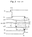
sense amplifier 8 of Fig. 2 will be explained next with reference to Fig. 3, where a power supply voltage VCC applied to thesense amplifier 8 is high, for example, 2.5 to 5.5V. - First, at time t1, the-sense activation signal S is changed from low to high. As a result, the internal sense activation signal generating circuit 838 is set, so that the internal sense activation signal SI rises at time t2. Thus, the
amplifier circuits - In the
amplifier circuit 81, since thecurrent mirror circuits D is gradually decreased. On the other hand, in theamplifier circuit 82, the potential at the data lines DOI andDOI are both gradually decreased, but the potential at one of the bit lines such asDOI is again increased. - In the
sense detection circuit 83, when at least one of the potentials at the data line DOI andDOI becomes lower than the operating point Vth, theNAND circuits DOI becomes lower than the operating point Vth, so that the sense detection signal N of theinverter 831 rises. Therefore, at time t4, when a time d corresponding to the delay time of thedelay circuit 841 has passed, the sense end signal SE rises to reset the internal sense activationsignal generating circuit 85, and accordingly, the internal sense activation signal SI falls to deactivate theamplifiers - In Fig. 3, the output data DO is already established at time t5 early enough before time t4, which causes no problem.
- The operation of the
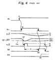
sense amplifier 8 of Fig. 2 will be explained next with reference to Fig. 4, where the power supply voltage VCC applied to thesense amplifier 8 is low, for example, 1.5V. - First, at time t1, the sense activation signal S is changed from low to high. As a result, the internal sense activation
signal generating circuit 85 is set, so that the internal sense activation signal SI rises at time t2. Thus, theamplifier circuits - In the
amplifier circuit 81, although the potential at one of the data lines such as D remains at a high level, the potential at the other data line such asD is gradually decreased. On the other hand, in theamplifier circuit 82, the potentials at the data lines DOI andDOI are both gradually decreased, but the potential at one of the bit lines such asDOI is again increased. - In this case, since the power supply voltage VCC is very low, at time t3' earlier than time t3 of Fig. 3 the potentials at the data lines DOI and
DOI both become lower than the operating point Vth, so that the sense detection signal N of theinverter 831 and the potential at the outputN of theinverter 832 both rise. Therefore, at time t4' earlier than time t4 of Fig. 3, when a time d corresponding to the delay time of thedelay circuit signal generating circuit 85, and accordingly, the internal sense activation signal SI falls to deactivate theamplifiers - In Fig. 4, however, the output data DO will be established at time t5 late enough after time t4'. Therefore, a normal output data DO cannot be obtained.
- If Fig. 5, which illustrates a first embodiment of the present invention, a masking
circuit 86 is interposed between thesense detection circuit 83 and the sense and signal generatingcircuit 84 of Fig. 2. That is, when theinverters N , the maskingcircuit 86 disables the sense detection signal N and N, so that the sense endsignal generating circuit 84 is not operated. - The masking
circuit 86 is formed by a NORcircuit 861 connected to the data lines DOI andDOI for generating a mask signal MSK. Note that the NORcircuit 861 has the same operating point Vth as that of theinverters DOI are both lower than the operating point Vth, is the mask signal MSK made high. Also, the maskingcircuit 86 is formed by twoinverters inverters circuit 864 connected to the NORcircuit 861 and theinverter 862, and a NORcircuit 865 connected to the NORcircuit 861 and theinverter 863. In this case, when the mask signal MSK is high, the outputs of the NORcircuits N . Contrary to this, when the mask signal MSK is low, the outputs of the NORcircuits inverters sense amplifier 8 of Fig. 5 operates in the same way as that of Fig. 2. Therefore, when the power supply voltage applied to thesense amplifier 8 of Fig. 5 is high, since the potentials at the data lines DOI andDOI are not lower than the operating point Vth simultaneously, the maskingcircuit 86 is not operated, which also causes no problem. - The operation of the
sense amplifier 8 of Fig. 5 will be explained next with reference to Fig. 6, where the power supply voltage VCC applied to thesense amplifier 8 is low, for example, 1.5V. - First, at time t1, the sense activation signal S is changed from low to high. As a result, the internal sense activation
signal generating circuit 85 is set, so that the internal sense activation signal SI rises at time t2. Thus, theamplifier circuits - In the
amplifier circuit 81, although the potential at one of the data lines such as D remains at a high level, the potential at the other data line such asD is gradually decreased. On the other hand, in theamplifier circuit 82, the potentials at the data lines DOI andDOI are both gradually decreased, but the potential at one of the bit lines such asDOI is again increased. - In this case, since the power supply voltage VCC is very low, at time t3, the potentials at the data lines DOI and
DOI both becomes lower than the operating point Vth, so that the sense detection signals N andN both rise, and accordingly, the potentials A andA at the outputs of theinverters N1 of the NORcircuits A . - Next, at time t4, when the potential at the data line DOI becomes higher than the operating point Vth while the potential at the data line
DOI remains lower than the operating point Vth, the mask signal MSK is made low. In this case, the sense detection signals N andN and the outputs A andA of theinverters - Therefore, at time t5, when a time d corresponding to the delay time of the
delay circuits signal generating circuit 85, and accordingly, the internal sense activation signal SI falls to deactivate theamplifiers - Even in Fig. 6, the output data DO is already established at time t6 early enough before time t5, which also causes no problem.
- Note that the avove-mentioned delay time of the
delay circuits - Thus, in the first embodiment, when the power suply voltage VCC is low, even if detection signals N and
N are both generated, a mask signal MSK is generated to delay the generation of a sense end signal SE. Thus, the timing of generation of the output data DO can be sufficiently before that of the sense end signal SE, thus making the output data DO normal. - In Fig. 7, which illustrates a second embodiment of the present invention, the masking
circuit 86 of Fig. 5 is modified into a masking circuit 86'. The masking circuit 86' is formed by a NAND circuit 861', a NAND circuit 862' and an inverter 863' serving as an AND circuit, a NAND circuit 864' and an inverter 865' serving as an AND circuit, and delay circuits 866' and 867'. NOte that the delay circuits 866' and 867' have a delay time which is approximately the same as the operation time of the NAND circuit 861'. Even in Fig. 7, when the sense detection signals N and N are both high, the NAND circuit 861' generates a mask signal MSK, so that the outputs N1 andN1 of the inverters 863' and 865' are made low regardless of the sense detection signals N andN . Thus, thesense amplifier 8 of Fig. 7 operates in the same way as thesense amplifier 8 of Fig. 5. - Note that the present invention can be applied to a sense amplifier including a single differential amplifier as illustrated in Fig. 8, where the
amplifier 82 is connected directly to the data lines DO andDO . - As explained hereinabove, according to the present invention, even when the power supply voltage is changed, the timing of an output data can be sufficiently before the cut off timing of the sense amplifier. Thus, normal output data can be obtained.
Claims (7)
- A sense amplifier for sensing a difference in potential between first and second data lines (D, D), comprising:an amplifier circuit (81, 82) for amplifying said difference in potential, said amplifier circuit generating first and second output voltages (DOI,
DOI );an amplifier circuit activating circuit (85), connected to said amplifier circuit, for receiving a sense start signal (S) to activate said amplifier circuit and receiving a sense end signal (SE) to deactivate said amplifier circuit;a first sense detecting circuit (831), connected to said amplifier circuit, for determining whether or not said amplifier circuit is activated in accordance with said first output voltage and generating a first sense detection signal (N);a second sense detecting circuit (832), connected to said amplifier circuit, for determining whether or not said amplifier circuit is activated in accordance with said second output voltage and generating a second sense detection signal (N ); anda sense end signal generating circuit (84), connected to said amplifier circuit activating circuit, for receiving at least one of said first and second sense detection signals and generating said sense end signal when a predetermined time (d) has passed after said at least one of said first and second sense detection signals is received; characterised bya masking circuit (86, 86'), connected between said first and second sense detecting circuits and said sense end signal generating circuit, for prohibiting transmission of said first and second sense detection signals to said sense end signal generating circuit only when said first and second sense detection signals are both generated. - The sense amplifier as set forth in claim 1, wherein said masking circuit comprises:a NAND circuit (861'), connected to said first and second sense detecting circuits, for generating a mask signal (MSK);first and second delay circuits (866', 867') connected to said first and second sense detection circuits, respectively and having a delay time which is about the same as an operation time of said first NAND circuit;a first AND circuit (862', 863'), connected to said NAND circuit and said first delay circuit, for transmitting said first sense detection signal to said sense end signal generating circuit in accordance with said mask signal; anda second AND circuit (864', 865'), connected to said NAND circuit and said second delay circuit, for transmitting said second sense detection signal to said sense end signal generating circuit in accordance with said mask signal.
- The sense amplifier as set forth in claim 1, wherein said masking circuit (86) is further connected to said amplifier circuit.
- The sense amplifier as set forth in claim 3, wherein said masking circuit comprises:a first NOR circuit (861), connected to said amplifier circuit, for receiving said first and second output voltages and generating a mask signal (MSK);a first inverter (862) connected to said first sense detecting circuit;a second inverter (862) connected to said second sense detecting circuit;a second NOR circuit (864), connected to said first NOR circuit and said first inverter, for transmitting said first sense detection signal to said sense end signal generating circuit in accordance with said mask signal; anda third NOR circuit (865), connected to said first NOR circuit and said second inverter, for transmitting said second sense detection signal to said sense end signal generating circuit in accordance with said mask signal.
- The sense amplifier as set forth in claim 1, wherein said amplifier circuit comprises:a first stage differential amplifier (81) for amplifying said difference in potential and generating said first and second output voltages; anda second stage differential amplifier (82), connected to said first differential amplifier, for generating a difference between said first and second output voltages.
- The sense amplifier as set forth in claim 1, wherein said amplifier circuit comprises:a single stage differential amplifier (82) for amplifying said difference in potential and generate said first and second output voltages.
- The sense amplifier as set forth in claim 1, wherein each of said first and second sense detecting circuits comprises an inverter.
Applications Claiming Priority (3)
| Application Number | Priority Date | Filing Date | Title |
|---|---|---|---|
| JP22700496 | 1996-08-28 | ||
| JP8227004A JP2845264B2 (en) | 1996-08-28 | 1996-08-28 | Self-cutoff type sense amplifier circuit |
| JP227004/96 | 1996-08-28 |
Publications (2)
| Publication Number | Publication Date |
|---|---|
| EP0827151A1 EP0827151A1 (en) | 1998-03-04 |
| EP0827151B1 true EP0827151B1 (en) | 2002-11-27 |
Family
ID=16854009
Family Applications (1)
| Application Number | Title | Priority Date | Filing Date |
|---|---|---|---|
| EP97114945A Expired - Lifetime EP0827151B1 (en) | 1996-08-28 | 1997-08-28 | Self cut-off type sense amplifier operable over a wide range of power supply voltages |
Country Status (5)
| Country | Link |
|---|---|
| US (1) | US5872465A (en) |
| EP (1) | EP0827151B1 (en) |
| JP (1) | JP2845264B2 (en) |
| KR (1) | KR100263256B1 (en) |
| DE (1) | DE69717370D1 (en) |
Families Citing this family (11)
| Publication number | Priority date | Publication date | Assignee | Title |
|---|---|---|---|---|
| US6025741A (en) * | 1996-12-23 | 2000-02-15 | International Business Machines Corporation | Conditional restore for execution unit |
| KR100275132B1 (en) * | 1997-06-24 | 2000-12-15 | 김영환 | Current-mirror type sense amplifier |
| US6282137B1 (en) * | 1999-09-14 | 2001-08-28 | Agere Systems Guardian Corp. | SRAM method and apparatus |
| JP2001101872A (en) | 1999-09-30 | 2001-04-13 | Mitsubishi Electric Corp | Amplifier circuit |
| US6304107B1 (en) * | 2000-02-25 | 2001-10-16 | Lsi Logic Corporation | Comparator metastability performance from an enhanced comparator detection circuit |
| DE10219649C1 (en) * | 2002-05-02 | 2003-11-27 | Infineon Technologies Ag | Differential current evaluation circuit and sense amplifier circuit for evaluating a memory state of an SRAM semiconductor memory cell |
| KR100483028B1 (en) * | 2003-03-19 | 2005-04-15 | 주식회사 하이닉스반도체 | Ferroelectric memory cell and memory device using the same |
| EP2124337B1 (en) * | 2008-05-23 | 2016-04-27 | Zoran Corporation | Latched comparator circuit |
| US8319526B2 (en) | 2009-11-17 | 2012-11-27 | Csr Technology Inc. | Latched comparator circuit |
| KR20130123934A (en) * | 2012-05-04 | 2013-11-13 | 에스케이하이닉스 주식회사 | Input output sense amplifier and semiconductor apparatus including the same |
| CN116430102B (en) * | 2023-06-14 | 2023-08-29 | 苏州贝克微电子股份有限公司 | Voltage detection circuit with wide input voltage range |
Family Cites Families (7)
| Publication number | Priority date | Publication date | Assignee | Title |
|---|---|---|---|---|
| IT1238022B (en) * | 1989-12-22 | 1993-06-23 | Cselt Centro Studi Lab Telecom | DIFFERENTIAL VOLTAGE DISCRIMINATOR IN C-MOS TECHNOLOGY. |
| US4972374A (en) * | 1989-12-27 | 1990-11-20 | Motorola, Inc. | Output amplifying stage with power saving feature |
| JPH04278288A (en) * | 1991-03-07 | 1992-10-02 | Toshiba Corp | Semiconductor memory |
| JPH05325569A (en) * | 1992-05-27 | 1993-12-10 | Toshiba Corp | Semiconductor storage device |
| JP3307009B2 (en) * | 1993-07-21 | 2002-07-24 | 富士通株式会社 | Semiconductor storage device |
| US5737273A (en) * | 1995-04-06 | 1998-04-07 | Ricoh Company, Ltd. | Sense amplifier and reading circuit with sense amplifier |
| US5615158A (en) * | 1995-11-13 | 1997-03-25 | Micron Technology, Inc. | Sense amplifier circuit for detecting degradation of digit lines and method thereof |
-
1996
- 1996-08-28 JP JP8227004A patent/JP2845264B2/en not_active Expired - Fee Related
-
1997
- 1997-08-27 US US08/917,883 patent/US5872465A/en not_active Expired - Fee Related
- 1997-08-28 KR KR1019970045784A patent/KR100263256B1/en not_active IP Right Cessation
- 1997-08-28 DE DE69717370T patent/DE69717370D1/en not_active Expired - Lifetime
- 1997-08-28 EP EP97114945A patent/EP0827151B1/en not_active Expired - Lifetime
Also Published As
| Publication number | Publication date |
|---|---|
| JP2845264B2 (en) | 1999-01-13 |
| KR100263256B1 (en) | 2000-08-01 |
| US5872465A (en) | 1999-02-16 |
| KR19980019216A (en) | 1998-06-05 |
| DE69717370D1 (en) | 2003-01-09 |
| JPH1069785A (en) | 1998-03-10 |
| EP0827151A1 (en) | 1998-03-04 |
Similar Documents
| Publication | Publication Date | Title |
|---|---|---|
| US7855926B2 (en) | Semiconductor memory device having local sense amplifier with on/off control | |
| JP4339532B2 (en) | Static memory with self-timing circuit | |
| US5455803A (en) | Semiconductor device which operates at a frequency controlled by an external clock signal | |
| US20060221726A1 (en) | Over driving control signal generator in semiconductor memory device | |
| US5014245A (en) | Dynamic random access memory and method for writing data thereto | |
| JPH05325540A (en) | Semiconductor storage circuit | |
| EP0827151B1 (en) | Self cut-off type sense amplifier operable over a wide range of power supply voltages | |
| KR100297717B1 (en) | I/O sense amplifier of semiconductor memory and semiconductor memory using the same | |
| WO1996015535A1 (en) | Bitline level insensitive sense amplifier | |
| US5576641A (en) | Output buffer | |
| US6411559B1 (en) | Semiconductor memory device including a sense amplifier | |
| US5883851A (en) | Semiconductor memory device and a reading method thereof | |
| JP2718577B2 (en) | Dynamic RAM | |
| KR100402388B1 (en) | Semiconductor memory device having reduced chip select output time | |
| US6366492B1 (en) | Semiconductor memory device capable of automatically controlling bit-line recovery operation | |
| US5648932A (en) | Output control circuit for semiconductor memory | |
| US6169702B1 (en) | Memory device having a chip select speedup feature and associated methods | |
| JP3169819B2 (en) | Semiconductor storage device | |
| US5355349A (en) | Semiconductor integrated circuit device | |
| US5973987A (en) | Semiconductor memory device delaying ATD pulse signal to generate word line activation signal | |
| KR100301820B1 (en) | Sense amplifier | |
| JP3192709B2 (en) | Semiconductor storage device | |
| US6304491B2 (en) | Integrated semiconductor memory | |
| KR100431304B1 (en) | A static random access memory with improved read performance | |
| KR100483058B1 (en) | Lath buffer device for semiconductor memory device |
Legal Events
| Date | Code | Title | Description |
|---|---|---|---|
| PUAI | Public reference made under article 153(3) epc to a published international application that has entered the european phase |
Free format text: ORIGINAL CODE: 0009012 |
|
| AK | Designated contracting states |
Kind code of ref document: A1 Designated state(s): DE FR GB |
|
| 17P | Request for examination filed |
Effective date: 19980520 |
|
| AKX | Designation fees paid |
Free format text: DE FR GB |
|
| RBV | Designated contracting states (corrected) |
Designated state(s): DE FR GB |
|
| GRAG | Despatch of communication of intention to grant |
Free format text: ORIGINAL CODE: EPIDOS AGRA |
|
| 17Q | First examination report despatched |
Effective date: 20011129 |
|
| GRAG | Despatch of communication of intention to grant |
Free format text: ORIGINAL CODE: EPIDOS AGRA |
|
| GRAG | Despatch of communication of intention to grant |
Free format text: ORIGINAL CODE: EPIDOS AGRA |
|
| GRAH | Despatch of communication of intention to grant a patent |
Free format text: ORIGINAL CODE: EPIDOS IGRA |
|
| GRAH | Despatch of communication of intention to grant a patent |
Free format text: ORIGINAL CODE: EPIDOS IGRA |
|
| GRAA | (expected) grant |
Free format text: ORIGINAL CODE: 0009210 |
|
| AK | Designated contracting states |
Kind code of ref document: B1 Designated state(s): DE FR GB |
|
| PG25 | Lapsed in a contracting state [announced via postgrant information from national office to epo] |
Ref country code: FR Free format text: LAPSE BECAUSE OF FAILURE TO SUBMIT A TRANSLATION OF THE DESCRIPTION OR TO PAY THE FEE WITHIN THE PRESCRIBED TIME-LIMIT Effective date: 20021127 |
|
| REG | Reference to a national code |
Ref country code: GB Ref legal event code: FG4D |
|
| REF | Corresponds to: |
Ref document number: 69717370 Country of ref document: DE Date of ref document: 20030109 |
|
| PG25 | Lapsed in a contracting state [announced via postgrant information from national office to epo] |
Ref country code: DE Free format text: LAPSE BECAUSE OF FAILURE TO SUBMIT A TRANSLATION OF THE DESCRIPTION OR TO PAY THE FEE WITHIN THE PRESCRIBED TIME-LIMIT Effective date: 20030228 |
|
| PG25 | Lapsed in a contracting state [announced via postgrant information from national office to epo] |
Ref country code: GB Free format text: LAPSE BECAUSE OF NON-PAYMENT OF DUE FEES Effective date: 20030828 |
|
| EN | Fr: translation not filed | ||
| PLBE | No opposition filed within time limit |
Free format text: ORIGINAL CODE: 0009261 |
|
| STAA | Information on the status of an ep patent application or granted ep patent |
Free format text: STATUS: NO OPPOSITION FILED WITHIN TIME LIMIT |
|
| 26N | No opposition filed |
Effective date: 20030828 |
|
| GBPC | Gb: european patent ceased through non-payment of renewal fee |