EP0824705B1 - Strahlungssensor zur bestimmung der einfallsrichtung - Google Patents
Strahlungssensor zur bestimmung der einfallsrichtung Download PDFInfo
- Publication number
- EP0824705B1 EP0824705B1 EP96915284A EP96915284A EP0824705B1 EP 0824705 B1 EP0824705 B1 EP 0824705B1 EP 96915284 A EP96915284 A EP 96915284A EP 96915284 A EP96915284 A EP 96915284A EP 0824705 B1 EP0824705 B1 EP 0824705B1
- Authority
- EP
- European Patent Office
- Prior art keywords
- radiation sensor
- radiation
- incidence
- sensor
- photodiode
- Prior art date
- Legal status (The legal status is an assumption and is not a legal conclusion. Google has not performed a legal analysis and makes no representation as to the accuracy of the status listed.)
- Expired - Lifetime
Links
Images


Classifications
-
- G—PHYSICS
- G01—MEASURING; TESTING
- G01S—RADIO DIRECTION-FINDING; RADIO NAVIGATION; DETERMINING DISTANCE OR VELOCITY BY USE OF RADIO WAVES; LOCATING OR PRESENCE-DETECTING BY USE OF THE REFLECTION OR RERADIATION OF RADIO WAVES; ANALOGOUS ARRANGEMENTS USING OTHER WAVES
- G01S3/00—Direction-finders for determining the direction from which infrasonic, sonic, ultrasonic or electromagnetic waves, or particle emission, not having a directional significance, are being received
- G01S3/78—Direction-finders for determining the direction from which infrasonic, sonic, ultrasonic or electromagnetic waves, or particle emission, not having a directional significance, are being received using electromagnetic waves other than radio waves
- G01S3/782—Systems for determining direction or deviation from predetermined direction
- G01S3/783—Systems for determining direction or deviation from predetermined direction using amplitude comparison of signals derived from static detectors or detector systems
-
- G—PHYSICS
- G01—MEASURING; TESTING
- G01S—RADIO DIRECTION-FINDING; RADIO NAVIGATION; DETERMINING DISTANCE OR VELOCITY BY USE OF RADIO WAVES; LOCATING OR PRESENCE-DETECTING BY USE OF THE REFLECTION OR RERADIATION OF RADIO WAVES; ANALOGOUS ARRANGEMENTS USING OTHER WAVES
- G01S3/00—Direction-finders for determining the direction from which infrasonic, sonic, ultrasonic or electromagnetic waves, or particle emission, not having a directional significance, are being received
- G01S3/78—Direction-finders for determining the direction from which infrasonic, sonic, ultrasonic or electromagnetic waves, or particle emission, not having a directional significance, are being received using electromagnetic waves other than radio waves
- G01S3/781—Details
-
- G—PHYSICS
- G01—MEASURING; TESTING
- G01S—RADIO DIRECTION-FINDING; RADIO NAVIGATION; DETERMINING DISTANCE OR VELOCITY BY USE OF RADIO WAVES; LOCATING OR PRESENCE-DETECTING BY USE OF THE REFLECTION OR RERADIATION OF RADIO WAVES; ANALOGOUS ARRANGEMENTS USING OTHER WAVES
- G01S3/00—Direction-finders for determining the direction from which infrasonic, sonic, ultrasonic or electromagnetic waves, or particle emission, not having a directional significance, are being received
- G01S3/78—Direction-finders for determining the direction from which infrasonic, sonic, ultrasonic or electromagnetic waves, or particle emission, not having a directional significance, are being received using electromagnetic waves other than radio waves
- G01S3/782—Systems for determining direction or deviation from predetermined direction
- G01S3/783—Systems for determining direction or deviation from predetermined direction using amplitude comparison of signals derived from static detectors or detector systems
- G01S3/784—Systems for determining direction or deviation from predetermined direction using amplitude comparison of signals derived from static detectors or detector systems using a mosaic of detectors
Definitions
- the present invention relates to a radiation sensor for determining the direction of incident radiation.
- the starting point has especially been to provide a radiation sensor of the type concerned that can be used in military laser warning contexts.
- the radiation sensor can of course also be used in other contexts.
- the range within which one could want the wamer to function is within the irradiance extremes 10 mW/m 2 and 10 GW/m 2 , i.e. the dynamic range amounts to 120 dB. If a range from 10 W/m 2 to 1 GW/m 2 is sufficient, the dynamic range will be 80 dB, which may be said to be a more reasonable value, but still a range that is technically difficult to measure.
- the illumination is in most cases pulsed and the pulses are very short (nanoseconds).
- PSD position sensing detector
- PSD detectors are not intended for so short pulses as those involved in laser warning contexts and, besides, their dynamic range is restricted, which means that commercially available detectors of this type cannot be used for the intended purpose.
- a measuring device having photodiodes along a line in a plane within which the angle of incidence is intended to be measured.
- a slit causes incident radiation to illuminate different parts of the line of photodiodes in dependence on the direction of incidence of the radiation.
- the measuring device does not have the desired properties defined in the beginning of the description.
- the basic idea in the invention is to create, by discrete elements, a PSD-like sensor construction, see Fig. 1, in which photodiodes are designated D and resistors R and R a .
- a number of photodiodes D are connected between the junction points between a number of equally large resistors R in a chain of resistors and a bias source, which is selected such that the photodiodes are reverse-biased.
- the photodiodes are physically distributed at equal distances along a line in a plane within which the angle of incidence is intended to be measured.
- incident radiation can be made to illuminate different parts of this row of detectors 2 in dependence on the direction of incidence of the radiation.
- signals can be taken out, whose relationship can be made to constitute a measure of where along the detector row of photodiodes the main focus of the radiation is located. It is possible to measure the currents at the ends of the chain of resistors.
- the voltage across the two resistors R a at the tapping points A1 and A2 are measured by means of a fix reference potential V1 and the resistors R a . The ratio between these voltages determines the position of the point of illumination.
- the senor suffers from a number of shortcomings.
- the capacitance of the photodiodes D combined with the resistors R will function as a lowpass RC filter. This implies in turn that the stated bearing towards the source of illumination will depend on the pulse length of the source and, in an incorrect manner, by the position of the illumination along the line of photodiodes. This is disadvantageous.
- the bias of the photodiodes decreases with the distance from the tapping points A1, A2, which is not desirable, since the bias should be as great as possible, thereby obtaining a quick response of the photodiodes to the incident radiation.
- the signal must be conducted merely from an active photodiode D via the chain of resistors out to the tapping points, without being conducted into non-active photodiodes. It is therefore necessary to introduce some sort of blocking device for the propagation of signals in undesired directions.
- Fig. 2 indicates a solution to the problem.
- the solution is presented, implemented by means of NPN transistors, but it may, of course, also be implemented by means of PNP transistors. Necessary changes in the circuit diagram, such as the arrangement of components and bias, are obvious to those skilled in the art.
- each photodiode is supplemented with a current-limiting resistor R sb , a bias resistor R fs , and a transistor T.
- the transistor which is chosen to have as low capacitance as possible, operates according to the technique "common base", the base being on earth potential.
- the photodiode is arranged on the emitter of the transistor.
- the transistors T prevent, owing to low capacitance, parts of the signal current from leaking out, on its way through the chain of resistors, through connections of non-illuminated photodiodes.
- the bias resistor R fs gives the transistor bias for a suitable working range.
- the maximum current through the transistor and thus out to the chain of resistors R is limited.
- the position-determining currents are measured at the resistors R a and can be given a suitable size so as not to accomplish saturation in any succeeding amplifiers even at a maximum level of illumination.
- the currents can be very long relative to the length of the light pulse, since basically the charge excited in the photodiode is proportional to the light energy that may vary by several ten decibels.
- this design can only determine the direction of incidence in one plane, for instance, in the lateral direction, and for determining the vertical direction, it is necessary to add an identical device, whose optical properties are directed perpendicular to those of the first-mentioned.
- a warning device can calculate the intensity of incoming illumination. It is then possible to estimate whether the laser illumination concerns the platform carrying the warning device, or some other target.
- the inventive sensor construction has eliminated the possibility of measuring, in the entire dynamic range, an amplitude which in this respect is correct. In the range of saturated photodiodes, the intensity of illumination is instead reflected in an increased pulse length by the excited charge being let out gradually. However, this pulse length is easy to measure and calibrate, and therefore the invention also complies with this wish.
- FIG. 2 A sensor according to Fig. 2 has been illuminated and tested.
- the signal quotient calculated from the measured peak values is illustrated in Fig. 3, where a straight line, representing the ideal outcome, is also drawn.
- Fig. 4 A further processing of the values to show the angular error relative to the theoretically correct value is shown in Fig. 4.
- Fig. 4 use has been made of peak value measurement for calculating the result.
- a last step according to the invention is to make the laser light fall on the detector row 2 in a position dependent on the direction of incidence.
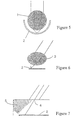
- Fig. 5 illustrates an arrangement having a cylindrical lens 1 and a curved detector row of the above discussed type.
- Fig. 6 shows instead a one-dimensional fish-eye lens 3 together with a planar detector row according to the invention. These two alternatives give a certain optical amplification and are in many cases possible to use.
- a drawback of at least the alternative in Fig. 5 is, however, that central rays and marginal rays do not have the same focus, which especially in the case of high light intensities can result in a false response when calculating the angle of incidence.
- Fig. 7 shows a simple arrangement having a slit 4 in front of a detector row 2 according to the invention. In this case, it may be convenient to provide the detector casing with internal baffles 5 for suppressing reflections in the detector casing.
- the light-sensitive detector row 2 can be replaced by a fibre bundle which conducts the light to a detector row provided with electronics and placed in a shielding.
- the wavelength range within which the construction functions is in known manner restricted by the selected type of detector material.
- the range can readily be extended by parallel mounting of a plurality of detector rows made of materials that are sensitive to different wavelengths.
- a construction having a slit as shown in Fig. 7 is best suited since no wavelength-dependent optical complications will then occur.
- a sensor according to the invention can, within a great dynamic range - about 80 dB - in respect of light intensity, with great accuracy - ⁇ 1° - and via only one signal path, determine the direction of incidence in one dimension for incident light - pulsed or continuous - for wavelengths and pulse lengths within the sensitivity range of the photodiodes.
Landscapes
- Physics & Mathematics (AREA)
- Electromagnetism (AREA)
- Engineering & Computer Science (AREA)
- General Physics & Mathematics (AREA)
- Radar, Positioning & Navigation (AREA)
- Remote Sensing (AREA)
- Light Receiving Elements (AREA)
- Photometry And Measurement Of Optical Pulse Characteristics (AREA)
- Solid State Image Pick-Up Elements (AREA)
- Length Measuring Devices By Optical Means (AREA)
- Investigating Or Analysing Materials By Optical Means (AREA)
Claims (10)
- Strahlungssensor, der die Richtung des Einfalls der Strahlung bestimmt und der eine Anzahl von Photodetektoren, die äquidistant voneinander entlang einer Linie (2) in einer Ebene beabstandet sind, in der der Einfallswinkel gemessen werden soll, und ein optisches Element (1, 3, 4) aufweist, das verursacht, dass die einfallende Strahlung unterschiedliche Teile der Linie aus Photodetektoren in Abhängigkeit von der Richtung des Strahlungseinfalls beleuchtet, dadurch gekennzeichnet, dass er eine Anzahl von gleich großen Widerständen (R) in einer Kette aus Widerständen zwischen zwei Abzweigpunkten (A1, A2) für Sensorsignale aufweist und dass jeder Photodetektor eine Photodiode (D) aufweist, wobei die Photodioden zwischen den Übergangspunkten zwischen den Widerständen in der Widerstandskette und einer gemeinsamen Vorspannungsquelle (Bias) verbunden sind, wobei eine Photodiode mit jedem Übergangspunkt verbunden ist und wobei die Vorspannungsquelle eine Sperrspannung für die Photodioden erzeugt.
- Strahlungssensor, wie im Anspruch 1 beansprucht, dadurch gekennzeichnet, dass ein Transistor (T) niedriger Kapazität in Serie mit jeder Photodiode (D) angeordnet ist und als Blockiereinrichtung arbeitet, die verhindert, dass ein Signalstrom aus der Widerstandskette abgezweigt wird.
- Strahlungssensor, wie im Anspruch 2 beansprucht, dadurch gekennzeichnet, dass der strombegrenzende Widerstand (Rsb) in Serie mit jeder Photodiode (D) und dem Transistor (T) angeordnet ist und den Signalstrom an Verstärker anpasst, die der Widerstandskette nachfolgen.
- Strahlungssensor, wie in einem der vorhergehenden Ansprüche beansprucht, dadurch gekennzeichnet, dass er für die Bestimmung der Signalintensität der einfallenden Strahlung auf der Basis der gemessenen Impulslänge in dem Bereich der gesättigten Photodioden ausgelegt ist.
- Strahlungssensor, wie in einem der vorhergehenden Ansprüche beansprucht, dadurch gekennzeichnet, dass er einen zusätzlichen Sensor aufweist, dessen Längsachse im wesentlichen rechtwinklig zu der Längsachse des ersten Sensors ist.
- Strahlungssensor, wie in einem der Ansprüche 1-5 beansprucht, dadurch gekennzeichnet, dass das optische Element eine zylindrische Linse (1) ist.
- Strahlungssensor, wie im Anspruch 6 beansprucht, dadurch gekennzeichnet, dass die Photodetektoren (D) entlang eines kreisförmigen Bogens verteilt sind, der konzentrisch zu der Linse (1) ist.
- Strahlungssensor, wie in einem der Ansprüche 1-5 beansprucht, dadurch gekennzeichnet, dass das optische Element eine eindimensionale Fischaugenlinse (3) ist.
- Strahlungssensor, wie in einem der Ansprüche 1-5 beansprucht, dadurch gekennzeichnet, dass das optische Element eine Fläche mit einem Schlitz (4) ist, der rechtwinklig zu der Ebene liegt, in der die Richtung des Einfalls gemessen werden soll.
- Strahlungssensor, wie in einem der vorhergehenden Ansprüche beansprucht, dadurch gekennzeichnet, dass der Photodetektor eine optische Faser aufweist, die ein Detektionsende in der Position des Photodetektors in der Linie (2), in der der Einfallswinkel gemessen werden soll, und ein weiteres Ende an einer anderen Stelle hat, das mit der Photodiode (D) verbunden ist.
Applications Claiming Priority (3)
| Application Number | Priority Date | Filing Date | Title |
|---|---|---|---|
| SE9501700 | 1995-05-08 | ||
| SE9501700A SE504365C2 (sv) | 1995-05-08 | 1995-05-08 | Infallsriktningsbestämmande strålningssensor |
| PCT/SE1996/000599 WO1996035959A1 (en) | 1995-05-08 | 1996-05-08 | Radiation sensor determining the direction of incidence |
Publications (2)
| Publication Number | Publication Date |
|---|---|
| EP0824705A1 EP0824705A1 (de) | 1998-02-25 |
| EP0824705B1 true EP0824705B1 (de) | 2002-02-06 |
Family
ID=20398234
Family Applications (1)
| Application Number | Title | Priority Date | Filing Date |
|---|---|---|---|
| EP96915284A Expired - Lifetime EP0824705B1 (de) | 1995-05-08 | 1996-05-08 | Strahlungssensor zur bestimmung der einfallsrichtung |
Country Status (6)
| Country | Link |
|---|---|
| US (1) | US6054715A (de) |
| EP (1) | EP0824705B1 (de) |
| AU (1) | AU5709396A (de) |
| DE (1) | DE69619107T2 (de) |
| SE (1) | SE504365C2 (de) |
| WO (1) | WO1996035959A1 (de) |
Families Citing this family (2)
| Publication number | Priority date | Publication date | Assignee | Title |
|---|---|---|---|---|
| ES2126507B1 (es) * | 1997-01-03 | 1999-12-01 | Garcia Ramon Ferreiro | Sensor de direccion basado en efecto fotovoltaico. |
| WO2002058103A2 (en) | 2001-01-17 | 2002-07-25 | Varian Semiconductor Equipment Associates, Inc. | In situ ion beam incidence angle and beam divergence monitor |
Family Cites Families (5)
| Publication number | Priority date | Publication date | Assignee | Title |
|---|---|---|---|---|
| US4136568A (en) * | 1977-07-15 | 1979-01-30 | Grumman Aerospace Corporation | Electro-optic space positioner |
| FR2450463A1 (fr) * | 1979-02-27 | 1980-09-26 | Thomson Csf | Dispositif optoelectrique de localisation de source rayonnante et systemes comportant de tels dispositifs |
| DE3802450A1 (de) * | 1988-01-28 | 1989-08-10 | Standard Elektrik Lorenz Ag | Schaltungsanordnung zum bewerten der ausgangssignale einer fotodiodeneinheit |
| DE3922017A1 (de) * | 1989-07-05 | 1991-01-17 | Messerschmitt Boelkow Blohm | Optische sensoreinrichtung |
| FR2709840B1 (fr) * | 1993-09-10 | 1995-10-20 | Thomson Csf | Dispositif optique de type fish-eye pour la détection et la localisation d'une source rayonnante. |
-
1995
- 1995-05-08 SE SE9501700A patent/SE504365C2/sv not_active IP Right Cessation
-
1996
- 1996-05-08 WO PCT/SE1996/000599 patent/WO1996035959A1/en not_active Ceased
- 1996-05-08 AU AU57093/96A patent/AU5709396A/en not_active Abandoned
- 1996-05-08 DE DE69619107T patent/DE69619107T2/de not_active Expired - Lifetime
- 1996-05-08 EP EP96915284A patent/EP0824705B1/de not_active Expired - Lifetime
- 1996-05-08 US US08/952,120 patent/US6054715A/en not_active Expired - Lifetime
Also Published As
| Publication number | Publication date |
|---|---|
| AU5709396A (en) | 1996-11-29 |
| SE9501700L (sv) | 1996-11-09 |
| WO1996035959A1 (en) | 1996-11-14 |
| EP0824705A1 (de) | 1998-02-25 |
| DE69619107T2 (de) | 2002-10-31 |
| US6054715A (en) | 2000-04-25 |
| DE69619107D1 (de) | 2002-03-21 |
| SE504365C2 (sv) | 1997-01-20 |
Similar Documents
| Publication | Publication Date | Title |
|---|---|---|
| US9411049B2 (en) | Proximity sensor having array of geiger mode avalanche photodiodes for estimating distance of an object to the array based on at least one of a dark current and a rate of current spikes generated in dark conditions | |
| US6438296B1 (en) | Fiber optic taper coupled position sensing module | |
| US11105626B2 (en) | Position-sensitive optoelectronic detector arrangement, and laser beam receiver using same comprising an elongated light guiding structure between an elongated window and light sensitive regions | |
| JP2016170114A (ja) | 距離測定装置及び光検出器 | |
| CN110836724A (zh) | 光学装置 | |
| CS100589A2 (en) | Method of speed measuring and device for this method realization | |
| US6054715A (en) | Radiation sensor determining the direction of incidence | |
| GB2083313A (en) | Distance detecting device | |
| JP2004361411A (ja) | 受光装置 | |
| JP3215232B2 (ja) | 光電式距離センサ | |
| JP4546047B2 (ja) | 光学距離測定デバイス | |
| JP3270176B2 (ja) | 三角測距式光電センサ | |
| EP0610198B1 (de) | Opto-elektronische messskala | |
| GB2288015A (en) | An optical encoder with an improved photodiode array | |
| JP3001293B2 (ja) | 測距装置 | |
| JP3117227B2 (ja) | 距離検出装置 | |
| GB1571625A (en) | Wheel alignment apparatus | |
| JPH06249649A (ja) | 三角測距式光電センサ | |
| JP2901748B2 (ja) | 距離測定装置 | |
| JPH06241785A (ja) | 三角測距式光電センサ | |
| JP2901747B2 (ja) | 距離測定装置 | |
| JP2882398B2 (ja) | 人工衛星搭載用地球センサ検出器 | |
| JPH04268816A (ja) | 物体検出用光電スイッチ | |
| JP2020042049A (ja) | 距離測定装置及び光検出器 | |
| JPH07286815A (ja) | 位置検出装置 |
Legal Events
| Date | Code | Title | Description |
|---|---|---|---|
| PUAI | Public reference made under article 153(3) epc to a published international application that has entered the european phase |
Free format text: ORIGINAL CODE: 0009012 |
|
| 17P | Request for examination filed |
Effective date: 19971120 |
|
| AK | Designated contracting states |
Kind code of ref document: A1 Designated state(s): BE DE FR GB NL |
|
| 17Q | First examination report despatched |
Effective date: 20000912 |
|
| GRAG | Despatch of communication of intention to grant |
Free format text: ORIGINAL CODE: EPIDOS AGRA |
|
| GRAG | Despatch of communication of intention to grant |
Free format text: ORIGINAL CODE: EPIDOS AGRA |
|
| GRAH | Despatch of communication of intention to grant a patent |
Free format text: ORIGINAL CODE: EPIDOS IGRA |
|
| RAP1 | Party data changed (applicant data changed or rights of an application transferred) |
Owner name: SIMRAD OPTRONICS ASA |
|
| RIN1 | Information on inventor provided before grant (corrected) |
Inventor name: MANNERSKOG, GUNNAR Inventor name: NISSBORG, KURT |
|
| GRAH | Despatch of communication of intention to grant a patent |
Free format text: ORIGINAL CODE: EPIDOS IGRA |
|
| GRAA | (expected) grant |
Free format text: ORIGINAL CODE: 0009210 |
|
| REG | Reference to a national code |
Ref country code: GB Ref legal event code: IF02 |
|
| AK | Designated contracting states |
Kind code of ref document: B1 Designated state(s): BE DE FR GB NL |
|
| PG25 | Lapsed in a contracting state [announced via postgrant information from national office to epo] |
Ref country code: NL Free format text: LAPSE BECAUSE OF FAILURE TO SUBMIT A TRANSLATION OF THE DESCRIPTION OR TO PAY THE FEE WITHIN THE PRESCRIBED TIME-LIMIT Effective date: 20020206 Ref country code: BE Free format text: LAPSE BECAUSE OF FAILURE TO SUBMIT A TRANSLATION OF THE DESCRIPTION OR TO PAY THE FEE WITHIN THE PRESCRIBED TIME-LIMIT Effective date: 20020206 |
|
| REF | Corresponds to: |
Ref document number: 69619107 Country of ref document: DE Date of ref document: 20020321 |
|
| NLV1 | Nl: lapsed or annulled due to failure to fulfill the requirements of art. 29p and 29m of the patents act | ||
| ET | Fr: translation filed | ||
| PLBE | No opposition filed within time limit |
Free format text: ORIGINAL CODE: 0009261 |
|
| STAA | Information on the status of an ep patent application or granted ep patent |
Free format text: STATUS: NO OPPOSITION FILED WITHIN TIME LIMIT |
|
| 26N | No opposition filed |
Effective date: 20021107 |
|
| PGFP | Annual fee paid to national office [announced via postgrant information from national office to epo] |
Ref country code: GB Payment date: 20140530 Year of fee payment: 19 |
|
| PGFP | Annual fee paid to national office [announced via postgrant information from national office to epo] |
Ref country code: DE Payment date: 20140602 Year of fee payment: 19 |
|
| PGFP | Annual fee paid to national office [announced via postgrant information from national office to epo] |
Ref country code: FR Payment date: 20140528 Year of fee payment: 19 |
|
| REG | Reference to a national code |
Ref country code: DE Ref legal event code: R119 Ref document number: 69619107 Country of ref document: DE |
|
| GBPC | Gb: european patent ceased through non-payment of renewal fee |
Effective date: 20150508 |
|
| REG | Reference to a national code |
Ref country code: FR Ref legal event code: ST Effective date: 20160129 |
|
| PG25 | Lapsed in a contracting state [announced via postgrant information from national office to epo] |
Ref country code: DE Free format text: LAPSE BECAUSE OF NON-PAYMENT OF DUE FEES Effective date: 20151201 Ref country code: GB Free format text: LAPSE BECAUSE OF NON-PAYMENT OF DUE FEES Effective date: 20150508 |
|
| PG25 | Lapsed in a contracting state [announced via postgrant information from national office to epo] |
Ref country code: FR Free format text: LAPSE BECAUSE OF NON-PAYMENT OF DUE FEES Effective date: 20150601 |