EP0817543A2 - Diodeless start circuit of an inverter for gas discharge lamp - Google Patents
Diodeless start circuit of an inverter for gas discharge lamp Download PDFInfo
- Publication number
- EP0817543A2 EP0817543A2 EP97304421A EP97304421A EP0817543A2 EP 0817543 A2 EP0817543 A2 EP 0817543A2 EP 97304421 A EP97304421 A EP 97304421A EP 97304421 A EP97304421 A EP 97304421A EP 0817543 A2 EP0817543 A2 EP 0817543A2
- Authority
- EP
- European Patent Office
- Prior art keywords
- voltage
- circuit
- switch
- coupled
- current
- Prior art date
- Legal status (The legal status is an assumption and is not a legal conclusion. Google has not performed a legal analysis and makes no representation as to the accuracy of the status listed.)
- Withdrawn
Links
- 239000003990 capacitor Substances 0.000 claims abstract description 60
- 238000004804 winding Methods 0.000 claims abstract description 21
- 239000004020 conductor Substances 0.000 claims abstract description 6
- 230000000977 initiatory effect Effects 0.000 claims description 2
- 238000010304 firing Methods 0.000 description 7
- 230000010355 oscillation Effects 0.000 description 5
- 230000002457 bidirectional effect Effects 0.000 description 3
- 230000000630 rising effect Effects 0.000 description 3
- 238000010586 diagram Methods 0.000 description 2
- 238000007599 discharging Methods 0.000 description 2
- 238000006842 Henry reaction Methods 0.000 description 1
- 230000005669 field effect Effects 0.000 description 1
- 230000003993 interaction Effects 0.000 description 1
- 230000003071 parasitic effect Effects 0.000 description 1
- 239000004065 semiconductor Substances 0.000 description 1
Images
Classifications
-
- H—ELECTRICITY
- H05—ELECTRIC TECHNIQUES NOT OTHERWISE PROVIDED FOR
- H05B—ELECTRIC HEATING; ELECTRIC LIGHT SOURCES NOT OTHERWISE PROVIDED FOR; CIRCUIT ARRANGEMENTS FOR ELECTRIC LIGHT SOURCES, IN GENERAL
- H05B41/00—Circuit arrangements or apparatus for igniting or operating discharge lamps
- H05B41/14—Circuit arrangements
- H05B41/26—Circuit arrangements in which the lamp is fed by power derived from dc by means of a converter, e.g. by high-voltage dc
- H05B41/28—Circuit arrangements in which the lamp is fed by power derived from dc by means of a converter, e.g. by high-voltage dc using static converters
- H05B41/282—Circuit arrangements in which the lamp is fed by power derived from dc by means of a converter, e.g. by high-voltage dc using static converters with semiconductor devices
- H05B41/2825—Circuit arrangements in which the lamp is fed by power derived from dc by means of a converter, e.g. by high-voltage dc using static converters with semiconductor devices by means of a bridge converter in the final stage
- H05B41/2827—Circuit arrangements in which the lamp is fed by power derived from dc by means of a converter, e.g. by high-voltage dc using static converters with semiconductor devices by means of a bridge converter in the final stage using specially adapted components in the load circuit, e.g. feed-back transformers, piezoelectric transformers; using specially adapted load circuit configurations
-
- Y—GENERAL TAGGING OF NEW TECHNOLOGICAL DEVELOPMENTS; GENERAL TAGGING OF CROSS-SECTIONAL TECHNOLOGIES SPANNING OVER SEVERAL SECTIONS OF THE IPC; TECHNICAL SUBJECTS COVERED BY FORMER USPC CROSS-REFERENCE ART COLLECTIONS [XRACs] AND DIGESTS
- Y10—TECHNICAL SUBJECTS COVERED BY FORMER USPC
- Y10S—TECHNICAL SUBJECTS COVERED BY FORMER USPC CROSS-REFERENCE ART COLLECTIONS [XRACs] AND DIGESTS
- Y10S315/00—Electric lamp and discharge devices: systems
- Y10S315/05—Starting and operating circuit for fluorescent lamp
Definitions
- the present invention relates to ballast circuits for gas discharge lamps of the type including a d.c. to a.c. converter with a pair of serially connected switches whose operation is controlled by self-resonant feedback circuits. More particularly, the invention relates to a circuit for starting self-resonant operation of a ballast circuit that does not require a p-n diode for preventing during steady state ballast operation the firing of a voltage-breakover switch used to create a starting pulse.
- ballast circuits for gas discharge lamps of the type including a d.c. to a.c. converter with a pair of serially connected switches whose operation is controlled by self-resonant feedback circuits.
- a starting circuit is included to initiate self-resonant oscillation of the ballast circuits. This is accomplished by creating a pulse of current through a voltage-breakover (VB) switch, such as a diac, which is accomplished by biasing the VB switch to its threshold voltage for firing (i.e., becoming conductive).
- VB voltage-breakover
- one typical circuit to accomplish this includes a p-n diode with its cathode connected to the common node between the mentioned pair of switches.
- a p-n diode is included in the starting circuit disclosed in U.S. Patent 4,353,010.
- ballast circuit including a starting circuit that did not require a p-n diode for preventing firing of a VB switch during steady state ballast operation.
- ballast circuits for gas discharge lamps of the type including a d.c. to a.c. converter with a pair of serially connected switches whose operation is controlled by self-resonant feedback circuits, including a starting circuit not requiring a p-n diode to prevent firing of a voltage-breakover switch during steady state ballast operation.
- a further object of the invention is to provide ballast circuits of the foregoing type using readily available circuit components.
- a ballast circuit for a gas discharge lamp comprising a resonant load circuit incorporating a gas discharge lamp and including first and second resonant impedances whose values determine the operating frequency of the resonant load circuit.
- a d.c:to-a.c. converter circuit is coupled to the resonant load circuit so as to induce an a.c. current in the resonant load circuit, and comprises first and second switches serially connected in the mentioned order between a bus conductor at a d.c. bus voltage and ground, and having a common switch node through which the a.c. current flows.
- a bridge capacitor has one end connected to ground.
- First and second feedback circuits regeneratively control the first and second switches, respectively, in response to a.c. current in the resonant load circuit.
- a starting circuit initiates operation of the first and second feedback circuits, and incorporates a voltage-divider network comprising first and second serially connected impedances with a common impedance node, and is coupled between the common switch node and ground.
- Such circuit includes a starting capacitor coupled between the common impedance node and ground, and a voltage-breakover switch coupled between a non-grounded end of the bridge capacitor and the starting capacitor.
- a transformer winding serially coupled to the voltage-breakover switch so as to conduct a pulse of current when the voltage-breakover switch fires, the winding being coupled to the first and second feedback circuits so as to result in a starting pulse of current in the circuits when the voltage-breakover switch fires.
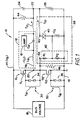
- Fig. 1 is a schematic diagram, partially in block form, of a power supply circuit including feedback circuitry for controlling the conduction states of a pair of switches of a half-bridge converter.
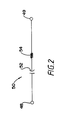
- Fig. 2 is a circuit diagram of a snubber & gate speed-up circuit that may be used in the power supply circuit of Fig. 1.
- Fig. 1 shows a power supply circuit 10 for a resonant load circuit 12.
- Resonant load circuit 12 may include a gas discharge lamp 13, such as a fluorescent lamp.
- Electrical power for resonant load circuit 12 is provided by a bus voltage V B impressed between a d.c. bus conductor 14 and a reference, or ground, conductor 16, which is not necessarily at earth ground.
- Bus voltage V B is provided by a bus voltage generator 18, typically comprising a conventional full-wave rectifier, for rectifying a.c. voltage from an a.c. source, or line, voltage (not shown).
- Bus voltage generator 18, optionally, may include a power factor correction circuit, as is conventional.
- Power supply circuit 10 impresses a bidirectional, resonant load voltage V R across resonant load circuit 12, from left-shown node 20 to right-shown node 22., which, in turn, induces bidirectional current through resonant load circuit 12.
- power supply circuit 10 To generate resonant load voltage V R from d.c. bus voltage V B on d.c. bus 14, power supply circuit 10 conventionally includes a series half-bridge converter, including series-connected MOSFETs (Metal-Oxide-Semiconductor Field-Effect Transistors), or other switches, Q 1 and Q 2 .
- MOSFETs Metal-Oxide-Semiconductor Field-Effect Transistors
- the drain of MOSFET Q 1 is directly connected to d.c. bus 14, and its source is connected to the drain of MOSFET Q 2 at node 20, which is common to switches Q 1 and Q 2 .
- the drain of MOSFET Q 2 is connected to ground 16.
- the conduction states of MOSFETs Q 1 and Q 2 are determined by respective control voltages on the respective gates G 1 and G 2 of the MOSFETs.
- bidirectional, resonant load voltage V R is generated by alternately connecting common node 20 to d.c. bus 14, which is at bus voltage V B , via MOSFET Q 1 , and then to ground 16, via MOSFET Q 2 .
- bridge capacitor 24 may be omitted and replaced with a capacitor (not shown) connected between bus 14 and ground 16, and with bridge capacitor remaining in the position illustrated.
- Control signals are provided on gates G 1 and G 2 of MOSFETs Q 1 and Q 2 by respective feedback circuits 30 and 32.
- Feedback circuits 30 and 32 are responsive to a current from part of resonant load circuit 12 that is sensed by transformer winding T 1C , which is coupled to windings T 1A and T 1B of the feedback circuits. Included in feedback circuits 30 and 32 are respective pairs of back-to-back (i.e. cathode-to-cathode) connected Zener diodes 34 and 36.
- Zener diode pairs clamp the voltage on their respective gates G 1 and G 2 , with respect to the voltage on the lower-shown nodes of their associated switches Q 1 and Q 2 , at a positive or a negative level with a timing determined by the polarity and amplitude of feedback current (not shown) in the respective windings T 1A and T 1B .
- Respective, inherent capacitances (not shown) of the gates G 1 and G 2 also influence the behavior of feedback circuits 30 and 32.
- a starting circuit 38 is provided for initiating oscillation of resonant voltage V R . This is accomplished by providing a pulse of current through a winding T 1D , which is coupled to windings T 1A and T 1B of feedback circuits 30 and 32.
- the pulse of current through winding T 1D occurs when a switch 40 comprising a voltage-breakover (VB) switch, such as a diac, fires (i.e. begins conducting).
- VB voltage-breakover
- the voltage on starting capacitor C S is determined by a voltage-divider network 42, which includes two serially connected impedances, for instance, resistors R 1 and R 2 , connected between node 20 and ground 16, and whose common node is connected to the non-grounded end of starting capacitor C S .
- the first criterion can be expressed by the equation: (R 1 *R 2 /(R 1 + R 2 ))*C S ⁇ 100 times steady state switching frequency, where "*" indicates multiplication, and " ⁇ " means approximately.
- the second criterion is to minimize the power dissipation in resistor R 1 .
- the value for resistor R 2 may be chosen to assure that sufficient voltage exists on capacitor C S to prevent VB switch 40 from firing when bus voltage V B is at a maximum value, and the voltage across VB switch 40 is at a minimum value.
- starting circuit 38 Details of operation of starting circuit 38 are now considered during an initial bus energization phase, a start phase, a steady state phase, and an oscillation-interrupted phase.
- Bridge capacitor 26 charges to about 1 ⁇ 2 of bus voltage V B At typical lamp operating frequencies (e.g., from several kilohertz to 150 kilohertz), with resistors R 1 and R 2 chosen as described above, the voltage on bridge capacitor 26 rises faster than the voltage on starting capacitor C S .
- starting capacitor C S should quickly discharge through resistor R 2 , or where resistor 46 is present (as described below), through the parallel combination of resistor R 2 and serially connected resistor R 1 and resistor 46.
- the resistor-capacitor time constant for capacitor C S and the applicable one of the foregoing resistances should be relatively short, such as 10 milliseconds.
- switch 40 can re-fire several (e.g., 5 to 10) times after the ballast circuit has begun oscillation. This provides additional starting pulses should circuit oscillation not be reached with an earlier pulse or pulses due to circuit instability, for instance, or if a user, while trying to turn on a lamp, accidentally turns off the power momentarily.
- the voltage on bridge capacitor 26 quickly reaches about 1 ⁇ 2 bus voltage V B while the voltage on starting capacitor C S remains sufficiently low to result in the voltage across switch 40 exceeding its voltage-breakover threshold. This causes bridge capacitor 26, which is at a higher voltage than starting capacitor C S , to rapidly supply charge to starting capacitor C S through winding T 1D . By thus raising the voltage on starting capacitor C S , the voltage across switch 40 is reduced sufficiently to allow switch 40 to turn off.
- node 20 appears to starting capacitor C S as about 1 ⁇ 2 bus voltage V B , since such capacitor and resistor R 1 form a low pass filter. During this phase, starting capacitor C S becomes charged via resistor R 1 , to prevent refiring of switch 40.
- resistor 44 shown in phantom coupled between bus 14 and bridge capacitor 26 may be used to provide a current path for supplying switch 40 with leakage current, to thereby maintain approximately constant the charge on bridge capacitor 26.
- resistor 44 is sized to provide sufficient current to V B switch 40 to prevent undesirable discharging of bridge capacitor 26 where bus voltage V B is assumed to be at its minimum value of operation.
- Starting circuit 38 may beneficially be combined with a snubber & gate speed-up circuit 50 as shown in Fig. 2, which is connected between nodes 48 and 49 in Fig. 1.
- Circuit 50 comprises, in serial connection, a capacitor 52 and a resistor 54, which are serially coupled to transformer winding T 1D shown in Fig. 1.
- Resistor 54 serves to reduce parasitic interaction between capacitor 52 and any other reactances coupled to it.
- Capacitor 52 operates, first, in a so-called snubbing mode, wherein it stores energy from resonant load circuit 12 during an interval in which one of MOSFETs Q 1 and Q 2 has turned off, but the other has not yet turned on. The energy stored in capacitor 52 is thereby diverted from MOSFETs Q 1 and Q 2 , which, in the absence of snubbing capacitor 52, would dissipate such energy in the form of heat while switching between conductive and nonconductive states. Further details of the snubbing role of capacitor 52 are described in U.S. Patent 5,341,068 issued on August 23, 1994, entitled “Electronic Ballast Arrangement for a Compact Fluorescent Lamp", by Louis R. Nerone, and assigned to the present assignee.
- Capacitor 52 operates to increase the speed of switching of MOSFETs Q 1 and Q 2 .
- capacitor 52 creates a speed-up pulse when a rising current in the capacitor, induced in winding T 1D , occurs.
- the rising current is induced in winding T 1D from rising current in current-sensing winding T 1C of Fig. 1. Further details of this gate speed-up role of capacitor are described in the foregoing patent of Louis R. Nerone.
- exemplary component values are: a fluorescent lamp 13 rated at 20 watts, at a nominal line voltage of 120 volts a.c., IRFR214-model MOSFETs Q 1 and Q 2 from the International Rectifier Corporation of El Segundo, California under their trademark HEXFET; upper and lower diodes of the Zener diode pair 34 and 36, rated at 7.5 and 10 volts, respectively; the respective numbers of turns for coupled transformer windings T 1A , T 1B , T 1C and T 1D , 40, 40, 4 and 4; resonant inductor L R , 630 micro henries; resonant capacitor C R , 2.7 nanofarads; bridge capacitors 24 and 26, each 0.22 micro farads; respective values for resistors R 1 , R 2 , 44 and 46, 100k, 560k, 560k, and 560k ohms; capacitance of starting capacitor C S , 0.01
- ballast circuits for gas discharge lamps of the type including a d.c. to a.c. converter with a pair of serially connected switches whose operation is controlled by self-resonant feedback circuits, including a starting circuit not requiring a p-n diode to prevent firing of a voltage-breakover switch during steady state ballast operation.
- Such ballast circuits of the foregoing type can be made using readily available circuit components.
Landscapes
- Engineering & Computer Science (AREA)
- Power Engineering (AREA)
- Circuit Arrangements For Discharge Lamps (AREA)
Applications Claiming Priority (2)
| Application Number | Priority Date | Filing Date | Title |
|---|---|---|---|
| US669679 | 1996-06-24 | ||
| US08/669,679 US5619106A (en) | 1996-06-24 | 1996-06-24 | Diodeless start circiut for gas discharge lamp having a voltage divider connected across the switching element of the inverter |
Publications (1)
| Publication Number | Publication Date |
|---|---|
| EP0817543A2 true EP0817543A2 (en) | 1998-01-07 |
Family
ID=24687282
Family Applications (1)
| Application Number | Title | Priority Date | Filing Date |
|---|---|---|---|
| EP97304421A Withdrawn EP0817543A2 (en) | 1996-06-24 | 1997-06-24 | Diodeless start circuit of an inverter for gas discharge lamp |
Country Status (4)
| Country | Link |
|---|---|
| US (1) | US5619106A (ja) |
| EP (1) | EP0817543A2 (ja) |
| JP (1) | JPH1069993A (ja) |
| CN (1) | CN1173106A (ja) |
Cited By (1)
| Publication number | Priority date | Publication date | Assignee | Title |
|---|---|---|---|---|
| GB2315375B (en) * | 1996-07-12 | 2000-06-14 | Matsushita Electric Ind Co Ltd | Flourescent lamp lighting apparatus |
Families Citing this family (12)
| Publication number | Priority date | Publication date | Assignee | Title |
|---|---|---|---|---|
| JP2002520781A (ja) * | 1998-07-01 | 2002-07-09 | コーニンクレッカ フィリップス エレクトロニクス エヌ ヴィ | 回路装置 |
| US6078143A (en) * | 1998-11-16 | 2000-06-20 | General Electric Company | Gas discharge lamp ballast with output voltage clamping circuit |
| US6900600B2 (en) | 1998-12-11 | 2005-05-31 | Monolithic Power Systems, Inc. | Method for starting a discharge lamp using high energy initial pulse |
| US6072710A (en) * | 1998-12-28 | 2000-06-06 | Philips Electronics North America Corporation | Regulated self-oscillating resonant converter with current feedback |
| US6181589B1 (en) * | 1999-07-02 | 2001-01-30 | Durel Corporation | Half-bridge inverter for coupling an EL lamp to a high voltage DC rail |
| US6570344B2 (en) * | 2001-05-07 | 2003-05-27 | O2Micro International Limited | Lamp grounding and leakage current detection system |
| DE10200049A1 (de) * | 2002-01-02 | 2003-07-17 | Patent Treuhand Ges Fuer Elektrische Gluehlampen Mbh | Betriebsgerät für Gasentladungslampen |
| US7122972B2 (en) * | 2003-11-10 | 2006-10-17 | University Of Hong Kong | Dimmable ballast with resistive input and low electromagnetic interference |
| JP5048920B2 (ja) * | 2004-11-01 | 2012-10-17 | 昌和 牛嶋 | 電流共振型インバータ回路と電力制御手段 |
| US7816872B2 (en) * | 2008-02-29 | 2010-10-19 | General Electric Company | Dimmable instant start ballast |
| TW201014464A (en) * | 2008-09-25 | 2010-04-01 | Chuan Shih Ind Co Ltd | Discharge lamp dimmer circuit capable of turning off in low power state |
| CN101925241A (zh) * | 2009-06-09 | 2010-12-22 | 皇家飞利浦电子股份有限公司 | 脉冲启动电路 |
Family Cites Families (4)
| Publication number | Priority date | Publication date | Assignee | Title |
|---|---|---|---|---|
| US4184128A (en) * | 1978-03-20 | 1980-01-15 | Nilssen Ole K | High efficiency push-pull inverters |
| US4353010A (en) * | 1980-12-19 | 1982-10-05 | Gte Products Corporation | Transistor drive scheme for fluorscent lamp ballast |
| CA2076127A1 (en) * | 1991-09-26 | 1993-03-27 | Louis R. Nerone | Electronic ballast arrangement for a compact fluorescent lamp |
| US5319286A (en) * | 1992-10-29 | 1994-06-07 | North American Philips Corporation | Ignition scheme for a high intensity discharge ballast |
-
1996
- 1996-06-24 US US08/669,679 patent/US5619106A/en not_active Expired - Fee Related
-
1997
- 1997-06-19 JP JP9161761A patent/JPH1069993A/ja not_active Withdrawn
- 1997-06-24 EP EP97304421A patent/EP0817543A2/en not_active Withdrawn
- 1997-06-24 CN CN97114504A patent/CN1173106A/zh active Pending
Cited By (1)
| Publication number | Priority date | Publication date | Assignee | Title |
|---|---|---|---|---|
| GB2315375B (en) * | 1996-07-12 | 2000-06-14 | Matsushita Electric Ind Co Ltd | Flourescent lamp lighting apparatus |
Also Published As
| Publication number | Publication date |
|---|---|
| US5619106A (en) | 1997-04-08 |
| JPH1069993A (ja) | 1998-03-10 |
| CN1173106A (zh) | 1998-02-11 |
Similar Documents
| Publication | Publication Date | Title |
|---|---|---|
| US5406177A (en) | Gas discharge lamp ballast circuit with compact starting circuit | |
| RU2189690C2 (ru) | Балластная цепь для газоразрядной лампы | |
| US5747943A (en) | MOS gate driver integrated circuit for ballast circuits | |
| US5650694A (en) | Lamp controller with lamp status detection and safety circuitry | |
| EP0067999B1 (en) | Solid state ballast with high frequency inverter fault protection | |
| US5191263A (en) | Ballast circuit utilizing a boost to heat lamp filaments and to strike the lamps | |
| US6479949B1 (en) | Power regulation circuit for high frequency electronic ballast for ceramic metal halide lamp | |
| EP1987705B1 (en) | Voltage fed inverter for fluorescent lamps | |
| US5619106A (en) | Diodeless start circiut for gas discharge lamp having a voltage divider connected across the switching element of the inverter | |
| EP0948245A2 (en) | Dimmable ballast with complementary converter switches | |
| WO1992022186A1 (en) | Circuit for driving a gas discharge lamp load | |
| US5917289A (en) | Lamp ballast with triggerless starting circuit | |
| US5952790A (en) | Lamp ballast circuit with simplified starting circuit | |
| US6867553B2 (en) | Continuous mode voltage fed inverter | |
| US7560868B2 (en) | Ballast with filament heating and ignition control | |
| EP0507396B1 (en) | Circuit arrangement | |
| US6222325B1 (en) | Fluorescent lamp control circuit | |
| EP0759265B1 (en) | Switching device | |
| US6989637B2 (en) | Method and apparatus for a voltage controlled start-up circuit for an electronic ballast | |
| EP0958715B1 (en) | Ballast | |
| US6724155B1 (en) | Lamp ignition circuit for lamp driven voltage transformation and ballasting system | |
| KR0169164B1 (ko) | 순간점등형 형광램프 점등회로 | |
| US6856100B1 (en) | Ballast with inverter startup circuit | |
| GB1575832A (en) | Operating circuit for a gaseous discharge lamp | |
| EP0480510B1 (en) | Circuit arrangement |
Legal Events
| Date | Code | Title | Description |
|---|---|---|---|
| PUAI | Public reference made under article 153(3) epc to a published international application that has entered the european phase |
Free format text: ORIGINAL CODE: 0009012 |
|
| AK | Designated contracting states |
Kind code of ref document: A2 Designated state(s): AT BE CH DE DK ES FI FR GB GR IE IT LI LU MC NL PT SE |
|
| STAA | Information on the status of an ep patent application or granted ep patent |
Free format text: STATUS: THE APPLICATION HAS BEEN WITHDRAWN |
|
| 18W | Application withdrawn |
Withdrawal date: 19990305 |