EP0817280A2 - Optical sensor for reading a pattern - Google Patents
Optical sensor for reading a pattern Download PDFInfo
- Publication number
- EP0817280A2 EP0817280A2 EP97302036A EP97302036A EP0817280A2 EP 0817280 A2 EP0817280 A2 EP 0817280A2 EP 97302036 A EP97302036 A EP 97302036A EP 97302036 A EP97302036 A EP 97302036A EP 0817280 A2 EP0817280 A2 EP 0817280A2
- Authority
- EP
- European Patent Office
- Prior art keywords
- light
- sensor according
- read sensor
- optical read
- emitting elements
- Prior art date
- Legal status (The legal status is an assumption and is not a legal conclusion. Google has not performed a legal analysis and makes no representation as to the accuracy of the status listed.)
- Withdrawn
Links
- 230000003287 optical effect Effects 0.000 title claims abstract description 40
- 239000010410 layer Substances 0.000 claims description 52
- XAGFODPZIPBFFR-UHFFFAOYSA-N aluminium Chemical compound [Al] XAGFODPZIPBFFR-UHFFFAOYSA-N 0.000 claims description 35
- 229910052782 aluminium Inorganic materials 0.000 claims description 35
- 239000011229 interlayer Substances 0.000 claims description 21
- 239000000853 adhesive Substances 0.000 claims description 12
- 230000001070 adhesive effect Effects 0.000 claims description 12
- 229910021420 polycrystalline silicon Inorganic materials 0.000 claims description 11
- 229920005591 polysilicon Polymers 0.000 claims description 11
- 239000013307 optical fiber Substances 0.000 claims description 7
- 230000000903 blocking effect Effects 0.000 claims description 6
- 239000000758 substrate Substances 0.000 claims description 6
- PCHJSUWPFVWCPO-UHFFFAOYSA-N gold Chemical compound [Au] PCHJSUWPFVWCPO-UHFFFAOYSA-N 0.000 claims description 4
- 229910052737 gold Inorganic materials 0.000 claims description 4
- 239000010931 gold Substances 0.000 claims description 4
- 239000004065 semiconductor Substances 0.000 claims description 4
- 238000007747 plating Methods 0.000 claims description 3
- 239000011521 glass Substances 0.000 description 33
- 238000010276 construction Methods 0.000 description 21
- 238000009826 distribution Methods 0.000 description 19
- 230000000670 limiting effect Effects 0.000 description 12
- 229920005989 resin Polymers 0.000 description 11
- 239000011347 resin Substances 0.000 description 11
- 239000004593 Epoxy Substances 0.000 description 7
- 230000000694 effects Effects 0.000 description 7
- 229920002050 silicone resin Polymers 0.000 description 7
- 239000000969 carrier Substances 0.000 description 6
- 238000000034 method Methods 0.000 description 5
- 230000008569 process Effects 0.000 description 4
- 230000003247 decreasing effect Effects 0.000 description 3
- 238000009792 diffusion process Methods 0.000 description 3
- 238000004519 manufacturing process Methods 0.000 description 3
- 238000003825 pressing Methods 0.000 description 3
- 239000002904 solvent Substances 0.000 description 3
- 238000003892 spreading Methods 0.000 description 3
- 230000007480 spreading Effects 0.000 description 3
- 239000007791 liquid phase Substances 0.000 description 2
- 239000000463 material Substances 0.000 description 2
- 238000012986 modification Methods 0.000 description 2
- 230000004048 modification Effects 0.000 description 2
- 239000004033 plastic Substances 0.000 description 2
- 229920003023 plastic Polymers 0.000 description 2
- 239000011241 protective layer Substances 0.000 description 2
- 238000007789 sealing Methods 0.000 description 2
- 238000009827 uniform distribution Methods 0.000 description 2
- RYGMFSIKBFXOCR-UHFFFAOYSA-N Copper Chemical compound [Cu] RYGMFSIKBFXOCR-UHFFFAOYSA-N 0.000 description 1
- XUIMIQQOPSSXEZ-UHFFFAOYSA-N Silicon Chemical compound [Si] XUIMIQQOPSSXEZ-UHFFFAOYSA-N 0.000 description 1
- BQCADISMDOOEFD-UHFFFAOYSA-N Silver Chemical compound [Ag] BQCADISMDOOEFD-UHFFFAOYSA-N 0.000 description 1
- 230000004075 alteration Effects 0.000 description 1
- 239000003518 caustics Substances 0.000 description 1
- 230000008859 change Effects 0.000 description 1
- 239000004020 conductor Substances 0.000 description 1
- 229910052802 copper Inorganic materials 0.000 description 1
- 239000010949 copper Substances 0.000 description 1
- 230000007423 decrease Effects 0.000 description 1
- 239000000428 dust Substances 0.000 description 1
- 238000005530 etching Methods 0.000 description 1
- 239000000835 fiber Substances 0.000 description 1
- 238000002955 isolation Methods 0.000 description 1
- 238000002844 melting Methods 0.000 description 1
- 230000008018 melting Effects 0.000 description 1
- 238000000465 moulding Methods 0.000 description 1
- 230000036961 partial effect Effects 0.000 description 1
- 239000002245 particle Substances 0.000 description 1
- 108091008695 photoreceptors Proteins 0.000 description 1
- 239000004417 polycarbonate Substances 0.000 description 1
- 229920000515 polycarbonate Polymers 0.000 description 1
- 230000002829 reductive effect Effects 0.000 description 1
- 238000002310 reflectometry Methods 0.000 description 1
- 230000002441 reversible effect Effects 0.000 description 1
- 229910052710 silicon Inorganic materials 0.000 description 1
- 239000010703 silicon Substances 0.000 description 1
- 229910052709 silver Inorganic materials 0.000 description 1
- 239000004332 silver Substances 0.000 description 1
Images


Classifications
-
- H—ELECTRICITY
- H04—ELECTRIC COMMUNICATION TECHNIQUE
- H04N—PICTORIAL COMMUNICATION, e.g. TELEVISION
- H04N1/00—Scanning, transmission or reproduction of documents or the like, e.g. facsimile transmission; Details thereof
- H04N1/024—Details of scanning heads ; Means for illuminating the original
- H04N1/028—Details of scanning heads ; Means for illuminating the original for picture information pick-up
- H04N1/03—Details of scanning heads ; Means for illuminating the original for picture information pick-up with photodetectors arranged in a substantially linear array
- H04N1/031—Details of scanning heads ; Means for illuminating the original for picture information pick-up with photodetectors arranged in a substantially linear array the photodetectors having a one-to-one and optically positive correspondence with the scanned picture elements, e.g. linear contact sensors
- H04N1/0311—Details of scanning heads ; Means for illuminating the original for picture information pick-up with photodetectors arranged in a substantially linear array the photodetectors having a one-to-one and optically positive correspondence with the scanned picture elements, e.g. linear contact sensors using an array of elements to project the scanned image elements onto the photodetectors
- H04N1/0312—Details of scanning heads ; Means for illuminating the original for picture information pick-up with photodetectors arranged in a substantially linear array the photodetectors having a one-to-one and optically positive correspondence with the scanned picture elements, e.g. linear contact sensors using an array of elements to project the scanned image elements onto the photodetectors using an array of optical fibres or rod-lenses
-
- H—ELECTRICITY
- H01—ELECTRIC ELEMENTS
- H01L—SEMICONDUCTOR DEVICES NOT COVERED BY CLASS H10
- H01L31/00—Semiconductor devices sensitive to infrared radiation, light, electromagnetic radiation of shorter wavelength or corpuscular radiation and specially adapted either for the conversion of the energy of such radiation into electrical energy or for the control of electrical energy by such radiation; Processes or apparatus specially adapted for the manufacture or treatment thereof or of parts thereof; Details thereof
- H01L31/12—Semiconductor devices sensitive to infrared radiation, light, electromagnetic radiation of shorter wavelength or corpuscular radiation and specially adapted either for the conversion of the energy of such radiation into electrical energy or for the control of electrical energy by such radiation; Processes or apparatus specially adapted for the manufacture or treatment thereof or of parts thereof; Details thereof structurally associated with, e.g. formed in or on a common substrate with, one or more electric light sources, e.g. electroluminescent light sources, and electrically or optically coupled thereto
- H01L31/16—Semiconductor devices sensitive to infrared radiation, light, electromagnetic radiation of shorter wavelength or corpuscular radiation and specially adapted either for the conversion of the energy of such radiation into electrical energy or for the control of electrical energy by such radiation; Processes or apparatus specially adapted for the manufacture or treatment thereof or of parts thereof; Details thereof structurally associated with, e.g. formed in or on a common substrate with, one or more electric light sources, e.g. electroluminescent light sources, and electrically or optically coupled thereto the semiconductor device sensitive to radiation being controlled by the light source or sources
- H01L31/167—Semiconductor devices sensitive to infrared radiation, light, electromagnetic radiation of shorter wavelength or corpuscular radiation and specially adapted either for the conversion of the energy of such radiation into electrical energy or for the control of electrical energy by such radiation; Processes or apparatus specially adapted for the manufacture or treatment thereof or of parts thereof; Details thereof structurally associated with, e.g. formed in or on a common substrate with, one or more electric light sources, e.g. electroluminescent light sources, and electrically or optically coupled thereto the semiconductor device sensitive to radiation being controlled by the light source or sources the light sources and the devices sensitive to radiation all being semiconductor devices characterised by at least one potential or surface barrier
-
- H—ELECTRICITY
- H04—ELECTRIC COMMUNICATION TECHNIQUE
- H04N—PICTORIAL COMMUNICATION, e.g. TELEVISION
- H04N1/00—Scanning, transmission or reproduction of documents or the like, e.g. facsimile transmission; Details thereof
- H04N1/024—Details of scanning heads ; Means for illuminating the original
- H04N1/028—Details of scanning heads ; Means for illuminating the original for picture information pick-up
- H04N1/02815—Means for illuminating the original, not specific to a particular type of pick-up head
-
- H—ELECTRICITY
- H04—ELECTRIC COMMUNICATION TECHNIQUE
- H04N—PICTORIAL COMMUNICATION, e.g. TELEVISION
- H04N1/00—Scanning, transmission or reproduction of documents or the like, e.g. facsimile transmission; Details thereof
- H04N1/024—Details of scanning heads ; Means for illuminating the original
- H04N1/028—Details of scanning heads ; Means for illuminating the original for picture information pick-up
- H04N1/03—Details of scanning heads ; Means for illuminating the original for picture information pick-up with photodetectors arranged in a substantially linear array
- H04N1/031—Details of scanning heads ; Means for illuminating the original for picture information pick-up with photodetectors arranged in a substantially linear array the photodetectors having a one-to-one and optically positive correspondence with the scanned picture elements, e.g. linear contact sensors
- H04N1/0315—Details of scanning heads ; Means for illuminating the original for picture information pick-up with photodetectors arranged in a substantially linear array the photodetectors having a one-to-one and optically positive correspondence with the scanned picture elements, e.g. linear contact sensors using photodetectors and illumination means mounted on separate supports or substrates or mounted in different planes
-
- H—ELECTRICITY
- H04—ELECTRIC COMMUNICATION TECHNIQUE
- H04N—PICTORIAL COMMUNICATION, e.g. TELEVISION
- H04N1/00—Scanning, transmission or reproduction of documents or the like, e.g. facsimile transmission; Details thereof
- H04N1/024—Details of scanning heads ; Means for illuminating the original
- H04N1/028—Details of scanning heads ; Means for illuminating the original for picture information pick-up
- H04N1/03—Details of scanning heads ; Means for illuminating the original for picture information pick-up with photodetectors arranged in a substantially linear array
- H04N1/031—Details of scanning heads ; Means for illuminating the original for picture information pick-up with photodetectors arranged in a substantially linear array the photodetectors having a one-to-one and optically positive correspondence with the scanned picture elements, e.g. linear contact sensors
- H04N1/0318—Integral pick-up heads, i.e. self-contained heads whose basic elements are a light-source, a lens array and a photodetector array which are supported by a single-piece frame
-
- H—ELECTRICITY
- H01—ELECTRIC ELEMENTS
- H01L—SEMICONDUCTOR DEVICES NOT COVERED BY CLASS H10
- H01L2224/00—Indexing scheme for arrangements for connecting or disconnecting semiconductor or solid-state bodies and methods related thereto as covered by H01L24/00
- H01L2224/01—Means for bonding being attached to, or being formed on, the surface to be connected, e.g. chip-to-package, die-attach, "first-level" interconnects; Manufacturing methods related thereto
- H01L2224/42—Wire connectors; Manufacturing methods related thereto
- H01L2224/44—Structure, shape, material or disposition of the wire connectors prior to the connecting process
- H01L2224/45—Structure, shape, material or disposition of the wire connectors prior to the connecting process of an individual wire connector
- H01L2224/45001—Core members of the connector
- H01L2224/45099—Material
- H01L2224/451—Material with a principal constituent of the material being a metal or a metalloid, e.g. boron (B), silicon (Si), germanium (Ge), arsenic (As), antimony (Sb), tellurium (Te) and polonium (Po), and alloys thereof
- H01L2224/45138—Material with a principal constituent of the material being a metal or a metalloid, e.g. boron (B), silicon (Si), germanium (Ge), arsenic (As), antimony (Sb), tellurium (Te) and polonium (Po), and alloys thereof the principal constituent melting at a temperature of greater than or equal to 950°C and less than 1550°C
- H01L2224/45144—Gold (Au) as principal constituent
-
- H—ELECTRICITY
- H01—ELECTRIC ELEMENTS
- H01L—SEMICONDUCTOR DEVICES NOT COVERED BY CLASS H10
- H01L2224/00—Indexing scheme for arrangements for connecting or disconnecting semiconductor or solid-state bodies and methods related thereto as covered by H01L24/00
- H01L2224/01—Means for bonding being attached to, or being formed on, the surface to be connected, e.g. chip-to-package, die-attach, "first-level" interconnects; Manufacturing methods related thereto
- H01L2224/42—Wire connectors; Manufacturing methods related thereto
- H01L2224/47—Structure, shape, material or disposition of the wire connectors after the connecting process
- H01L2224/48—Structure, shape, material or disposition of the wire connectors after the connecting process of an individual wire connector
- H01L2224/4805—Shape
- H01L2224/4809—Loop shape
- H01L2224/48091—Arched
-
- H—ELECTRICITY
- H01—ELECTRIC ELEMENTS
- H01L—SEMICONDUCTOR DEVICES NOT COVERED BY CLASS H10
- H01L2924/00—Indexing scheme for arrangements or methods for connecting or disconnecting semiconductor or solid-state bodies as covered by H01L24/00
- H01L2924/10—Details of semiconductor or other solid state devices to be connected
- H01L2924/11—Device type
- H01L2924/13—Discrete devices, e.g. 3 terminal devices
- H01L2924/1304—Transistor
- H01L2924/1305—Bipolar Junction Transistor [BJT]
-
- H—ELECTRICITY
- H01—ELECTRIC ELEMENTS
- H01L—SEMICONDUCTOR DEVICES NOT COVERED BY CLASS H10
- H01L2924/00—Indexing scheme for arrangements or methods for connecting or disconnecting semiconductor or solid-state bodies as covered by H01L24/00
- H01L2924/30—Technical effects
- H01L2924/301—Electrical effects
- H01L2924/3025—Electromagnetic shielding
-
- H—ELECTRICITY
- H04—ELECTRIC COMMUNICATION TECHNIQUE
- H04N—PICTORIAL COMMUNICATION, e.g. TELEVISION
- H04N2201/00—Indexing scheme relating to scanning, transmission or reproduction of documents or the like, and to details thereof
- H04N2201/024—Indexing scheme relating to scanning, transmission or reproduction of documents or the like, and to details thereof deleted
- H04N2201/028—Indexing scheme relating to scanning, transmission or reproduction of documents or the like, and to details thereof deleted for picture information pick-up
- H04N2201/03—Indexing scheme relating to scanning, transmission or reproduction of documents or the like, and to details thereof deleted for picture information pick-up deleted
- H04N2201/031—Indexing scheme relating to scanning, transmission or reproduction of documents or the like, and to details thereof deleted for picture information pick-up deleted deleted
- H04N2201/03104—Integral pick-up heads, i.e. self-contained heads whose basic elements are a light source, a lens and a photodetector supported by a single-piece frame
- H04N2201/03108—Components of integral heads
- H04N2201/03112—Light source
-
- H—ELECTRICITY
- H04—ELECTRIC COMMUNICATION TECHNIQUE
- H04N—PICTORIAL COMMUNICATION, e.g. TELEVISION
- H04N2201/00—Indexing scheme relating to scanning, transmission or reproduction of documents or the like, and to details thereof
- H04N2201/024—Indexing scheme relating to scanning, transmission or reproduction of documents or the like, and to details thereof deleted
- H04N2201/028—Indexing scheme relating to scanning, transmission or reproduction of documents or the like, and to details thereof deleted for picture information pick-up
- H04N2201/03—Indexing scheme relating to scanning, transmission or reproduction of documents or the like, and to details thereof deleted for picture information pick-up deleted
- H04N2201/031—Indexing scheme relating to scanning, transmission or reproduction of documents or the like, and to details thereof deleted for picture information pick-up deleted deleted
- H04N2201/03104—Integral pick-up heads, i.e. self-contained heads whose basic elements are a light source, a lens and a photodetector supported by a single-piece frame
- H04N2201/03108—Components of integral heads
- H04N2201/03116—Light source lens
-
- H—ELECTRICITY
- H04—ELECTRIC COMMUNICATION TECHNIQUE
- H04N—PICTORIAL COMMUNICATION, e.g. TELEVISION
- H04N2201/00—Indexing scheme relating to scanning, transmission or reproduction of documents or the like, and to details thereof
- H04N2201/024—Indexing scheme relating to scanning, transmission or reproduction of documents or the like, and to details thereof deleted
- H04N2201/028—Indexing scheme relating to scanning, transmission or reproduction of documents or the like, and to details thereof deleted for picture information pick-up
- H04N2201/03—Indexing scheme relating to scanning, transmission or reproduction of documents or the like, and to details thereof deleted for picture information pick-up deleted
- H04N2201/031—Indexing scheme relating to scanning, transmission or reproduction of documents or the like, and to details thereof deleted for picture information pick-up deleted deleted
- H04N2201/03104—Integral pick-up heads, i.e. self-contained heads whose basic elements are a light source, a lens and a photodetector supported by a single-piece frame
- H04N2201/03108—Components of integral heads
- H04N2201/03129—Transparent cover or transparent document support mounted on the head
-
- H—ELECTRICITY
- H04—ELECTRIC COMMUNICATION TECHNIQUE
- H04N—PICTORIAL COMMUNICATION, e.g. TELEVISION
- H04N2201/00—Indexing scheme relating to scanning, transmission or reproduction of documents or the like, and to details thereof
- H04N2201/024—Indexing scheme relating to scanning, transmission or reproduction of documents or the like, and to details thereof deleted
- H04N2201/028—Indexing scheme relating to scanning, transmission or reproduction of documents or the like, and to details thereof deleted for picture information pick-up
- H04N2201/03—Indexing scheme relating to scanning, transmission or reproduction of documents or the like, and to details thereof deleted for picture information pick-up deleted
- H04N2201/031—Indexing scheme relating to scanning, transmission or reproduction of documents or the like, and to details thereof deleted for picture information pick-up deleted deleted
- H04N2201/03104—Integral pick-up heads, i.e. self-contained heads whose basic elements are a light source, a lens and a photodetector supported by a single-piece frame
- H04N2201/03108—Components of integral heads
- H04N2201/03141—Photodetector lens
-
- H—ELECTRICITY
- H04—ELECTRIC COMMUNICATION TECHNIQUE
- H04N—PICTORIAL COMMUNICATION, e.g. TELEVISION
- H04N2201/00—Indexing scheme relating to scanning, transmission or reproduction of documents or the like, and to details thereof
- H04N2201/024—Indexing scheme relating to scanning, transmission or reproduction of documents or the like, and to details thereof deleted
- H04N2201/028—Indexing scheme relating to scanning, transmission or reproduction of documents or the like, and to details thereof deleted for picture information pick-up
- H04N2201/03—Indexing scheme relating to scanning, transmission or reproduction of documents or the like, and to details thereof deleted for picture information pick-up deleted
- H04N2201/031—Indexing scheme relating to scanning, transmission or reproduction of documents or the like, and to details thereof deleted for picture information pick-up deleted deleted
- H04N2201/03104—Integral pick-up heads, i.e. self-contained heads whose basic elements are a light source, a lens and a photodetector supported by a single-piece frame
- H04N2201/03108—Components of integral heads
- H04N2201/03145—Photodetector
Definitions
- the present invention relates to an optical sensor for reading a pattern on an original.
- Figs. 76-78 illustrate a conventional optical sensor for reading a pattern from an original.
- a glass cover 201 is placed on a frame 202.
- An original 210 to be read travels over the glass cover 201 in a direction shown by arrow Q.
- An LED board 207 is mounted obliquely in the frame 202.
- the LED board 207 has current limiting resistors, not shown, and LEDs 206 mounted thereon.
- a photodetector board 204 Arranged at the bottom of the frame is a photodetector board 204 on which photodetectors 205 are mounted.
- a SELFOC lens array (referred to as SLA hereinafter) 203 is mounted between the glass cover 201 and photodetector board 204.
- the SELFOC lens array is formed of a plurality of optical fibers arranged parallel in a row. Each of the optical fibers has a focal point on the light incidence side and another focal point on the light exiting side.
- the SLA 203, photodetector board 204, and LED board 207 extend in directions perpendicular to the page of Fig. 76.
- the light 206a emitted from the LEDs 206 illuminates the original 210 on which a pattern is printed.
- the light 206a is randomly reflected by the original 210 and some of the reflected light passes through the glass cover 201 and SLA 203 to the photodetectors 205 which detect the pattern printed on the original 210.
- Fig. 77 is a fragmentary perspective view of the SLA 203 and
- Fig. 78 is a cross-sectional view thereof showing focal points f1 and f2.
- the SLA 203 is of the construction in which a plurality of optical fibers 208 are aligned in array form integrally assembled in resin body 209.
- the SLA 203 has a focal point f1 on its light incident side and a focal point f2 on its light-emerging side, the two focal points being spaced apart by a distance Tc.
- the focal points f1 an f2 of the SLA 203 are symmetrical with respect to the center line C-C' but may shift, after the SLA 203 is assembled into the sensor, if the optical path includes a component(s) made of a material such as plastics or glass having a refractive index different from that of air.
- the diameter of the optical fibers 208 determines the resolution of the SLA 203 which in turn determines the minimum thickness of lines and minimum size of a black-and-white pattern that can be read from the original.
- the photodetector 205 is a line sensor in which light-receiving areas are aligned at, for example, intervals of 1 dot/mm, 2 dot/mm, 8 dot/mm, or 16 dot/mm.
- the total length of the row of the photodetectors 205 determines the width of a pattern that can be read from the original 210.
- each line must be illuminated by the light having the same intensity across the line.
- the same amount of light must illuminate across the area on the original being read and the photodetectors must receive only the light reflected by the original.
- some of the light 206a emitted from the LEDs 206 may leak through the LED board into the photodetectors 205 or may illuminate the surroundings of the photodetectors 205 so that the light reflected by the surroundings enters the photodetectors 205.
- Such unwanted light causes the outputs of the photodetectors 205 to increase, resulting in a smaller difference between the white level and black level. In other words, unwanted light results in a poor signal to noise ratio of the output of the sensor 210, hence a smaller dynamic range of the sensor output.
- a poor signal to noise ratio of the output of the photodetector 205 causes different sensor outputs depending on locations on the line being read when reading an original having the same reflectivity across the line.
- the desired overall resolution of data cannot be obtained if the LEDs 206 are not properly oriented to emit light in the right direction and/or the SLA 203 and photoreceptor 205 are not assembled exactly at the designed locations.
- the read sensor is subjected to a considerable amount of vibration when the apparatus is actually operated and therefore the LEDs 206, SLA 203, and photodetectors 205 must be securely mounted so that the vibration does not change their relative positions.
- the LEDs 206, SLA 203 and photodetectors 205 are fixed by an adhesive. However, adhesion is not sufficient to accurately and securely mount the LEDs 206, SLA 203, and photodetectors 205.
- An object of the present invention is to provide a read sensor for optically reading a pattern on the original, the read sensor offering a desired resolution and having an improved mechanical strength.
- An optical read sensor includes an LED board (1, 71, 75, 81) having light-emitting elements (3, 72a-72g, 76, 92, 106) mounted thereon, transparent cover (6, 94, 122, 172) on which an original (99, 126) to be read is placed, light-receiving elements (9a, 51, 96), and light-guide (7, 95, 131, 151) that guides the light reflected by the original to the light-receiving elements (9a, 96).
- the light-emitting elements (3, 72a-72g, 76, 92, 106) emit light toward the original (99, 126).
- the original (99, 126) reflects the light emitted from the light-emitting elements (3, 72a-72g, 76, 92, 106) through the transparent cover (94, 122, 172).
- the light guide (7, 95, 131, 151) directs the light reflected by the original (99, 126) to the light-receiving elements (9a, 51, 96).
- the light-receiving elements (9a, 51, 96) receive the light reflected by the original (99, 126) through the transparent cover (6).
- Leakage of the light emitted from the light-emitting elements (3) is minimized by the bonding pads (2) extending over substantially the entire the LED board (1).
- the smaller size of the LED board (1) can be accomplished by forming wire patterns (5b) on the back side of the LED board (1) and current limiting resistors (5) for limiting currents through the light-emitting elements (3) are mounted on the wire patterns (5b).
- the bonding pad (2) may be formed to have a wire bonding pad (14) and a die bonding pad (13) connected by a narrow conductor path (12a).
- the light receiving element (9a, 51, 96) has a light-blocking area (25) which surrounds light-receiving areas (26).
- the light-blocking area (25) is of an uneven surface structure so that the light-blocking layer firmly holds the semiconductor substrate (21).
- the light receiving element (96) may have carrier absorbing electrodes (54) formed between adjacent light-receiving areas (52a, 52b).
- the light emitting elements (3) may be arranged at a variety of intervals.
- the light may be collimated by a lens (93) or reflected by a reflector (103) mounted on the LED board (101) toward the original to be read.
- the case (141) may be formed with a groove (134) in which an adhesive (135) is held between the light guide (131) and the case (141), thereby firmly holding the light guide (131) in position.
- the case may (141) also be formed with through-holes (142) through which an adhesive is introduced into the interface between the light guide (131) and case (141).
- Upper and lower hooks (153, 154) may be formed on the wall of the case. The light guide (151) is held by the hooks (153, 154) in position and engaged with projections (155) that press the light guide (151) against the wall (156).
- the case (160) may have projections (162) with which the circuit board (163) is mounted to the case, thereby firmly positioning the circuit board (163).
- Fig. 1 is a fragmentary top view of a light emitting section of an optical read sensor of a first embodiment.
- the LED board 1 is in the form of a glass epoxy circuit board.
- the die bonding pads 2 are formed on an LED board 1 by plating copper patterns with gold and have notches that facilitate positioning of the LED chips 3 thereon. When the LED chip is to be mounted at a location other than the central area of the bonding pad 2, the notches effectively indicate an exact location on the bonding pad 2 where the LED chip 3 is to be mounted.
- the LED chips 3 are die-bonded to the die bonding pads 2. In this embodiment, the die bonding pads also serve as wire bonding pads.
- Each LED chip is electrically connected to the die bonding pad 2 of the adjacent LED chip by means of gold wire bond 4, so that the LED chips are connected in series.
- the die bonding pad 2 extends over as large an area as possible on the LED board 1.
- the die bonding pads 2 are formed on the LED board 1 by gold-plating during the manufacture of the LED board 1, and therefore the distance between the die bonding pads 2 is selected to be usually in the range of 0.3-0.4 millimeters.
- the die bonding pads 2 may extend transversely of the LED board 1 to cover almost the full width of the LED board 1 as long as the die bonding pads 2 are not short-circuited to each other.
- a large surface area of the die bonding pad 2 is effective in preventing a large portion of the light emitted from the LEDs from transmitting through the LED board 1.
- the surfaces of the gold-plated die bonding pads 2 serve to effectively reflect the light emitted from the LEDs, increasing the total amount of light which reaches the original.
- the first embodiment prevents the leaked light from entering the photodetectors, thereby solving the problem that the leaked light increases the output of the photodetectors when the photodetectors are reading black patterns.
- Figs. 2-4 illustrate a second embodiment of an optical read sensor.
- the second embodiment is characterized in that current limiting resistors are mounted on an LED board 1.
- Fig. 2 shows the front side of the LED board 1 on which LED chips 3 are mounted and the back side on which current limiting resistors 5 (chip type resistors) are mounted.
- Fig. 3 shows an electrical equivalent circuit of Fig. 2.
- the LED board 1 takes the form of a glass epoxy board and has die bonding pads 2 on the front side thereof connected via a through-hole 2a with wire patterns 5b.
- the LED chips 3 are bonded on the die bonding pads 2.
- the LED chips 3 are wired in series with the current limiting resistor 5 and the series circuits are then connected in parallel.
- the current limiting resistor 5 may be of a lead type, in which case holes must be made for inserting the leads of the resistor through the LED board 1 and therefore the mounting location of the resistor 5 should be carefully selected so that the leads are not short-circuited to the other die bond pads 2.
- the LED chips 3 and current limiting resistors may be mounted on the same side of the LED substrate 1, in which case the LED board 1 should be wider than that shown in Fig. 2.
- Fig. 4 is a cross-sectional view of the sensor when assembled into a frame 10, showing the LED board 1.
- the LED chips 3 and current limiting resistors 5 are mounted on the same side of the LED board 1.
- a glass cover 6 on which an original to be read is placed is assembled on the top of the frame 10.
- Photodetector board 9 are disposed on the bottom of the frame 10. Disposed between the glass cover 6 and the photodetector board 9 is an SLA 7.
- the SLA 7, LED board 1, and photodetector board 9 extend in directions perpendicular to the page of Fig. 4.
- the current limiting resistors 5 may be mounted on the other side so that the LED board 1 can be smaller in width. A smaller width of the LED board 1 is advantageous in miniaturizing the sensor.
- the total thickness of the gold-plated pad patterns is only about several microns and the thickness of the gold is less than a micron. Therefore, some amount of light emitted from the LED chips 3 still leaks therethrough.
- the pad pattern 2 may also be provided on the other side of the LED board 1 to considerably increase the light-blocking effect.
- the pad patterns on the both sides of the LED board 1 are gold-plated.
- the die bonding pads 2 extending over substantially the entire surface of the LED board 1 reflect a large portion of the light emitted from the LEDs to the original, some of the light leaks through the die bonding pads 2 since the die bonding pads 2 are only several microns thick.
- wiring patterns 11 are formed on the back side of the LED board 1.
- Current limiting resistors 5 are mounted bridging the two adjacent wiring patterns 11, and soldered at 5a to the patterns as shown in Fig. 6.
- the die bonding pads 2 on the front side of the LED board 1 extend over substantially the entire surface of the LED board 1 as shown in Fig. 5, and the wiring patterns 11 on the back side also extend substantially over the surface of the LED board 1 as shown in Fig. 6.
- the die bonding pads 2 and the wiring patterns 11 are arranged in a staggered relation so that the gap g1 between the die bonding pads 2 do not overlap the gap g2 between the wiring patterns 11. In this manner, the front side-to-back side leakage of light can be minimized.
- Providing the die bonding pads 2 on one side of the LED board 1 and patterns of a shape similar to that of the die bonding pads 2 on the other side and arranging the patterns in staggered form are advantageous in that light-blocking effect is improved by a factor of about two as compared to providing light-blocking patterns only on one side of the LED board 1, further improving the signal to noise ratio of the output of the read sensor.
- a fourth embodiment is directed to the shapes of the die bonding pad and wire bonding pad used for an optical read sensor.
- Figs. 7-10 illustrate bonding pads each of which includes a die bonding pad and a wire bonding pad formed on the same side of the LED board.
- a groove 12 is formed to extend so as to define a wire bonding pad 14 and a die bonding pad 13 connected via a narrow connection 12a.
- the width of the groove 12 is in the range of from 0.3 to 0.4 millimeters depending on the etching accuracy.
- the width of the connection 12a also ranges usually from 0.3 to 0.4 millimeters.
- the narrow connection 12a effectively prevents the bonding paste applied to the die bonding pad 13 from spreading into the wire bonding pad 14.
- Fig. 8 illustrates the die bonding pad 13 and wire bonding pad 14 connected together via two connections 12a.
- Fig. 9 illustrates the die bonding pad 13 and wire bonding pad 14 connected via a long connection 12a, in which case a size of 100 ⁇ m square is sufficient for the wire bonding pad 14.
- the long, narrow connection 12a effectively prevents the bonding paste from spreading into the wire bonding pad 14.
- the silver paste used in bonding the LED chip 3 to the die bonding pad 2 contains a solvent and a resin in liquid phase.
- the solvent and resin in liquid phase applied to the bonding pads 2 spread between the particles of gold on the gold-plated pad due to capillary phenomenon, decreasing bonding strength.
- Defining the die bonding pad 2 and wire bonding pad 14 by using the groove 12 substantially isolates the two pads one from the other, preventing the solvent from spreading into the area of the wire bonding pad 14.
- the long connection 12a as shown in Fig. 9 further improves the isolation effect.
- the wire bond pads 14 may be arranged laterally of the bonding pads 2 as shown in Fig. 10 and connected via connection 12a to the corresponding bonding pads.
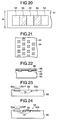
- Figs. 11-13 illustrate a fifth embodiment directed to a construction of a photodetector.
- the photodetector includes light receiving areas surrounded by non-light receiving area.
- the photodetector has two aluminum layers that serve to block light from reaching the non light receiving area.
- Figs. 11-13 are fragmentary view of the non light-receiving area formed in the photodetector.
- a silicon substrate 21 has an interlayer dielectric 22 formed thereon.
- a first aluminum layer 23 for the purposes of wiring and blocking light.
- Another interlayer dielectric 24 is formed on the first aluminum layer 23.
- a second aluminum layer 25 is formed on the interlayer dielectric 24, the second aluminum layer 25 extending over a large area as shown in Fig. 11 for blocking the incident light.
- the first aluminum layer 23 is electrically connected to the second aluminum layer 25.
- Through-holes 26 are formed in the second aluminum layer 25 and a protecting film 27 is formed on the top of the second aluminum layer 25.
- the through-holes 26 are arranged in a checker board pattern as shown in Fig. 11.
- the through-holes 26 may be arranged in patterns different from the checker board pattern as long as they are disposed at 10-30 ⁇ m intervals.
- the interlayer dielectric 22 and 24 are the same as that usually formed during element forming process in the manufacture of C-MOSs and bipolar transistors.
- the shape of the through-holes 26 is not limited to a square but can be of other shapes such as a rectangle.
- the through-holes may be arranged alternately with the second aluminum layer 25' and may extend straight as indicated at 26' in Fig. 13.
- the second aluminum layer 25 is flat and is simply deposited on the interlayer dielectric (oxide). Therefore, the second aluminum layer 25 may come off the interlayer dielectric due to laterally exerted forces, for example, when a resin is applied for sealing against environment.
- Through-holes are very effective in that the second layer of aluminum projects into the through-holes to firmly hold the interlayer dielectric 24. This construction permits the second aluminum layer 25 to resist a laterally exerted force that tends to peel off or slide the second aluminum layer 25.
- Figs. 14-17 illustrate a sixth embodiment directed to a construction of a photodetector.
- the sixth embodiment differs from the fifth embodiment in that contact holes 34 are formed in the first interlayer dielectric 32 in addition to the through-holes.
- Reference numeral 35 denotes an interlayer dielectric and reference numeral 38 denotes a protective layer.
- the contact holes 34 are also arranged in a similar manner to the through-holes 26 in the fifth embodiment.
- the sizes of the contact holes 34 and through-holes 37 are, for example, 10 ⁇ m square in this embodiment but are not important.
- the contact holes 34 and through-holes 37 should preferably be densely arranged for sufficient mechanical strength.
- Fig. 14 illustrates an example of the arrangement of the contact holes 34 and through-holes 37 where the through-holes 37 are aligned in a row and the contact holes 34 are aligned in an adjacent row, each contact hole 34 being between the through-holes 37 in the adjacent row.
- Fig. 16 illustrates another example of the arrangement where the through-holes 37 are disposed alternately with the contact holes 34 in each row, the contact holes 34 being adjacent to the through-holes 37 in the adjacent row.
- the shapes of the through-holes 37 and contact holes 34 are not limited to a square but may be, for example, a rectangle.
- the contact holes 34 may extend straight as indicated at 34' in Fig. 17.
- the reference numeral 36' denotes a second aluminum layer and is electrically connected to the first aluminum layer 33.
- Forming the contact holes 34 in the first aluminum layer 33 increases "holding effect" as shown in Fig. 15 so that the first aluminum layer 33 firmly holds the substrate, resisting laterally exerted forces that tend to peel off or slide the first aluminum layer.
- the holding effect of the first aluminum layer 33 allows the second aluminum layer 36 to further resist laterally exerted forces.
- Figs. 18-19 illustrate a seventh embodiment directed to a construction of a photodetector.
- a polysilicon layer 43 is formed around contact holes 42 in a carrier absorbing area of a photodetector 41.
- This polysilicon layer 43 is usually formed during gate-forming process of the C-MOS semiconductor manufacturing process. While the contact holes 42 are surrounded by the continuous polysilicon layer 43, the contact holes 42 may be surrounded by separate polysilicon layers 43a as shown in Fig. 19.
- the pattern ratio of polysilicon i.e., the ratio of the area occupied by the polysilicon to the total chip area is extremely small with the result that the chips (wafer) are not processed reliably and their characteristics vary from chip to chip if the chips are manufactured through wafer process in which IC chips having ordinary signal processing circuits are manufactured.
- Inserting a polysilicon layer into a space between the light receiving areas increases the pattern ratio of polysilicon to the total chip area, ensuring the reliable processing of the wafer.
- Arranging the polysilicon layer to surround the contact holes or through-holes causes uneven shapes similar to those shown in Fig. 15. Such uneven shapes allow the first and second aluminum layers formed over a large area for the purpose of light-blocking to firmly hold the layer thereunder, the aluminum layers withstanding forces that tend to laterally slide or peel off the aluminum layers.
- Figs. 20-24 illustrate an eighth embodiment directed to a construction of a photodetector.
- Arranged between the adjacent light-receiving areas 52 are carrier absorbing areas 53 in which contact holes 54 are formed as shown in Fig. 21.
- the carrier absorbing areas 53 do not contribute to the output of the light-receiving chips 51.
- a diffusion layer 66 is formed in the carrier absorbing area 53 and contact holes 54 are formed in an interlayer dielectric 67 over the diffusion layer 66.
- the shape of the diffusion layer 66 is not limited to a square and may be other shapes such as a rectangle or even a straight belt-like shape.
- An aluminum layer 68 is formed on the interlayer dielectric 67, filling the contact holes 54.
- the aluminum layer 68 is connected to the potential of a power supply or ground.
- the aluminum layer 68 is covered with a protective layer 69 that protects the photodetector from the environment.
- the photodetector operates as follows: Referring to Fig. 23, when light impinges the light-receiving area 52a, carriers are generated in the light-receiving area 52a. Majority of the generated carriers is absorbed through the electrode, not shown, connected to the light-receiving area 52a, becoming a photocurrent. However, some 70 of the carriers migrate to the adjacent light-receiving area 52b on which no light impinges, and are absorbed through the electrode of this adjacent light-receiving area 52b. As a result, a photocurrent flows through the electrode of the adjacent light-receiving area 52b even though no light is incident upon the adjacent light-receiving area 52b.
- the contact holes 54 serve to absorb carriers migrating from one light-receiving area 52a to the other 52b before the carriers reach the adjacent light receiving area 52b as shown in Fig. 24, thereby preventing the carriers from reaching the adjacent light-receiving area 52b.
- This carrier absorbing effect eliminates an unwanted output of the light-receiving area 52b when light is not incident thereon, maintaining a sufficiently lower, dark level of the output.
- a ninth embodiment is directed to the arrangement of the light-emitting elements.
- Fig. 25 illustrates all the LED chips 76 arranged at 3 mm intervals on an LED board 75.
- Fig. 26 illustrates the distribution of the amount of light emitted from the LED chips 76. The distribution is plotted along the LED board 75, curve 77 representing the amount of light emitted from each LED chip and curve 78 showing the overall distribution of the amount of light.
- Fig. 27 illustrates LED chips 72a, 72b, and 72 arranged longitudinally of an LED board 71 and Fig. 28 illustrates the distribution of the light emitted from the light-emitting elements. The distribution is plotted along the LED board 71, curve 73 representing the distribution of the amount of light emitted from the respective LED chips and curve 74 showing the overall distribution.
- the LED chips 72b-72g are all arranged at predetermined intervals L but the LED chip 72a and the LED chip 72b are spaced apart a shorter distance L1 than the other LED chips.
- the LED chips 72a and 72b are 1.7 mm apart and the other LED chips are 3 mm apart.
- More than two chips may be closely arranged than the other chips depending on a desired contour of the distribution 74 of the amount of emitted light, especially the "shoulder" of the distribution curve 74. If the LED chips are arranged still closer at the end of the arrangement, the shoulder of the distribution curve becomes steeper.
- a tenth embodiment is directed to the arrangement of the light-emitting elements.
- Fig. 29 illustrates LED chips arranged longitudinally of an LED board 71 and Fig. 30 illustrates the distribution of the amount of light emitted from the LED chips 72a-72g, the distribution being plotted along the LED board 71.
- arranging the LED chip 72a closer to the LED chip 72b improves the flatness of curve 74 near its shoulder but results in a hump 74a. This is due to the fact that the light emitted from the first to fourth LEDs 72a-72d are added together. The skirt of the hump 74a reaches over the third LED chip 72c.
- the LED chips disposed closer to the center of the LED board 71 than the LED chip 72c are spaced apart by a predetermined distance L, while the first and second LEDs 72a and 72b are spaced apart by a distance L2 shorter than the predetermined distance L, and the second and third LEDs 72b and 72c are spaced apart by a distance L3 longer than the predetermined distance L.
- the distances L2, L3, and L are 1.7 mm, 5 mm, and 3 mm, respectively.
- the LED chips may be arranged as shown in Fig. 31.
- the first and second LED chips 72a and 72b are spaced apart by a distance L4 and the third and fourth LED chips 72c and 72d are spaced apart by a distance L5, L4 and L5 being sufficiently shorter the distance L (equal pitch).
- the second and third LED chips 72b and 72c are spaced apart by a distance L5 slightly shorter than the distance L.
- the fourth and fifth LED chips 72d and 72e are spaced apart by a distance L7 longer than the distance L.
- the distances L4 and L6 are 1.7 mm, and the distances L5, L7, and L8 are 3, 5, and 4 mm, respectively.
- Curve 74 shown in Fig. 30 loses its flat part by the amount of the hump 74a, which is determined by the resultant distribution of light emitted from the equally spaced LED chips and the LED chips more closely spaced than the equally spaced LED chips.
- the hump 74a of curve 74 may be reduced by arranging the LED chips such that the group of the closely located LED chips are away from the group of the equally spaced LED chips, by a distance longer than the interval of equally spaced LED chips.
- the drive currents of the LED chips may be varied such that the closely arranged LED chips are supplied with less currents than the LED chips arranged at the predetermined intervals, thereby providing substantially flat overall distribution of light.
- An eleventh embodiment is also directed to the arrangement of light emitting elements.
- some LED chips near the longitudinal end of the LED board are not aligned in line with the rest of the LED chips.
- LED chips 82a, 82b, and 82 are die-bonded on a glass epoxy board 81.
- the two LED chips 82a and 82b are obliquely arranged and offset from the center line A-B, the chip 82a being on one side of the line A-B and the chip 82b on the other.
- the LED chips 82a and 82b are, for example, a distance less than 1 mm away from the line A-B.
- the distance L8 between the LED chips 82a and 82b is shorter than the distance L, and the distance L9 between the LED chips 82b and the third chip 82 is longer than the distance L.
- the LED chips 82a and 82b may be disposed oppositely across the line A-B as shown in Fig. 33.
- LED chips 82a and 82b While only two irregularly arranged LED chips 82a and 82b are illustrated in Figs. 32 and 33, a larger number of LED chips may be arranged in a similar manner. Groups of different number of LED chips may be differently arranged at different locations as shown in Fig. 34, the LED chips being differently spaced apart both longitudinally and laterally of the LED board 81.
- the LED chip 82b is on the center line A-B.
- the LED chips 82a and 82c are offset from the center line A-B by distances L11 and L12, respectively, and longitudinally away from the LED chip 82b by distances L13 and L14, respectively.
- the LED chips 82c and 82d are spaced apart by a distance L17 longitudinally of the LED board 81.
- the chips 82d-82e are offset from the center line A-B by distances L15 and L16, respectively, and are spaced apart longitudinally by a distance L18.
- the eleventh embodiment solves the problem shown in Fig. 28 that if the LED chips are equally spaced, the overall distribution of the amount of light emitted from the LED chips decreases below its flat part toward the end of the LED board 81.
- a twelfth embodiment is directed to means (lens 93) for guiding the light emitted from LED chips toward an original to be read.
- Fig. 35 illustrates a construction of an optical read sensor.
- an LED board 91 is mounted obliquely in a case 97 and has LED chips 92 mounted thereon.
- a lens 93 is obliquely mounted above the LED chip 92 and directs the light emitted from the LED chip 92 toward an original placed on a glass cover 94.
- the lens 93 is a lens that has no focal point on the downstream side thereof and converts the light emitted from the LED chips 92 into a beam 98 of substantially parallel light.
- the lens 93 is formed of a transparent resin and has an aspherical surface so that the lens 93 has a negligible aberration and caustic curves.
- the lens 93 projects a beam of light that crosses center line K-K' of the SLA 95 at a point P above the glass cover 94.
- the point is a distance L opt above the original 99 placed on the glass cover 94.
- the lens 93 is very effective in collimating the light from a light source.
- the light through the lens 93 illuminates white paper placed on the top surface of the glass 94 and the light is reflected by the paper to a photodetector 96.
- the output of the photodetector 96 is about more than twice that when the lens 93 is not used.
- the beam 98 of light has a substantially uniform distribution of intensity in an area directly above the SLA 95, i.e., an area in which the original is to be read.
- the light is reflected by the original 99.
- the reflected light passes through the SLA 95 and is incident upon the photodetector 96.
- the original 99 travels forward in a direction shown by arrow M while slightly moving up and down. Therefore, if the distance L opt is somewhat wider than the maximum vertical movement of the original 99, the amount of reflected light remains substantially the same regardless of the vertical movement of the original 99.
- a thirteenth embodiment is directed to a construction of a reflector used in combination with LED chips.
- Fig. 38 illustrates a reflector 103 according to the thirteenth embodiment.
- LED chips 102 are arranged on an LED board 101 longitudinally thereof.
- the LED board 101 takes the form of a glass epoxy board.
- a reflector 103 has upwardly inclined side walls so that the reflector 103 has a larger opening with increasing distance from the LED board.
- the reflector 103 is mounted on the LED board 101, isolating adjacent LED chips from one another.
- the side walls are inclined by approximately 50 degrees with respect to the surface of the glass epoxy board.
- Fig. 39 illustrates another reflector 107 which separates groups of three adjacent LED chips 106 one group from another.
- the reflectors 103 and 107 serve to reduce interference between the light emitted from the respective groups so as to render the resultant distribution of light more uniform.
- a fourteenth embodiment is also directed to the specific construction of a reflector.
- Fig. 40 is a top view of the reflector 107 and Fig. 41 is a cross-sectional view taken along the line A-A' of Fig. 40.
- Fig. 42 is a cross-sectional view when the reflector 107 is mounted on the LED board, showing the bridges 107a that separate groups of three adjacent LED chips 106 from one another.
- the bridges 107a may be formed to separate the adjacent LED chips from one another.
- the minimum height of the bridge 107a is determined depending on the conditions of the resin-molding process of the reflector 107. Referring to Fig. 40, the height of bridges 107a of the reflector 107 is selected to be less than 0.5 mm. In the fourteenth embodiment, the height is 0.4 mm.
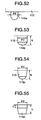
- a fifteenth embodiment is directed to a mounting construction of a reflector.
- Fig. 48 shows a reflector 112 of the invention fixedly mounted to an LED board 111 in a conventional manner where the legs of the reflector 112 are deformed by melting at a portion 114 by heat.
- the LED board 111 is in the form of a glass epoxy board.
- a problem with the conventional manner of fixing the reflector to the LED board 111 is that the reflector 112 may be raised slightly from the LED board 111 when the legs are melted by pressing a heater from the reverse side of the LED board 111.
- an exclusive assembly jig is needed to melt the end of the legs.
- Fig. 49 is an enlarged fragmentary perspective view, illustrating a fifteenth embodiment.
- the legs 113 are L-shaped and is formed in one piece construction with the reflector 112.
- the length N of the leg 113 is selected in accordance with the thickness of the LED 111, i.e., the effective length N of the legs 113 is the same as the thickness of the LED board 111.
- the reflector 112 is fixedly mounted by inserting the legs 113 through openings 111a formed in the LED board 111 as shown in Fig. 50.
- Fig. 51 is a cross-sectional view taken along lines XVIII-XVIII in Fig. 49.
- the legs 113 When the legs 113 are pushed into the openings, the legs 113 are somewhat resiliently deformed yieldably toward each other as depicted by arrows shown in Fig. 51 and the hooks 113a snap out of the openings 111a after the hooks completely pass through the openings 111a.
- the leg 113 having the hook 113a in one piece construction allows press-fit assembly operation, eliminating the use of an exclusive assembly jig. This construction prevents the reflector from being raised from the LED board 111.
- the hooks 113a may be a variety of shapes such as those shown in Figs. 52-55.
- Fig. 52 shows a cylindrical leg 115a with a round end
- Fig. 53 shows a cylindrical leg 115 with a partially spherical end 115b
- Fig. 54 shows a leg in the form of a truncated cone having a partially spherical end 115c
- Fig. 55 shows a cylindrical leg with a truncated cone 115d.
- the legs shown in Figs. 52-55 are press-fitted into holes formed in the LED board.
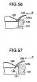
- a sixteenth embodiment is directed to a guiding construction for guiding an original onto a glass cover.
- the glass cover 122 is laterally held by projections 125 and 127 as shown in 20C.
- an original 126 to be read is fed in a direction shown by arrow R.
- the original 126 is apt to be caught at its front edge by a gap 124a between the glass cover 122 and a case 123 as shown in Figs. 56 and 57.
- the gaps 124a may be eliminated by providing guides 125a as shown in Fig. 59.
- the guide 125a has a round upper end and projects upwardly higher than the adjacent surface of the glass cover 122 and is flush with the upper edge of the case 123. When the original 126 is fed, it is smoothly guided by the round upper end of the guide 125a to smoothly ride onto the beveled surface of the glass cover 122.
- the gap 124b may be eliminated by providing guides 127a as shown in Fig. 59.
- the guide 127a has an upper end which is a distance ⁇ d below the top surface of the glass 122, so that the original 126 is smoothly discharged out of the read sensor.
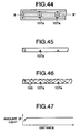
- a seventeenth embodiment is directed to a manner in which an SLA is fixed to a case of a read sensor.
- Figs. 60-63 illustrate the seventeenth embodiment.
- An SLA 131 is the same construction as the prior art SLA 203 shown in Figs. 77 and 78.
- Each of the fibers in the SLA 131 has two focal points; one is on the light incident side thereof and the other is on the light emerging side.
- the resolution of data read from the original critically varies depending on whether one of the focal points of the SLA is on the original and the other on the light-receiving surfaces of the photodetectors. Poorly focusing on any of the original and light sensors results in poor resolution of the data.
- the SLA 131 is conventionally fixedly mounted to a wall 132 of a case by applying a resin 133 to the wall 132 of the case 141 and then pressing the SLA 131 against the wall 132 to which the resin 133 is applied.
- This mounting method presents a problem that when the SLA 131 is pressed onto the wall 132, an excess portion 133' of the resin 133 spreads and the excess resin can reach the light incident ends of the optical fibers as shown in Fig. 61.
- a case 141 is formed with a semi-cylindrical groove 134 in the wall 132 as shown in Fig. 62, the groove 134 having a diameter of about 0.5 mm and extending in a direction perpendicular to the page of Fig. 62.
- the groove 134 is filled with silicone resin 135 and the SLA 131 is firmly pressed against the wall 132 as shown in Fig. 63. Some of the silicone resin 135 may spread into a gap between the SLA 131 and the wall 132 but will not come out of the gap.
- the groove 134 may be other shapes such as a rectangular column. While a single groove 134 is formed in the wall 132 shown in Figs. 62 and 63, a plurality of grooves may be formed for increased adhesion.
- Fig. 64 shows an eighteenth embodiment which is directed to a manner in which an SLA 131 is fixed to a case 141.
- a plurality of laterally extending holes 142 are formed in a case 141 which is made by extruding aluminum. Three holes 142 per 80 mm distance are sufficient.
- the holes 142 have a diameter of about 1 mm and the resin is poured into holes 142 from a direction shown by D for securely bonding the SLA 131 to the case 141.
- FIG. 65 is a cross-sectional side view with a partial sectional view, illustrating a mounting construction where an SLA 151 is mounted to a case 152.
- Fig. 66 is a perspective cross-sectional view.
- the case 152 has a generally L-shaped holder 156 and an obliquely downwardly extending holder 158 on which an LED board 157 is mounted.
- the holder 158 is made of a material such as polycarbonate plastics.
- the holder 158 has hemispherical projections 155 and the L-shaped holder 156 has an upper retaining hook 153 and a lower retaining hook 154.
- the upper and lower retaining hooks 153 and 154 are spaced apart just enough for the SLA 151 to snugly fit therebetween.
- the hemispherical projections 155 are somewhat yieldably deformed, pressing the SLA 151 against the L-shaped holder 156 to firmly hold the SLA 151.
- a twentieth embodiment is directed to a mounting construction of an LED board 163 in the form of a glass epoxy board.
- Fig. 67 is a perspective view of a case to which the LED board 163 is assembled and Fig. 68 is a top view of the construction in Fig. 67.
- a case 160 is formed with two pairs 161 and 162 of mounting projections.
- Each pair 161 or 162 includes two mounting projections 161a-161b or 162a-162b arranged back-to-back with a slot 161c or 162c therebetween.
- the slot 161c extends in a direction shown by arrows E-E' while the slot 162c extends in a direction shown by arrows F-F' perpendicular to the direction shown by arrow E-E'.
- Each pair is generally cylindrical and projects upward from the bottom of the case 160.
- the mounting projections 162a and 162b each have a hook 162d which is formed at its free end and projects diametrically outwardly.
- the LED board 163 has LED chips, not shown, mounted thereon and two round holes 164a and 164b formed therein.
- the LED board 163 is first held horizontally above the case 160 and then lowered so that the pairs 162 and 161 extend into the round holes 164a and 164b, respectively.
- the mounting projections 162a and 162b arranged back-to-back are yieldably deformed toward each other.
- the mounting projections 161a and 161b arranged back-to-back are yieldably deformed toward each other.
- the two pairs 161 and 162 of mounting projections deform in directions perpendicular to each other.
- the hooks 162d snap out of the holes 164a and 164b, regaining their original positions to firmly hold the LED board 163 between the hooks 162d and the bottom surface 161a of the case 160.
- the LED board 163 Upon assembling the LED board 163 to the case 160, the LED board 163 is securely held both horizontally and vertically.
- the round holes 164a and 164b formed in the LED board 163 have a diameter of 2 mm and the hooks 162d project 0.4 mm diametrically outwardly to engage the LED board 163.
- the LED board 163 may be formed with elongated holes 165a and 165b as shown in Fig. 72 in place of the round holes 164a and 164b.
- the elongated holes 165a and 165b are 2 mm in diameter and 5 mm in length, and extend perpendicular to each other, the centers of the holes being symmetrical about the center line G-G' of the LED board 163.
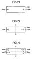
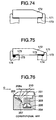
- Four elongated holes in stead of two holes may be arranged as shown in Fig. 73, the holes 165a-165b and the holes 165c-165d being symmetrical about the center line G-G', respectively, while the holes 165a and 165c and the holes 165b and 165d being symmetrical about the center line H-H'.
- a larger number of elongated holes may of course be arranged in order to more securely mount the LED board 163.
- the pairs 161 and 162 of mounting projections 161a-161b and 162a-162b prevent the LED board 163 from moving in the direction perpendicular to the direction in which the elongated holes extends but does not prevent from moving in the direction in which the elongated holes extend. Therefore, the slots 161c and 162c are formed to extend in the same direction as the elongated holes, so that the pairs of mounting projections resiliently push the LED board 163 in a direction perpendicular to the direction in which the elongated holes 165a-165d extend, thereby securely holding the LED board 163 once the LED board 163 is assembled to the case 160.
- a twenty-first embodiment is directed to a mounting construction of glass cover 172 on which an original to be read is placed.
- the glass cover 172 is fixed to the case 171 by a silicone resin 173.
- the silicone resin 173 was conventionally applied to flat surfaces of the case 171.
- the layer of the silicone resin 173 is very thin after the glass 172 is bonded to the case 171, resulting in decreased adhesion.
- the thin layer of the silicone resin 173 can cause some gaps to develop between the glass 172 and the case 171 through which dust and moisture may enter, resulting in denatured silicone resin.
- the case 171 is formed with grooves 174 therein, which holds an adhesive therein.
- the grooves are 0.5 to 1 mm wide and 0.5 mm deep.
- the groove 174 holds a sufficient amount of adhesive between the case 171 and glass cover 172, providing sufficient adhesion as well as eliminating the gap which would develop if the layer of the adhesive 173 is too thin. In other words, the groove 174 offers some sealing effect.
Abstract
An optical read sensor includes a circuit board (1, 71,
75, 81) having light-emitting elements (3, 72a-72g, 76, 92,
106) mounted thereon, transparent cover (6, 94, 122, 172) on
which an original (99, 126) to be read is placed, light-receiving
elements (96), and light-guide (7, 95, 131, 151)
that guides the light reflected by the original (99, 126) to
the light-receiving elements (9a, 96). The light-emitting
elements (3) emit light toward the original (99). The
original (99) reflects the light emitted from the light-emitting
elements through the transparent cover (6). The
light guide guides (7, 95, 131, 151) the light reflected by
the original (99) to the light-receiving elements (9a, 96).
Description
The present invention relates to an optical sensor for
reading a pattern on an original.
Figs. 76-78 illustrate a conventional optical sensor
for reading a pattern from an original. Referring to Fig.
76, a glass cover 201 is placed on a frame 202. An original
210 to be read travels over the glass cover 201 in a
direction shown by arrow Q. An LED board 207 is mounted
obliquely in the frame 202. The LED board 207 has current
limiting resistors, not shown, and LEDs 206 mounted thereon.
Arranged at the bottom of the frame is a photodetector board
204 on which photodetectors 205 are mounted. A SELFOC lens
array (referred to as SLA hereinafter) 203 is mounted
between the glass cover 201 and photodetector board 204.
"SELFOC lens" is a trade name. The SELFOC lens array is
formed of a plurality of optical fibers arranged parallel in
a row. Each of the optical fibers has a focal point on the
light incidence side and another focal point on the light
exiting side. The SLA 203, photodetector board 204, and LED
board 207 extend in directions perpendicular to the page of
Fig. 76.
The light 206a emitted from the LEDs 206 illuminates
the original 210 on which a pattern is printed. The light
206a is randomly reflected by the original 210 and some of
the reflected light passes through the glass cover 201 and
SLA 203 to the photodetectors 205 which detect the pattern
printed on the original 210. Fig. 77 is a fragmentary
perspective view of the SLA 203 and Fig. 78 is a cross-sectional
view thereof showing focal points f1 and f2. The
SLA 203 is of the construction in which a plurality of
optical fibers 208 are aligned in array form integrally
assembled in resin body 209. The SLA 203 has a focal point
f1 on its light incident side and a focal point f2 on its
light-emerging side, the two focal points being spaced apart
by a distance Tc. The focal points f1 an f2 of the SLA 203
are symmetrical with respect to the center line C-C' but may
shift, after the SLA 203 is assembled into the sensor, if
the optical path includes a component(s) made of a material
such as plastics or glass having a refractive index
different from that of air. The diameter of the optical
fibers 208 determines the resolution of the SLA 203 which in
turn determines the minimum thickness of lines and minimum
size of a black-and-white pattern that can be read from the
original.
The photodetector 205 is a line sensor in which light-receiving
areas are aligned at, for example, intervals of 1
dot/mm, 2 dot/mm, 8 dot/mm, or 16 dot/mm. The total length
of the row of the photodetectors 205 determines the width of
a pattern that can be read from the original 210.
The information on an original is read on a line-by-line
basis and therefore each line must be illuminated by
the light having the same intensity across the line. In
order that the outputs of the photodetectors correctly
represent black and white levels of the original, the same
amount of light must illuminate across the area on the
original being read and the photodetectors must receive only
the light reflected by the original. However, with the
aforementioned prior art read sensor, some of the light 206a
emitted from the LEDs 206 may leak through the LED board
into the photodetectors 205 or may illuminate the
surroundings of the photodetectors 205 so that the light
reflected by the surroundings enters the photodetectors 205.
Such unwanted light causes the outputs of the photodetectors
205 to increase, resulting in a smaller difference between
the white level and black level. In other words, unwanted
light results in a poor signal to noise ratio of the output
of the sensor 210, hence a smaller dynamic range of the
sensor output.
A poor signal to noise ratio of the output of the
photodetector 205 causes different sensor outputs depending
on locations on the line being read when reading an original
having the same reflectivity across the line.
The desired overall resolution of data cannot be
obtained if the LEDs 206 are not properly oriented to emit
light in the right direction and/or the SLA 203 and
photoreceptor 205 are not assembled exactly at the designed
locations. In addition, the read sensor is subjected to a
considerable amount of vibration when the apparatus is
actually operated and therefore the LEDs 206, SLA 203, and
photodetectors 205 must be securely mounted so that the
vibration does not change their relative positions.
Conventionally, the LEDs 206, SLA 203 and photodetectors 205
are fixed by an adhesive. However, adhesion is not
sufficient to accurately and securely mount the LEDs 206,
SLA 203, and photodetectors 205.
An object of the present invention is to provide a read
sensor for optically reading a pattern on the original, the
read sensor offering a desired resolution and having an
improved mechanical strength.
An optical read sensor according to the invention
includes an LED board (1, 71, 75, 81) having light-emitting
elements (3, 72a-72g, 76, 92, 106) mounted thereon,
transparent cover (6, 94, 122, 172) on which an original
(99, 126) to be read is placed, light-receiving elements
(9a, 51, 96), and light-guide (7, 95, 131, 151) that guides
the light reflected by the original to the light-receiving
elements (9a, 96).
The light-emitting elements (3, 72a-72g, 76, 92, 106)
emit light toward the original (99, 126). The original (99,
126) reflects the light emitted from the light-emitting
elements (3, 72a-72g, 76, 92, 106) through the transparent
cover (94, 122, 172). The light guide (7, 95, 131, 151)
directs the light reflected by the original (99, 126) to the
light-receiving elements (9a, 51, 96). The light-receiving
elements (9a, 51, 96) receive the light reflected by the
original (99, 126) through the transparent cover (6).
Leakage of the light emitted from the light-emitting
elements (3) is minimized by the bonding pads (2) extending
over substantially the entire the LED board (1). The
smaller size of the LED board (1) can be accomplished by
forming wire patterns (5b) on the back side of the LED board
(1) and current limiting resistors (5) for limiting currents
through the light-emitting elements (3) are mounted on the
wire patterns (5b).
The bonding pad (2) may be formed to have a wire
bonding pad (14) and a die bonding pad (13) connected by a
narrow conductor path (12a).
The light receiving element (9a, 51, 96) has a light-blocking
area (25) which surrounds light-receiving areas
(26). The light-blocking area (25) is of an uneven surface
structure so that the light-blocking layer firmly holds the
semiconductor substrate (21). The light receiving element
(96) may have carrier absorbing electrodes (54) formed
between adjacent light-receiving areas (52a, 52b).
In order to obtain light having a uniform distribution
of the amount of light, the light emitting elements (3) may
be arranged at a variety of intervals. The light may be
collimated by a lens (93) or reflected by a reflector (103)
mounted on the LED board (101) toward the original to be
read.
The case (141) may be formed with a groove (134) in
which an adhesive (135) is held between the light guide
(131) and the case (141), thereby firmly holding the light
guide (131) in position. The case may (141) also be formed
with through-holes (142) through which an adhesive is
introduced into the interface between the light guide (131)
and case (141). Upper and lower hooks (153, 154) may be
formed on the wall of the case. The light guide (151) is
held by the hooks (153, 154) in position and engaged with
projections (155) that press the light guide (151) against
the wall (156).
The case (160) may have projections (162) with which
the circuit board (163) is mounted to the case, thereby
firmly positioning the circuit board (163).
Further scope of applicability of the present invention
will become apparent from the detailed description given
hereinafter. However, it should be understood that the
detailed description and specific examples, while indicating
preferred embodiments of the invention, are given by way of
illustration only, since various changes and modifications
within the spirit and scope of the invention will become
apparent to those skilled in the art from this detailed
description.
The present invention will become more fully understood
from the detailed description given hereinbelow and the
accompanying drawings which are given by way of illustration
only, and thus are not limitative of the present invention,
and wherein:
Preferred embodiments of the invention will be
described in detail with reference to the drawings.
Fig. 1 is a fragmentary top view of a light emitting
section of an optical read sensor of a first embodiment.
Referring to Fig. 1, the LED board 1 is in the form of a
glass epoxy circuit board. The die bonding pads 2 are
formed on an LED board 1 by plating copper patterns with
gold and have notches that facilitate positioning of the LED
chips 3 thereon. When the LED chip is to be mounted at a
location other than the central area of the bonding pad 2,
the notches effectively indicate an exact location on the
bonding pad 2 where the LED chip 3 is to be mounted. The
LED chips 3 are die-bonded to the die bonding pads 2. In
this embodiment, the die bonding pads also serve as wire
bonding pads. Each LED chip is electrically connected to
the die bonding pad 2 of the adjacent LED chip by means of
gold wire bond 4, so that the LED chips are connected in
series. The die bonding pad 2 extends over as large an area
as possible on the LED board 1. The die bonding pads 2 are
formed on the LED board 1 by gold-plating during the
manufacture of the LED board 1, and therefore the distance
between the die bonding pads 2 is selected to be usually in
the range of 0.3-0.4 millimeters. The die bonding pads 2
may extend transversely of the LED board 1 to cover almost
the full width of the LED board 1 as long as the die bonding
pads 2 are not short-circuited to each other.
A large surface area of the die bonding pad 2 is
effective in preventing a large portion of the light emitted
from the LEDs from transmitting through the LED board 1.
The surfaces of the gold-plated die bonding pads 2 serve to
effectively reflect the light emitted from the LEDs,
increasing the total amount of light which reaches the
original.
Thus, the first embodiment prevents the leaked light
from entering the photodetectors, thereby solving the
problem that the leaked light increases the output of the
photodetectors when the photodetectors are reading black
patterns.
Figs. 2-4 illustrate a second embodiment of an optical
read sensor. The second embodiment is characterized in that
current limiting resistors are mounted on an LED board 1.
Fig. 2 shows the front side of the LED board 1 on which LED
chips 3 are mounted and the back side on which current
limiting resistors 5 (chip type resistors) are mounted.
Fig. 3 shows an electrical equivalent circuit of Fig. 2.
The LED board 1 takes the form of a glass epoxy board
and has die bonding pads 2 on the front side thereof
connected via a through-hole 2a with wire patterns 5b. The
LED chips 3 are bonded on the die bonding pads 2.
As shown in Fig. 3, the LED chips 3 are wired in series
with the current limiting resistor 5 and the series circuits
are then connected in parallel. The current limiting
resistor 5 may be of a lead type, in which case holes must
be made for inserting the leads of the resistor through the
LED board 1 and therefore the mounting location of the
resistor 5 should be carefully selected so that the leads
are not short-circuited to the other die bond pads 2. The
LED chips 3 and current limiting resistors may be mounted on
the same side of the LED substrate 1, in which case the LED
board 1 should be wider than that shown in Fig. 2.
Fig. 4 is a cross-sectional view of the sensor when
assembled into a frame 10, showing the LED board 1. In this
case, the LED chips 3 and current limiting resistors 5 are
mounted on the same side of the LED board 1. A glass cover
6 on which an original to be read is placed is assembled on
the top of the frame 10. Photodetector board 9 are disposed
on the bottom of the frame 10. Disposed between the glass
cover 6 and the photodetector board 9 is an SLA 7. The SLA
7, LED board 1, and photodetector board 9 extend in
directions perpendicular to the page of Fig. 4. While the
LED chips 3 and the current limiting resistors 5 are mounted
on the same side of the LED board 1, the current limiting
resistors 5 may be mounted on the other side so that the LED
board 1 can be smaller in width. A smaller width of the LED
board 1 is advantageous in miniaturizing the sensor.
The total thickness of the gold-plated pad patterns is
only about several microns and the thickness of the gold is
less than a micron. Therefore, some amount of light emitted
from the LED chips 3 still leaks therethrough. Thus, the
pad pattern 2 may also be provided on the other side of the
LED board 1 to considerably increase the light-blocking
effect. The pad patterns on the both sides of the LED board
1 are gold-plated.
While the die bonding pads 2 extending over
substantially the entire surface of the LED board 1 reflect
a large portion of the light emitted from the LEDs to the
original, some of the light leaks through the die bonding
pads 2 since the die bonding pads 2 are only several microns
thick.
Referring to Fig. 5, wiring patterns 11 are formed on
the back side of the LED board 1. Current limiting
resistors 5 are mounted bridging the two adjacent wiring
patterns 11, and soldered at 5a to the patterns as shown in
Fig. 6.
The die bonding pads 2 on the front side of the LED
board 1 extend over substantially the entire surface of the
LED board 1 as shown in Fig. 5, and the wiring patterns 11
on the back side also extend substantially over the surface
of the LED board 1 as shown in Fig. 6. The die bonding pads
2 and the wiring patterns 11 are arranged in a staggered
relation so that the gap g1 between the die bonding pads 2
do not overlap the gap g2 between the wiring patterns 11.
In this manner, the front side-to-back side leakage of light
can be minimized.
Providing the die bonding pads 2 on one side of the
LED board 1 and patterns of a shape similar to that of the
die bonding pads 2 on the other side and arranging the
patterns in staggered form are advantageous in that light-blocking
effect is improved by a factor of about two as
compared to providing light-blocking patterns only on one
side of the LED board 1, further improving the signal to
noise ratio of the output of the read sensor.
A fourth embodiment is directed to the shapes of the
die bonding pad and wire bonding pad used for an optical
read sensor.
Figs. 7-10 illustrate bonding pads each of which
includes a die bonding pad and a wire bonding pad formed on
the same side of the LED board. Referring to Fig. 7, a
groove 12 is formed to extend so as to define a wire bonding
pad 14 and a die bonding pad 13 connected via a narrow
connection 12a. The width of the groove 12 is in the range
of from 0.3 to 0.4 millimeters depending on the etching
accuracy. The width of the connection 12a also ranges
usually from 0.3 to 0.4 millimeters. The narrow connection
12a effectively prevents the bonding paste applied to the
die bonding pad 13 from spreading into the wire bonding pad
14.
Fig. 8 illustrates the die bonding pad 13 and wire
bonding pad 14 connected together via two connections 12a.
Fig. 9 illustrates the die bonding pad 13 and wire bonding
pad 14 connected via a long connection 12a, in which case a
size of 100 µm square is sufficient for the wire bonding
pad 14. The long, narrow connection 12a effectively
prevents the bonding paste from spreading into the wire
bonding pad 14.
The silver paste used in bonding the LED chip 3 to the
die bonding pad 2 contains a solvent and a resin in liquid
phase. The solvent and resin in liquid phase applied to the
bonding pads 2 spread between the particles of gold on the
gold-plated pad due to capillary phenomenon, decreasing
bonding strength. Defining the die bonding pad 2 and wire
bonding pad 14 by using the groove 12 substantially isolates
the two pads one from the other, preventing the solvent from
spreading into the area of the wire bonding pad 14. The
long connection 12a as shown in Fig. 9 further improves the
isolation effect.
The wire bond pads 14 may be arranged laterally of the
bonding pads 2 as shown in Fig. 10 and connected via
connection 12a to the corresponding bonding pads.
Figs. 11-13 illustrate a fifth embodiment directed to a
construction of a photodetector. The photodetector includes
light receiving areas surrounded by non-light receiving
area. In the fifth embodiment, the photodetector has two
aluminum layers that serve to block light from reaching the
non light receiving area.
Figs. 11-13 are fragmentary view of the non light-receiving
area formed in the photodetector. A silicon
substrate 21 has an interlayer dielectric 22 formed thereon.
Formed on the interlayer dielectric 22 is a first aluminum
layer 23 for the purposes of wiring and blocking light.
Another interlayer dielectric 24 is formed on the first
aluminum layer 23. Then, a second aluminum layer 25 is
formed on the interlayer dielectric 24, the second aluminum
layer 25 extending over a large area as shown in Fig. 11 for
blocking the incident light. The first aluminum layer 23 is
electrically connected to the second aluminum layer 25.
Through-holes 26 are formed in the second aluminum layer 25
and a protecting film 27 is formed on the top of the second
aluminum layer 25. The through-holes 26 are arranged in a
checker board pattern as shown in Fig. 11.
The through-holes 26 may be arranged in patterns
different from the checker board pattern as long as they are
disposed at 10-30 µm intervals. The interlayer dielectric
22 and 24 are the same as that usually formed during element
forming process in the manufacture of C-MOSs and bipolar
transistors. The shape of the through-holes 26 is not
limited to a square but can be of other shapes such as a
rectangle. The through-holes may be arranged alternately
with the second aluminum layer 25' and may extend straight
as indicated at 26' in Fig. 13.
If the through-holes 26 are not formed, the second
aluminum layer 25 is flat and is simply deposited on the
interlayer dielectric (oxide). Therefore, the second
aluminum layer 25 may come off the interlayer dielectric due
to laterally exerted forces, for example, when a resin is
applied for sealing against environment. Through-holes are
very effective in that the second layer of aluminum projects
into the through-holes to firmly hold the interlayer
dielectric 24. This construction permits the second
aluminum layer 25 to resist a laterally exerted force that
tends to peel off or slide the second aluminum layer 25.
Figs. 14-17 illustrate a sixth embodiment directed to a
construction of a photodetector. The sixth embodiment
differs from the fifth embodiment in that contact holes 34
are formed in the first interlayer dielectric 32 in addition
to the through-holes. Reference numeral 35 denotes an
interlayer dielectric and reference numeral 38 denotes a
protective layer. The contact holes 34 are also arranged in
a similar manner to the through-holes 26 in the fifth
embodiment. The sizes of the contact holes 34 and through-holes
37 are, for example, 10 µm square in this embodiment
but are not important. The contact holes 34 and through-holes
37 should preferably be densely arranged for
sufficient mechanical strength.
Fig. 14 illustrates an example of the arrangement of
the contact holes 34 and through-holes 37 where the through-holes
37 are aligned in a row and the contact holes 34 are
aligned in an adjacent row, each contact hole 34 being
between the through-holes 37 in the adjacent row. Fig. 16
illustrates another example of the arrangement where the
through-holes 37 are disposed alternately with the contact
holes 34 in each row, the contact holes 34 being adjacent to
the through-holes 37 in the adjacent row. The shapes of the
through-holes 37 and contact holes 34 are not limited to a
square but may be, for example, a rectangle. The contact
holes 34 may extend straight as indicated at 34' in Fig. 17.
The reference numeral 36' denotes a second aluminum layer
and is electrically connected to the first aluminum layer
33.
Forming the contact holes 34 in the first aluminum
layer 33 increases "holding effect" as shown in Fig. 15 so
that the first aluminum layer 33 firmly holds the substrate,
resisting laterally exerted forces that tend to peel off or
slide the first aluminum layer. Thus, the holding effect of
the first aluminum layer 33 allows the second aluminum layer
36 to further resist laterally exerted forces.
Figs. 18-19 illustrate a seventh embodiment directed to
a construction of a photodetector.
Referring to Fig. 18, a polysilicon layer 43 is formed
around contact holes 42 in a carrier absorbing area of a
photodetector 41. This polysilicon layer 43 is usually
formed during gate-forming process of the C-MOS
semiconductor manufacturing process. While the contact
holes 42 are surrounded by the continuous polysilicon layer
43, the contact holes 42 may be surrounded by separate
polysilicon layers 43a as shown in Fig. 19.
The light-receiving areas occupy most of the chip area
and signal processing circuit uses only 10 to 20% of the
total area. Therefore, the pattern ratio of polysilicon,
i.e., the ratio of the area occupied by the polysilicon to
the total chip area is extremely small with the result that
the chips (wafer) are not processed reliably and their
characteristics vary from chip to chip if the chips are
manufactured through wafer process in which IC chips having
ordinary signal processing circuits are manufactured.
Inserting a polysilicon layer into a space between the
light receiving areas increases the pattern ratio of
polysilicon to the total chip area, ensuring the reliable
processing of the wafer. Arranging the polysilicon layer to
surround the contact holes or through-holes causes uneven
shapes similar to those shown in Fig. 15. Such uneven
shapes allow the first and second aluminum layers formed
over a large area for the purpose of light-blocking to
firmly hold the layer thereunder, the aluminum layers
withstanding forces that tend to laterally slide or peel off
the aluminum layers.
Figs. 20-24 illustrate an eighth embodiment directed to
a construction of a photodetector. Referring to Fig. 20,
the light-receiving chip 51 is about W=1.5 mm wide and has
light receiving areas 52 aligned longitudinally thereof.
Arranged between the adjacent light-receiving areas 52 are
carrier absorbing areas 53 in which contact holes 54 are
formed as shown in Fig. 21. The carrier absorbing areas 53
do not contribute to the output of the light-receiving chips
51. As shown in Fig. 22, a diffusion layer 66 is formed in
the carrier absorbing area 53 and contact holes 54 are
formed in an interlayer dielectric 67 over the diffusion
layer 66. The shape of the diffusion layer 66 is not
limited to a square and may be other shapes such as a
rectangle or even a straight belt-like shape. An aluminum
layer 68 is formed on the interlayer dielectric 67, filling
the contact holes 54. The aluminum layer 68 is connected to
the potential of a power supply or ground. The aluminum
layer 68 is covered with a protective layer 69 that protects
the photodetector from the environment.
If the contact holes 54 are not formed in the carrier
absorbing areas 53, the photodetector operates as follows:
Referring to Fig. 23, when light impinges the light-receiving
area 52a, carriers are generated in the light-receiving
area 52a. Majority of the generated carriers is
absorbed through the electrode, not shown, connected to the
light-receiving area 52a, becoming a photocurrent. However,
some 70 of the carriers migrate to the adjacent light-receiving
area 52b on which no light impinges, and are
absorbed through the electrode of this adjacent light-receiving
area 52b. As a result, a photocurrent flows
through the electrode of the adjacent light-receiving area
52b even though no light is incident upon the adjacent
light-receiving area 52b.
If the contact holes 54 are formed between the adjacent
light-receiving areas 52a and 52b, the contact holes 54
serve to absorb carriers migrating from one light-receiving
area 52a to the other 52b before the carriers reach the
adjacent light receiving area 52b as shown in Fig. 24,
thereby preventing the carriers from reaching the adjacent
light-receiving area 52b. This carrier absorbing effect
eliminates an unwanted output of the light-receiving area
52b when light is not incident thereon, maintaining a
sufficiently lower, dark level of the output.
A ninth embodiment is directed to the arrangement of
the light-emitting elements.
Fig. 25 illustrates all the LED chips 76 arranged at 3
mm intervals on an LED board 75. Fig. 26 illustrates the
distribution of the amount of light emitted from the LED
chips 76. The distribution is plotted along the LED board
75, curve 77 representing the amount of light emitted from
each LED chip and curve 78 showing the overall distribution
of the amount of light.
It is to be noted that the curve 78 falls below the
flat part near the leftmost LED chip as shown in Fig. 26.
Fig. 27 illustrates LED chips 72a, 72b, and 72 arranged
longitudinally of an LED board 71 and Fig. 28 illustrates
the distribution of the light emitted from the light-emitting
elements. The distribution is plotted along the
LED board 71, curve 73 representing the distribution of the
amount of light emitted from the respective LED chips and
curve 74 showing the overall distribution.
Referring to Fig. 27, the LED chips 72b-72g are all
arranged at predetermined intervals L but the LED chip 72a
and the LED chip 72b are spaced apart a shorter distance L1
than the other LED chips. In the embodiment, the LED chips
72a and 72b are 1.7 mm apart and the other LED chips are 3
mm apart.
More than two chips may be closely arranged than the
other chips depending on a desired contour of the
distribution 74 of the amount of emitted light, especially
the "shoulder" of the distribution curve 74. If the LED
chips are arranged still closer at the end of the
arrangement, the shoulder of the distribution curve becomes
steeper.
A tenth embodiment is directed to the arrangement of
the light-emitting elements.
Fig. 29 illustrates LED chips arranged longitudinally
of an LED board 71 and Fig. 30 illustrates the distribution
of the amount of light emitted from the LED chips 72a-72g,
the distribution being plotted along the LED board 71.
Referring back to Figs. 27 and 28, arranging the LED
chip 72a closer to the LED chip 72b improves the flatness of
curve 74 near its shoulder but results in a hump 74a. This
is due to the fact that the light emitted from the first to
fourth LEDs 72a-72d are added together. The skirt of the
hump 74a reaches over the third LED chip 72c.
In the tenth embodiment, as shown in Fig. 29, the LED
chips disposed closer to the center of the LED board 71 than
the LED chip 72c are spaced apart by a predetermined
distance L, while the first and second LEDs 72a and 72b are
spaced apart by a distance L2 shorter than the predetermined
distance L, and the second and third LEDs 72b and 72c are
spaced apart by a distance L3 longer than the predetermined
distance L.
Specifically, the distances L2, L3, and L are 1.7 mm, 5
mm, and 3 mm, respectively.
Alternatively, the LED chips may be arranged as shown
in Fig. 31. The first and second LED chips 72a and 72b are
spaced apart by a distance L4 and the third and fourth LED
chips 72c and 72d are spaced apart by a distance L5, L4 and
L5 being sufficiently shorter the distance L (equal pitch).
The second and third LED chips 72b and 72c are spaced apart
by a distance L5 slightly shorter than the distance L. The
fourth and fifth LED chips 72d and 72e are spaced apart by a
distance L7 longer than the distance L.
In the tenth embodiment, the distances L4 and L6 are
1.7 mm, and the distances L5, L7, and L8 are 3, 5, and 4 mm,
respectively. Curve 74 shown in Fig. 30 loses its flat part
by the amount of the hump 74a, which is determined by the
resultant distribution of light emitted from the equally
spaced LED chips and the LED chips more closely spaced than
the equally spaced LED chips. The hump 74a of curve 74 may
be reduced by arranging the LED chips such that the group of
the closely located LED chips are away from the group of the
equally spaced LED chips, by a distance longer than the
interval of equally spaced LED chips. Further, the drive
currents of the LED chips may be varied such that the
closely arranged LED chips are supplied with less currents
than the LED chips arranged at the predetermined intervals,
thereby providing substantially flat overall distribution of
light.
An eleventh embodiment is also directed to the
arrangement of light emitting elements. In the eleventh
embodiment, some LED chips near the longitudinal end of the
LED board are not aligned in line with the rest of the LED
chips. Referring to Fig. 32, LED chips 82a, 82b, and 82 are
die-bonded on a glass epoxy board 81. The two LED chips 82a
and 82b are obliquely arranged and offset from the center
line A-B, the chip 82a being on one side of the line A-B and
the chip 82b on the other. The LED chips 82a and 82b are,
for example, a distance less than 1 mm away from the line A-B.
The distance L8 between the LED chips 82a and 82b is
shorter than the distance L, and the distance L9 between the
LED chips 82b and the third chip 82 is longer than the
distance L.
Alternatively, the LED chips 82a and 82b may be
disposed oppositely across the line A-B as shown in Fig. 33.
While only two irregularly arranged LED chips 82a and
82b are illustrated in Figs. 32 and 33, a larger number of
LED chips may be arranged in a similar manner. Groups of
different number of LED chips may be differently arranged at
different locations as shown in Fig. 34, the LED chips being
differently spaced apart both longitudinally and laterally
of the LED board 81.
Referring to Fig. 34, the LED chip 82b is on the center
line A-B. The LED chips 82a and 82c are offset from the
center line A-B by distances L11 and L12, respectively, and
longitudinally away from the LED chip 82b by distances L13
and L14, respectively. The LED chips 82c and 82d are spaced
apart by a distance L17 longitudinally of the LED board 81.
The chips 82d-82e are offset from the center line A-B by
distances L15 and L16, respectively, and are spaced apart
longitudinally by a distance L18.
As described above, arranging more LED chips in
proximity to the end of the LED board 81 increases the flat
part of the overall distribution of the amount of light
emitted from the LED chips. Therefore, the eleventh
embodiment solves the problem shown in Fig. 28 that if the
LED chips are equally spaced, the overall distribution of
the amount of light emitted from the LED chips decreases
below its flat part toward the end of the LED board 81.
A twelfth embodiment is directed to means (lens 93) for
guiding the light emitted from LED chips toward an original
to be read. Fig. 35 illustrates a construction of an
optical read sensor.
Referring to Fig. 35, an LED board 91 is mounted
obliquely in a case 97 and has LED chips 92 mounted thereon.
A lens 93 is obliquely mounted above the LED chip 92 and
directs the light emitted from the LED chip 92 toward an
original placed on a glass cover 94. The lens 93 is a lens
that has no focal point on the downstream side thereof and
converts the light emitted from the LED chips 92 into a beam
98 of substantially parallel light. The lens 93 is formed
of a transparent resin and has an aspherical surface so that
the lens 93 has a negligible aberration and caustic curves.
The lens 93 projects a beam of light that crosses
center line K-K' of the SLA 95 at a point P above the glass
cover 94. The point is a distance Lopt above the original
99 placed on the glass cover 94. The lens 93 is very
effective in collimating the light from a light source. For
example, the light through the lens 93 illuminates white
paper placed on the top surface of the glass 94 and the
light is reflected by the paper to a photodetector 96. The
output of the photodetector 96 is about more than twice that
when the lens 93 is not used. In addition, due to the fact
that the lens 93 has no focal point downstream thereof, the
beam 98 of light has a substantially uniform distribution of
intensity in an area directly above the SLA 95, i.e., an
area in which the original is to be read.
As shown in Fig. 37, as the original 99 travels on the
top surface of the glass 94, the light is reflected by the
original 99. The reflected light passes through the SLA 95
and is incident upon the photodetector 96. The original 99
travels forward in a direction shown by arrow M while
slightly moving up and down. Therefore, if the distance
Lopt is somewhat wider than the maximum vertical movement of
the original 99, the amount of reflected light remains
substantially the same regardless of the vertical movement
of the original 99.
A thirteenth embodiment is directed to a construction
of a reflector used in combination with LED chips. Fig. 38
illustrates a reflector 103 according to the thirteenth
embodiment.
Referring to Fig. 38, LED chips 102 are arranged on an
LED board 101 longitudinally thereof. The LED board 101
takes the form of a glass epoxy board. A reflector 103 has
upwardly inclined side walls so that the reflector 103 has a
larger opening with increasing distance from the LED board.
The reflector 103 is mounted on the LED board 101, isolating
adjacent LED chips from one another. The side walls are
inclined by approximately 50 degrees with respect to the
surface of the glass epoxy board. Fig. 39 illustrates
another reflector 107 which separates groups of three
adjacent LED chips 106 one group from another.
The reflectors 103 and 107 serve to reduce interference
between the light emitted from the respective groups so as
to render the resultant distribution of light more uniform.
A fourteenth embodiment is also directed to the
specific construction of a reflector.
The construction will be described with reference to
Figs. 40-42 and 45-46. Fig. 40 is a top view of the
reflector 107 and Fig. 41 is a cross-sectional view taken
along the line A-A' of Fig. 40. Fig. 42 is a cross-sectional
view when the reflector 107 is mounted on the LED
board, showing the bridges 107a that separate groups of
three adjacent LED chips 106 from one another.
The bridges 107a may be formed to separate the adjacent
LED chips from one another.
The minimum height of the bridge 107a is determined
depending on the conditions of the resin-molding process of
the reflector 107. Referring to Fig. 40, the height of
bridges 107a of the reflector 107 is selected to be less
than 0.5 mm. In the fourteenth embodiment, the height is
0.4 mm.
A fifteenth embodiment is directed to a mounting
construction of a reflector.
Fig. 48 shows a reflector 112 of the invention fixedly
mounted to an LED board 111 in a conventional manner where
the legs of the reflector 112 are deformed by melting at a
portion 114 by heat. The LED board 111 is in the form of a
glass epoxy board.
A problem with the conventional manner of fixing the
reflector to the LED board 111 is that the reflector 112 may
be raised slightly from the LED board 111 when the legs are
melted by pressing a heater from the reverse side of the LED
board 111. In addition, an exclusive assembly jig is needed
to melt the end of the legs.
Fig. 49 is an enlarged fragmentary perspective view,
illustrating a fifteenth embodiment. Referring to Fig. 49,
the legs 113 are L-shaped and is formed in one piece
construction with the reflector 112. The length N of the
leg 113 is selected in accordance with the thickness of the
LED 111, i.e., the effective length N of the legs 113 is the
same as the thickness of the LED board 111. The reflector
112 is fixedly mounted by inserting the legs 113 through
openings 111a formed in the LED board 111 as shown in Fig.
50.
Fig. 51 is a cross-sectional view taken along lines
XVIII-XVIII in Fig. 49.
When the legs 113 are pushed into the openings, the
legs 113 are somewhat resiliently deformed yieldably toward
each other as depicted by arrows shown in Fig. 51 and the
hooks 113a snap out of the openings 111a after the hooks
completely pass through the openings 111a.
The leg 113 having the hook 113a in one piece
construction allows press-fit assembly operation,
eliminating the use of an exclusive assembly jig. This
construction prevents the reflector from being raised from
the LED board 111. The hooks 113a may be a variety of
shapes such as those shown in Figs. 52-55.
Fig. 52 shows a cylindrical leg 115a with a round end,
Fig. 53 shows a cylindrical leg 115 with a partially
spherical end 115b, Fig. 54 shows a leg in the form of a
truncated cone having a partially spherical end 115c, and
Fig. 55 shows a cylindrical leg with a truncated cone 115d.
The legs shown in Figs. 52-55 are press-fitted into holes
formed in the LED board.
A sixteenth embodiment is directed to a guiding
construction for guiding an original onto a glass cover.
The glass cover 122 is laterally held by projections
125 and 127 as shown in 20C.
Referring to Figs. 56 and 57, an original 126 to be
read is fed in a direction shown by arrow R. The original
126 is apt to be caught at its front edge by a gap 124a
between the glass cover 122 and a case 123 as shown in Figs.
56 and 57.
Referring to Fig. 58, as the original 126 travels
forward in a direction shown by arrow C on the glass cover
122, the forward end of the original 126 reaches the end of
the glass cover 122 and may be caught by a gap 124b before
it leaves the glass 122 as shown in Fig. 58.
The gaps 124a may be eliminated by providing guides
125a as shown in Fig. 59. The guide 125a has a round upper
end and projects upwardly higher than the adjacent surface
of the glass cover 122 and is flush with the upper edge of
the case 123. When the original 126 is fed, it is smoothly
guided by the round upper end of the guide 125a to smoothly
ride onto the beveled surface of the glass cover 122.
The gap 124b may be eliminated by providing guides 127a
as shown in Fig. 59. The guide 127a has an upper end which
is a distance Δd below the top surface of the glass 122, so
that the original 126 is smoothly discharged out of the read
sensor.
A seventeenth embodiment is directed to a manner in
which an SLA is fixed to a case of a read sensor. Figs. 60-63
illustrate the seventeenth embodiment. An SLA 131 is the
same construction as the prior art SLA 203 shown in Figs. 77
and 78. Each of the fibers in the SLA 131 has two focal
points; one is on the light incident side thereof and the
other is on the light emerging side. The resolution of data
read from the original critically varies depending on
whether one of the focal points of the SLA is on the
original and the other on the light-receiving surfaces of
the photodetectors. Poorly focusing on any of the original
and light sensors results in poor resolution of the data.
As shown in Fig. 60, the SLA 131 is conventionally
fixedly mounted to a wall 132 of a case by applying a resin
133 to the wall 132 of the case 141 and then pressing the
SLA 131 against the wall 132 to which the resin 133 is
applied. This mounting method presents a problem that when
the SLA 131 is pressed onto the wall 132, an excess portion
133' of the resin 133 spreads and the excess resin can reach
the light incident ends of the optical fibers as shown in
Fig. 61.
In order to solve this problem, a case 141 is formed
with a semi-cylindrical groove 134 in the wall 132 as shown
in Fig. 62, the groove 134 having a diameter of about 0.5 mm
and extending in a direction perpendicular to the page of
Fig. 62.
Then, the groove 134 is filled with silicone resin 135
and the SLA 131 is firmly pressed against the wall 132 as
shown in Fig. 63. Some of the silicone resin 135 may spread
into a gap between the SLA 131 and the wall 132 but will not
come out of the gap. The groove 134 may be other shapes
such as a rectangular column. While a single groove 134 is
formed in the wall 132 shown in Figs. 62 and 63, a plurality
of grooves may be formed for increased adhesion.
Fig. 64 shows an eighteenth embodiment which is
directed to a manner in which an SLA 131 is fixed to a case
141. A plurality of laterally extending holes 142 are
formed in a case 141 which is made by extruding aluminum.
Three holes 142 per 80 mm distance are sufficient.
The holes 142 have a diameter of about 1 mm and the
resin is poured into holes 142 from a direction shown by D
for securely bonding the SLA 131 to the case 141.
When the SLA 131 is firmly pressed against the wall
132, the excess resin escapes in a direction opposite to the
direction D through the holes 142.
A nineteenth embodiment is directed to another mounting
construction of an SLA. Fig. 65 is a cross-sectional side
view with a partial sectional view, illustrating a mounting
construction where an SLA 151 is mounted to a case 152.
Fig. 66 is a perspective cross-sectional view. Referring to
Fig. 65, the case 152 has a generally L-shaped holder 156
and an obliquely downwardly extending holder 158 on which an
LED board 157 is mounted. The holder 158 is made of a
material such as polycarbonate plastics. The holder 158 has
hemispherical projections 155 and the L-shaped holder 156
has an upper retaining hook 153 and a lower retaining hook
154. The upper and lower retaining hooks 153 and 154 are
spaced apart just enough for the SLA 151 to snugly fit
therebetween. When the SLA 151 is inserted between the
hemispherical projections 155 and L-shaped holder 156, the
hemispherical projections 155 are somewhat yieldably
deformed, pressing the SLA 151 against the L-shaped holder
156 to firmly hold the SLA 151.
A twentieth embodiment is directed to a mounting
construction of an LED board 163 in the form of a glass
epoxy board.
Fig. 67 is a perspective view of a case to which the
LED board 163 is assembled and Fig. 68 is a top view of the
construction in Fig. 67. Referring to Fig. 67, a case 160
is formed with two pairs 161 and 162 of mounting
projections. Each pair 161 or 162 includes two mounting
projections 161a-161b or 162a-162b arranged back-to-back
with a slot 161c or 162c therebetween. The slot 161c
extends in a direction shown by arrows E-E' while the slot
162c extends in a direction shown by arrows F-F'
perpendicular to the direction shown by arrow E-E'. Each
pair is generally cylindrical and projects upward from the
bottom of the case 160. The mounting projections 162a and
162b each have a hook 162d which is formed at its free end
and projects diametrically outwardly.
Referring to Figs. 69 and 70, the LED board 163 has LED
chips, not shown, mounted thereon and two round holes 164a
and 164b formed therein. When assembling, the LED board 163
is first held horizontally above the case 160 and then
lowered so that the pairs 162 and 161 extend into the round
holes 164a and 164b, respectively. As the pair 162 extends
into the round hole 164a, the mounting projections 162a and
162b arranged back-to-back are yieldably deformed toward
each other. Likewise, as the pair 161 extends into the
round hole 164b, the mounting projections 161a and 161b
arranged back-to-back are yieldably deformed toward each
other. It is to be noted that the two pairs 161 and 162 of
mounting projections deform in directions perpendicular to
each other. Immediately after the hooks 162d pass
completely through the holes 164a and 164b, the hooks 162d
snap out of the holes 164a and 164b, regaining their
original positions to firmly hold the LED board 163 between
the hooks 162d and the bottom surface 161a of the case 160.
Upon assembling the LED board 163 to the case 160, the
LED board 163 is securely held both horizontally and
vertically. The round holes 164a and 164b formed in the LED
board 163 have a diameter of 2 mm and the hooks 162d project
0.4 mm diametrically outwardly to engage the LED board 163.
The LED board 163 may be formed with elongated holes
165a and 165b as shown in Fig. 72 in place of the round
holes 164a and 164b. The elongated holes 165a and 165b are
2 mm in diameter and 5 mm in length, and extend
perpendicular to each other, the centers of the holes being
symmetrical about the center line G-G' of the LED board 163.
Four elongated holes in stead of two holes may be arranged
as shown in Fig. 73, the holes 165a-165b and the holes 165c-165d
being symmetrical about the center line G-G',
respectively, while the holes 165a and 165c and the holes
165b and 165d being symmetrical about the center line H-H'.
A larger number of elongated holes may of course be arranged
in order to more securely mount the LED board 163.
It is to be noted that the pairs 161 and 162 of
mounting projections 161a-161b and 162a-162b prevent the LED
board 163 from moving in the direction perpendicular to the
direction in which the elongated holes extends but does not
prevent from moving in the direction in which the elongated
holes extend. Therefore, the slots 161c and 162c are formed
to extend in the same direction as the elongated holes, so
that the pairs of mounting projections resiliently push the
LED board 163 in a direction perpendicular to the direction
in which the elongated holes 165a-165d extend, thereby
securely holding the LED board 163 once the LED board 163 is
assembled to the case 160.
A twenty-first embodiment is directed to a mounting
construction of glass cover 172 on which an original to be
read is placed. Referring to Fig. 74, the glass cover 172
is fixed to the case 171 by a silicone resin 173. The
silicone resin 173 was conventionally applied to flat
surfaces of the case 171. Thus, the layer of the silicone
resin 173 is very thin after the glass 172 is bonded to the
case 171, resulting in decreased adhesion. In addition, the
thin layer of the silicone resin 173 can cause some gaps to
develop between the glass 172 and the case 171 through which
dust and moisture may enter, resulting in denatured silicone
resin.
In the twenty-first embodiment, as shown in Fig. 75,
the case 171 is formed with grooves 174 therein, which holds
an adhesive therein. The grooves are 0.5 to 1 mm wide and
0.5 mm deep. The groove 174 holds a sufficient amount of
adhesive between the case 171 and glass cover 172, providing
sufficient adhesion as well as eliminating the gap which
would develop if the layer of the adhesive 173 is too thin.
In other words, the groove 174 offers some sealing effect.
The invention being thus described, it will be obvious
that the same may be varied in many ways. Such variations
are not to be regarded as a departure from the spirit and
scope of the invention, and all such modifications as would
be obvious to one skilled in the art are intended to be
included within the scope of the following claims.
Claims (29)
- An optical read sensor comprising:a circuit board, having light-emitting elements mounted thereon, said light-emitting elements emitting light;a transparent cover on which an original to be read is placed, the original reflecting said light emitted from said light-emitting elements through said transparent cover;light-receiving elements, receiving light reflected by the original through said transparent cover; anda light-guide, guiding the light reflected by the original to said light-receiving elements.
- The optical read sensor according to Claim 1, wherein
said circuit board has a first side surface and a second side surface opposing said first side surface, said first side surface having bonding pads formed thereon and said second side surface having wire patterns formed thereon, said bonding pads extending over substantially the entirety of said first surface and said wire patterns extending substantially over the entirety of said second surface;
wherein said circuit board further has light-emitting elements mounted on corresponding ones of said bonding pads and current-limiting resistors mounted on said wire patterns, said resistors limit currents through said light-emitting elements. - The optical read sensor according to Claim 2, wherein said bonding pads are arranged with a first gap therebetween and said wire patterns are arranged with a second gap therebetween, said bonding pads and wire patterns being arranged in a staggered relation so that said first and second gaps do not overlap each other.
- The optical read sensor according to Claim 2, wherein each of said bonding pads has a die-bonding pad and a wire bonding pad electrically continuous with said die-bonding pad via a narrow connection.
- The optical read sensor according to Claim 2, wherein said bonding pads and said wire patterns are formed on said circuit board by gold plating.
- The optical read sensor according to Claim 2, wherein said circuit board is provided with a lens (93) which converts the light emitted from said light-emitting elements into substantially parallel light (98).
- The optical read sensor according to Claim 6, wherein said substantially parallel light illuminates the original within a predetermined distance above said cover.
- The optical read sensor according to Claim 2, wherein said light-emitting elements are arranged in a row and includes a first group of light-emitting elements and a second group of light-emitting elements adjacent to said first group, the light-emitting elements of said second group being arranged at predetermined intervals and the light-emitting elements of said first group being arranged closer to each other than the light-emitting elements of said second group.
- The optical read sensor according to Claim 8, wherein said first and second groups are spaced apart by a distance longer than the interval at which light-emitting elements of said second group are spaced.
- The optical read sensor according to Claim 8, wherein light-emitting elements of said first group are offset from a line extending through the row.
- The optical read sensor according to Claim 8, wherein said first and second groups are spaced apart by a distance shorter than the interval at which light-emitting elements of said second group are spaced.
- The optical read sensor according to Claim 2, wherein said circuit board includes a reflector mounted thereon having walls which surround at least one of said light-emitting elements, said walls having reflecting surfaces which reflect the light emitted from said light emitting-elements so that the original is illuminated by a substantially the same amount of light thereacross.
- The optical read sensor according to Claim 12, wherein said walls define a plurality of openings through which a predetermined number of said light-emitting elements emit light, said reflecting surfaces are inclined with respect to said first side surface of said circuit board so that said openings are progressively larger with increasing distance from the circuit board.
- The optical read sensor according to Claim 13, wherein said walls bounding adjacent openings are lower in height than the other walls.
- The optical read sensor according to Claim 12, wherein said reflector (112) further includes at least a pair of mounting legs having hooks projecting opposite directions, and said circuit board further includes at least two first mounting holes into which said mounting legs are received when said reflector is assembled to said circuit board (71), said mounting legs resiliently yieldably deforming when said mounting legs are pushed into said first mounting holes, and said mounting legs regaining original positions thereof after said hooks pass completely through said first mounting holes so that said circuit board is firmly caught between said hooks and said reflector (112).
- The optical read sensor according to Claim 1, wherein each of said light-receiving elements is formed on a semiconductor substrate and includes:light-receiving areas and a light-blocking area surrounding said light-receiving areas;an interlayer dielectric (22) formed in said light-blocking area;through-holes (26) formed in said interlayer dielectric layer (22); andan aluminum layer formed on said interlayer dielectric (22), said aluminum layer filling said through-holes (26) and blocking light incident thereupon.
- The optical read sensor according to Claim 16, further including a carrier-absorbing electrode formed between said light-receiving areas.
- The optical read sensor according to Claim 16, further including a polysilicon layer formed to surround said through-holes.
- The optical read sensor according to Claim 1, wherein each of said light-receiving elements is formed on a semiconductor substrate and includes:wherein said contact-hole and said through-hole are arranged one alternately with the other.light-receiving areas and a light-blocking area surrounding said light-receiving areas;a first interlayer dielectric (32) formed in said light-blocking area;a plurality of contact-holes (34) formed in said interlayer dielectric (32);a first aluminum layer (33) formed on said first interlayer dielectric (32) and for blocking light incident thereon, said first aluminum layer (33) filling said contact-holes (34);a second interlayer dielectric (35) surrounding said light-receiving areas;through-holes (37) formed in said second interlayer dielectric layer (35); anda second aluminum layer (36) formed on said second interlayer dielectric (35), said second aluminum layer (36) filling said through-holes and blocking light incident thereupon;
- The optical read sensor according to Claim 19, further including a polysilicon layer formed to surround said through-holes and said contact-holes.
- The optical read sensor according to Claim 19, further including a carrier-absorbing electrode formed between said light-receiving areas.
- The optical read sensor according to Claim 1, further including a case (141) to which said light guide (131) is fixed by an adhesive, said case (141) having a groove (134) formed therein so that the adhesive is held in said groove and between said light guide (131) and said case (141) when said light guide (131) is fixed to said case (141).
- The optical read sensor according to Claim 1, further including a case formed with at least one through-hole (142) therein so that an adhesive is introduced into the through-hole (142) to apply the adhesive to an interface between said light guide (131) and said case when said light guide (131) is attached to said case (141).
- The optical read sensor according to Claim 1, further including a case (152) for holding said light guide (151), said case having:a wall (156) against which said light guide is pressed;an upper hook (153) and a lower hook (154) between which said light guide (151) is held in a sandwiched relation, said upper and lower hooks (153, 154) projecting from said wall (156); anda projection (155) projecting toward said wall (156) so that light guide (151) is held by said projection (155) against said wall (156) when said light guide (151) is assembled between said upper and lower hooks (153, 154) to said case (152).
- The optical read sensor according to Claim 1, wherein said transparent cover is fixedly mounted to said case (171) by an adhesive (173), said case (171) is formed with a groove (174) so that the adhesive (173) is held in said groove between said transparent cover (172) and said case (171).
- The optical read sensor according to Claim 1, wherein said light guide (7, 95, 131, 151) is a lens array formed of a plurality of optical fibers arranged parallel in a row, each of the optical fibers having a focal point on its light incidence side and another focal point on its light exiting side.
- The optical read sensor according to Claim 1, wherein said circuit board is formed with at least two second mounting holes (164a, 164b), and
said case (160) includes at least two pairs (161, 162) of mounting projections (162a+162b, 161a+161b), each of said mounting projections having a hook projecting laterally thereof at a free end thereof, said mounting projections of each pair being arranged in a mirror relation with a gap therebetween so that said hooks project outwardly of said pair;
wherein said mounting projections resiliently and
yieldably deform toward each other when said mounting projections are pushed into said second mounting holes (164a, 164b) formed in said circuit board, said mounting projections of one pair deform in directions perpendicular to directions in which said mounting projections of the other pair deform, said mounting projections regaining positions thereof after said hooks (162d) extend completely through said second mounting holes (164a, 164b) so that said circuit board is firmly caught between said hooks (162d) and said case. - The optical read sensor according to Claim 27, wherein said second mounting holes (164a, 164b) are elongated (165a-165d), and said pairs of mounting projections deform in directions perpendicular to directions in which said second mounting holes are elongated.
- An optical sensor comprising:a transparent cover for receiving a document to be read;a plurality of light emitting elements for directing light onto the document through the cover;a plurality of light receiving elements;a light guide for guiding light returned from the document towards the light receiving elements; andmeans for blocking the passage of light between the light emitting elements and the light receiving elements other than through the light guide.
Applications Claiming Priority (2)
| Application Number | Priority Date | Filing Date | Title |
|---|---|---|---|
| JP16547296A JPH1012915A (en) | 1996-06-26 | 1996-06-26 | Optical pattern read sensor |
| JP165472/96 | 1996-06-26 |
Publications (2)
| Publication Number | Publication Date |
|---|---|
| EP0817280A2 true EP0817280A2 (en) | 1998-01-07 |
| EP0817280A3 EP0817280A3 (en) | 1998-12-16 |
Family
ID=15813067
Family Applications (1)
| Application Number | Title | Priority Date | Filing Date |
|---|---|---|---|
| EP97302036A Withdrawn EP0817280A3 (en) | 1996-06-26 | 1997-03-25 | Optical sensor for reading a pattern |
Country Status (4)
| Country | Link |
|---|---|
| US (1) | US5841128A (en) |
| EP (1) | EP0817280A3 (en) |
| JP (1) | JPH1012915A (en) |
| KR (1) | KR980006549A (en) |
Cited By (3)
| Publication number | Priority date | Publication date | Assignee | Title |
|---|---|---|---|---|
| EP0987872A2 (en) * | 1998-09-14 | 2000-03-22 | Hewlett-Packard Company | Scan line illumination system utilizing hollow reflector |
| EP1059668A2 (en) * | 1999-06-09 | 2000-12-13 | Sanyo Electric Co., Ltd. | Hybrid integrated circuit device |
| US7543966B2 (en) | 2001-11-14 | 2009-06-09 | Hewlett-Packard Development Company, L.P. | Illumination system for illuminating a scan region on an object |
Families Citing this family (26)
| Publication number | Priority date | Publication date | Assignee | Title |
|---|---|---|---|---|
| JPH10285331A (en) * | 1997-04-10 | 1998-10-23 | Canon Inc | Image sensor and information processor using the image sensor |
| JPH11284796A (en) * | 1998-03-30 | 1999-10-15 | Mitsubishi Electric Corp | Image sensor |
| JP4412787B2 (en) * | 1999-06-09 | 2010-02-10 | 三洋電機株式会社 | Irradiation device and irradiation module using metal substrate |
| EP1369929B1 (en) * | 2002-05-27 | 2016-08-03 | STMicroelectronics Srl | A process for manufacturing encapsulated optical sensors, and an encapsulated optical sensor manufactured using this process |
| JP3993475B2 (en) * | 2002-06-20 | 2007-10-17 | ローム株式会社 | LED chip mounting structure and image reading apparatus having the same |
| GB2412730B (en) * | 2004-03-31 | 2006-08-23 | Toshiba Res Europ Ltd | An encoded carrier and a method of monitoring a carrier |
| US7821023B2 (en) | 2005-01-10 | 2010-10-26 | Cree, Inc. | Solid state lighting component |
| US9070850B2 (en) | 2007-10-31 | 2015-06-30 | Cree, Inc. | Light emitting diode package and method for fabricating same |
| US9793247B2 (en) | 2005-01-10 | 2017-10-17 | Cree, Inc. | Solid state lighting component |
| US9335006B2 (en) | 2006-04-18 | 2016-05-10 | Cree, Inc. | Saturated yellow phosphor converted LED and blue converted red LED |
| US10295147B2 (en) * | 2006-11-09 | 2019-05-21 | Cree, Inc. | LED array and method for fabricating same |
| US9293656B2 (en) * | 2012-11-02 | 2016-03-22 | Epistar Corporation | Light emitting device |
| US8716723B2 (en) * | 2008-08-18 | 2014-05-06 | Tsmc Solid State Lighting Ltd. | Reflective layer between light-emitting diodes |
| US9425172B2 (en) | 2008-10-24 | 2016-08-23 | Cree, Inc. | Light emitter array |
| US8641470B2 (en) * | 2010-09-20 | 2014-02-04 | Disney Enterprises, Inc. | Systems and methods to communicate and control actions using light emitting diodes |
| US9786811B2 (en) | 2011-02-04 | 2017-10-10 | Cree, Inc. | Tilted emission LED array |
| US10842016B2 (en) | 2011-07-06 | 2020-11-17 | Cree, Inc. | Compact optically efficient solid state light source with integrated thermal management |
| TWI508332B (en) * | 2011-11-09 | 2015-11-11 | Au Optronics Corp | Luminescent light source and display panel thereof |
| KR101941450B1 (en) * | 2012-08-02 | 2019-01-23 | 엘지디스플레이 주식회사 | Light emitting diode package |
| US9018753B2 (en) * | 2013-08-02 | 2015-04-28 | Stmicroelectronics Pte Ltd | Electronic modules |
| JP2016081562A (en) | 2014-10-09 | 2016-05-16 | ソニー株式会社 | Display apparatus, manufacturing method of the same, and electronic apparatus |
| WO2016088795A1 (en) * | 2014-12-02 | 2016-06-09 | キヤノン・コンポーネンツ株式会社 | Image sensor unit, image reading device, and image formation device |
| US20170295287A1 (en) * | 2016-04-08 | 2017-10-12 | Canon Components, Inc. | Manufacturing method of sensor unit and reading apparatus |
| US10326919B2 (en) * | 2016-10-19 | 2019-06-18 | Olympus Corporation | Method for manufacturing endoscope image pickup module, endoscope image pickup module and endoscope |
| KR102452484B1 (en) * | 2017-08-11 | 2022-10-11 | 삼성전자주식회사 | Light emitting device package and light emitting device pakage module |
| US11366246B2 (en) | 2018-09-25 | 2022-06-21 | Apple Inc. | Beam-tilting light source enclosures |
Citations (10)
| Publication number | Priority date | Publication date | Assignee | Title |
|---|---|---|---|---|
| EP0086628A2 (en) * | 1982-02-16 | 1983-08-24 | Xerox Corporation | Photodiode array |
| US4547813A (en) * | 1984-01-27 | 1985-10-15 | Burroughs Corporation | Apparatus for controlling light distribution in line scan optical imaging systems |
| EP0243089A2 (en) * | 1986-04-17 | 1987-10-28 | Kabushiki Kaisha Toshiba | Light emitter |
| US4990764A (en) * | 1988-01-20 | 1991-02-05 | Kabushiki Kaisha Toshiba | Apparatus and method for information from an information carrier |
| US5038027A (en) * | 1989-04-19 | 1991-08-06 | Mitsubishi Denki Kabushiki Kaisha | Contact reading image sensor with a rod lens array |
| JPH03286565A (en) * | 1990-04-02 | 1991-12-17 | Mitsubishi Electric Corp | Bonding pad of ic with photosensor |
| US5130761A (en) * | 1990-07-17 | 1992-07-14 | Kabushiki Kaisha Toshiba | Led array with reflector and printed circuit board |
| GB2264002A (en) * | 1992-02-06 | 1993-08-11 | Rohm Co Ltd | Light emitting element array and apparatus using the same |
| EP0619608A2 (en) * | 1993-04-07 | 1994-10-12 | MITSUI TOATSU CHEMICALS, Inc. | Circuit board for optical devices |
| US5383034A (en) * | 1991-09-30 | 1995-01-17 | Rohm Co., Ltd. | Image sensor with improved mount for transparent cover |
Family Cites Families (6)
| Publication number | Priority date | Publication date | Assignee | Title |
|---|---|---|---|---|
| JPH0591248A (en) * | 1991-09-30 | 1993-04-09 | Rohm Co Ltd | Image sensor |
| JPH05183679A (en) * | 1991-12-26 | 1993-07-23 | Kyocera Corp | Original reader |
| JPH05219303A (en) * | 1992-01-31 | 1993-08-27 | Rohm Co Ltd | Image sensor |
| JP3133147B2 (en) * | 1992-05-27 | 2001-02-05 | ローム株式会社 | Image sensor |
| US5357099A (en) * | 1992-11-04 | 1994-10-18 | Canon Kabushiki Kaisha | Contact type image sensor having original support member with a reflecting surface |
| KR0125137B1 (en) * | 1993-10-14 | 1997-12-01 | 미타라이 하지메 | Contact type image sensor |
-
1996
- 1996-06-26 JP JP16547296A patent/JPH1012915A/en not_active Withdrawn
-
1997
- 1997-03-21 US US08/822,922 patent/US5841128A/en not_active Expired - Lifetime
- 1997-03-25 EP EP97302036A patent/EP0817280A3/en not_active Withdrawn
- 1997-06-04 KR KR1019970023137A patent/KR980006549A/en active IP Right Grant
Patent Citations (10)
| Publication number | Priority date | Publication date | Assignee | Title |
|---|---|---|---|---|
| EP0086628A2 (en) * | 1982-02-16 | 1983-08-24 | Xerox Corporation | Photodiode array |
| US4547813A (en) * | 1984-01-27 | 1985-10-15 | Burroughs Corporation | Apparatus for controlling light distribution in line scan optical imaging systems |
| EP0243089A2 (en) * | 1986-04-17 | 1987-10-28 | Kabushiki Kaisha Toshiba | Light emitter |
| US4990764A (en) * | 1988-01-20 | 1991-02-05 | Kabushiki Kaisha Toshiba | Apparatus and method for information from an information carrier |
| US5038027A (en) * | 1989-04-19 | 1991-08-06 | Mitsubishi Denki Kabushiki Kaisha | Contact reading image sensor with a rod lens array |
| JPH03286565A (en) * | 1990-04-02 | 1991-12-17 | Mitsubishi Electric Corp | Bonding pad of ic with photosensor |
| US5130761A (en) * | 1990-07-17 | 1992-07-14 | Kabushiki Kaisha Toshiba | Led array with reflector and printed circuit board |
| US5383034A (en) * | 1991-09-30 | 1995-01-17 | Rohm Co., Ltd. | Image sensor with improved mount for transparent cover |
| GB2264002A (en) * | 1992-02-06 | 1993-08-11 | Rohm Co Ltd | Light emitting element array and apparatus using the same |
| EP0619608A2 (en) * | 1993-04-07 | 1994-10-12 | MITSUI TOATSU CHEMICALS, Inc. | Circuit board for optical devices |
Non-Patent Citations (1)
| Title |
|---|
| PATENT ABSTRACTS OF JAPAN vol. 016, no. 116 (E-1181), 24 March 1992 & JP 03 286565 A (MITSUBISHI ELECTRIC CORP), 17 December 1991 * |
Cited By (5)
| Publication number | Priority date | Publication date | Assignee | Title |
|---|---|---|---|---|
| EP0987872A2 (en) * | 1998-09-14 | 2000-03-22 | Hewlett-Packard Company | Scan line illumination system utilizing hollow reflector |
| EP0987872A3 (en) * | 1998-09-14 | 2002-05-02 | Hewlett-Packard Company, A Delaware Corporation | Scan line illumination system utilizing hollow reflector |
| EP1059668A2 (en) * | 1999-06-09 | 2000-12-13 | Sanyo Electric Co., Ltd. | Hybrid integrated circuit device |
| EP1059668A3 (en) * | 1999-06-09 | 2007-07-18 | Sanyo Electric Co., Ltd. | Hybrid integrated circuit device |
| US7543966B2 (en) | 2001-11-14 | 2009-06-09 | Hewlett-Packard Development Company, L.P. | Illumination system for illuminating a scan region on an object |
Also Published As
| Publication number | Publication date |
|---|---|
| EP0817280A3 (en) | 1998-12-16 |
| JPH1012915A (en) | 1998-01-16 |
| KR980006549A (en) | 1998-03-30 |
| US5841128A (en) | 1998-11-24 |
Similar Documents
| Publication | Publication Date | Title |
|---|---|---|
| US5841128A (en) | Optical sensor for reading a pattern | |
| US5418384A (en) | Light-source device including a linear array of LEDs | |
| EP0393206B1 (en) | Image sensor and method of producing the same | |
| KR100459347B1 (en) | Optic semiconductor device and optic semiconductor module mounting optic semiconductor device | |
| US6603114B1 (en) | Scanning head comprising a semiconductor substrate with a blind hole containing a light source | |
| US20030189213A1 (en) | Package for optical semiconductor | |
| US20140353687A1 (en) | Led module and image sensor module | |
| US6655854B1 (en) | Optoelectronic package with dam structure to provide fiber standoff | |
| WO2004054231A1 (en) | Image reading apparatus and circuit board unit used therefor | |
| JPH09246602A (en) | Light emitting diode array light source | |
| US5266828A (en) | Image sensors with an optical fiber array | |
| US5448055A (en) | Direct-contact type image sensor using optical fiber array with light absorbing cladding | |
| US20080211048A1 (en) | Encapsulated Optical Package | |
| JP3964899B2 (en) | Image reading device | |
| JPH08330635A (en) | Light-emitting device | |
| JP2009213041A (en) | Method of manufacturing led module, and image reader | |
| JPH058445A (en) | Imaging device | |
| US7535729B2 (en) | Optoelectronic system and method for its manufacture | |
| JP2000133822A (en) | Optical semiconductor device | |
| JP4066375B2 (en) | Semiconductor laser device | |
| JPH0262256A (en) | Write head for optical printer | |
| JP6560531B2 (en) | Image sensor module | |
| KR0168981B1 (en) | Spray-coating method of silicon resin | |
| JPH06342939A (en) | Led array | |
| JPH10190945A (en) | Close contact image sensor |
Legal Events
| Date | Code | Title | Description |
|---|---|---|---|
| PUAI | Public reference made under article 153(3) epc to a published international application that has entered the european phase |
Free format text: ORIGINAL CODE: 0009012 |
|
| AK | Designated contracting states |
Kind code of ref document: A2 Designated state(s): DE GB |
|
| PUAL | Search report despatched |
Free format text: ORIGINAL CODE: 0009013 |
|
| AK | Designated contracting states |
Kind code of ref document: A3 Designated state(s): DE GB |
|
| 17P | Request for examination filed |
Effective date: 19990423 |
|
| 17Q | First examination report despatched |
Effective date: 20030415 |
|
| STAA | Information on the status of an ep patent application or granted ep patent |
Free format text: STATUS: THE APPLICATION IS DEEMED TO BE WITHDRAWN |
|
| 18D | Application deemed to be withdrawn |
Effective date: 20030826 |