EP0809291B1 - Dispositif semi-conducteur diélectrique entre deux couches de métallisation et procédé de fabrication - Google Patents
Dispositif semi-conducteur diélectrique entre deux couches de métallisation et procédé de fabrication Download PDFInfo
- Publication number
- EP0809291B1 EP0809291B1 EP97103728A EP97103728A EP0809291B1 EP 0809291 B1 EP0809291 B1 EP 0809291B1 EP 97103728 A EP97103728 A EP 97103728A EP 97103728 A EP97103728 A EP 97103728A EP 0809291 B1 EP0809291 B1 EP 0809291B1
- Authority
- EP
- European Patent Office
- Prior art keywords
- xylylene
- para
- poly
- monomers
- perfluorinated
- Prior art date
- Legal status (The legal status is an assumption and is not a legal conclusion. Google has not performed a legal analysis and makes no representation as to the accuracy of the status listed.)
- Expired - Lifetime
Links
Images
Classifications
-
- H—ELECTRICITY
- H01—ELECTRIC ELEMENTS
- H01L—SEMICONDUCTOR DEVICES NOT COVERED BY CLASS H10
- H01L21/00—Processes or apparatus adapted for the manufacture or treatment of semiconductor or solid state devices or of parts thereof
- H01L21/70—Manufacture or treatment of devices consisting of a plurality of solid state components formed in or on a common substrate or of parts thereof; Manufacture of integrated circuit devices or of parts thereof
- H01L21/71—Manufacture of specific parts of devices defined in group H01L21/70
- H01L21/768—Applying interconnections to be used for carrying current between separate components within a device comprising conductors and dielectrics
- H01L21/76801—Applying interconnections to be used for carrying current between separate components within a device comprising conductors and dielectrics characterised by the formation and the after-treatment of the dielectrics, e.g. smoothing
-
- H—ELECTRICITY
- H01—ELECTRIC ELEMENTS
- H01L—SEMICONDUCTOR DEVICES NOT COVERED BY CLASS H10
- H01L23/00—Details of semiconductor or other solid state devices
- H01L23/52—Arrangements for conducting electric current within the device in operation from one component to another, i.e. interconnections, e.g. wires, lead frames
- H01L23/522—Arrangements for conducting electric current within the device in operation from one component to another, i.e. interconnections, e.g. wires, lead frames including external interconnections consisting of a multilayer structure of conductive and insulating layers inseparably formed on the semiconductor body
- H01L23/5222—Capacitive arrangements or effects of, or between wiring layers
-
- H—ELECTRICITY
- H01—ELECTRIC ELEMENTS
- H01L—SEMICONDUCTOR DEVICES NOT COVERED BY CLASS H10
- H01L23/00—Details of semiconductor or other solid state devices
- H01L23/52—Arrangements for conducting electric current within the device in operation from one component to another, i.e. interconnections, e.g. wires, lead frames
- H01L23/522—Arrangements for conducting electric current within the device in operation from one component to another, i.e. interconnections, e.g. wires, lead frames including external interconnections consisting of a multilayer structure of conductive and insulating layers inseparably formed on the semiconductor body
- H01L23/532—Arrangements for conducting electric current within the device in operation from one component to another, i.e. interconnections, e.g. wires, lead frames including external interconnections consisting of a multilayer structure of conductive and insulating layers inseparably formed on the semiconductor body characterised by the materials
- H01L23/5329—Insulating materials
-
- H—ELECTRICITY
- H01—ELECTRIC ELEMENTS
- H01L—SEMICONDUCTOR DEVICES NOT COVERED BY CLASS H10
- H01L2924/00—Indexing scheme for arrangements or methods for connecting or disconnecting semiconductor or solid-state bodies as covered by H01L24/00
- H01L2924/0001—Technical content checked by a classifier
- H01L2924/0002—Not covered by any one of groups H01L24/00, H01L24/00 and H01L2224/00
Landscapes
- Engineering & Computer Science (AREA)
- Microelectronics & Electronic Packaging (AREA)
- Condensed Matter Physics & Semiconductors (AREA)
- General Physics & Mathematics (AREA)
- Computer Hardware Design (AREA)
- Physics & Mathematics (AREA)
- Power Engineering (AREA)
- Manufacturing & Machinery (AREA)
- Internal Circuitry In Semiconductor Integrated Circuit Devices (AREA)
- Formation Of Insulating Films (AREA)
- Organic Insulating Materials (AREA)
- Compositions Of Macromolecular Compounds (AREA)
- Semiconductor Integrated Circuits (AREA)
Claims (19)
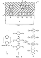
- Dispositif à semi-conducteurs (10) comprenant :un premier conducteur (22) et un deuxième conducteur (24) disposés au voisinage l'un de l'autre ;un corps intermétallique (46) formé à partir d'un matériau diélectrique et disposé entre le premier conducteur métallique et le deuxième conducteur métallique, caractérisé en ce que le matériau diélectrique est un matériau polymérique se composant d'un mélange de poly(para-xylylène) perfluoré et de poly(para-xylylène) non perfluoré.
- Matériau diélectrique intermétallique destiné à des circuits intégrés, se composant:d'un mélange polymérique de poly(para-xylylène) perfluoré et de poly(para-xylylène) non perfluoré.
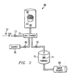
- Procédé de formation d'un matériau diélectrique intermétallique destiné à des circuits intégrés, comprenant les étapes consistant à:- sublimer des dimères de poly(para-xylylène) (60) et les dissocier en des monomères réactifs (62) de poly(para-xylylène);- exposer les monomères réactifs de poly(para-xylylène) à un agent fluorant ; et- déposer le mélange de monomères réactifs (64) de poly(para-xylylène) perfluoré et de poly(para-xylylène) non perfluoré qui en résulte sur un substrat afin de former un matériau diélectrique polymérique se composant d'un mélange de poly(para-xylylène) perfluoré et de poly(para-xylylène) non perfluoré.
- Procédé selon la revendication 3, comprenant en outre le fait d'effectuer l'étape consistant à déposer à une température basse.
- Procédé selon la revendication 3 ou la revendication 4, dans lequel l'étape consistant à exposer comprend l'étape consistant à exposer les monomères en cours de réaction à un agent fluorant comprenant le fluorure de cobalt.
- Procédé selon la revendication 3 ou la revendication 4, dans lequel l'étape consistant à exposer comprend l'étape consistant à exposer les monomères en cours de réaction à un agent fluorant comprenant le fluorure de potassium.
- Procédé selon la revendication 3 ou la revendication 4, dans lequel l'étape consistant à exposer comprend l'étape consistant à exposer les monomères en cours de réaction à un agent fluorant comprenant le fluorure d'hydrogène.
- Appareil destiné à former un matériau diélectrique se composant d'un mélange de poly(para-xylylène) perfluoré et de poly(para-xylylène) non perfluoré sur un substrat (88), comprenant :une source de dimères de poly(para-xylylène) ;une chambre de sublimation (68), agencée de manière à sublimer ladite source de dimères de poly(para-xylylène) ;un four de dissociation (70) couplé à la sortie de la chambre de sublimation, le four de dissociation étant configuré pour dissocier les dimères de poly(para-xylylène) en monomères de poly(para-xylylène) ; etune chambre de condensation (82) couplée à la sortie du four, la chambre de condensation étant configurée pour condenser les monomères de poly(para-xylylène) provenant de la sortie de four sur le substrat ; caractérisé en ce qu'il comprend en outre :une source de fluorure (71, 72) agencée pour la fluoration desdits monomères de poly(para-xylylène) avant la condensation, de telle manière qu'un mélange de poly(para-xylylène) perfluoré et de poly(para-xylylène) non perfluoré est obtenu.
- Appareil selon la revendication 8 :dans lequel la source de fluorure est une source solide de fluorure située dans le four.
- Appareil selon la revendication 9, dans lequel la source solide de fluorure comprend le fluorure de cobalt ou le fluorure de potassium.
- Appareil selon l'une quelconque des revendications 8 à 10, comprenant :un moyen destiné à introduire un agent fluorant gazeux.
- Appareil selon la revendication 11, dans lequel l'agent fluorant gazeux comprend le fluorure d'hydrogène.
- Appareil selon la revendication 11 ou la revendication 12, comprenant en outre :une chambre de mélange destinée à exposer lesdits monomères audit agent fluorant gazeux.
- Appareil selon l'une quelconque des revendications 8 à 13, comprenant en outre :une source destinée à alimenter en dopants ou autres matériaux réactifs ou non réactifs la chambre de mélange.
- Appareil selon l'une quelconque des revendications 8 à 14, dans lequel la température de ladite chambre de condensation est contrôlable entre des températures de l'ordre de -80° à 80°.
- Procédé de formation d'un dispositif à semi-conducteurs comprenant les étapes consistant à :- former sur un substrat un premier (22) et un deuxième (24) éléments conducteurs séparés l'un de l'autre ; et- déposer un matériau diélectrique intermétallique (46) entre le premier et le deuxième éléments conducteurs, se composant d'un mélange de poly(para-xylylène) perfluoré et de poly(para-xylylène) non fluoré.
- Procédé selon la revendication 16, dans lequel l'étape consistant à déposer le diélectrique intermétallique comprend en outre les étapes consistant à :- sublimer une vapeur de monomères de poly(para-xylylène) provenant d'une source de polymères de poly(para-xylylène) ;- chauffer la vapeur de dimères de poly(para-xylylène) afin de dissocier les monomères de poly(para-xylylène) à l'intérieur des dimères de poly(para-xylylène) ;- introduire un agent fluorant vers l'intérieur des monomères de poly(para-xylylène) dissociés ; et- condenser le mélange de l'agent fluorant et les monomères de poly(para-xylylène) dissociés sur la surface entre le premier et le deuxième éléments conducteurs de manière à former ledit matériau de diélectrique intermétallique (46).
- Procédé selon la revendication 17, dans lequel l'étape consistant à introduire un agent fluorant comprend l'étape consistant à introduire une source de fluorure de potassium.
- Procédé selon la revendication 17, dans lequel l'étape consistant à introduire un agent fluorant comprend l'étape consistant à introduire une source de fluorure d'hydrogène.
Applications Claiming Priority (2)
| Application Number | Priority Date | Filing Date | Title |
|---|---|---|---|
| US1389296P | 1996-03-22 | 1996-03-22 | |
| US13892 | 1996-03-22 |
Publications (3)
| Publication Number | Publication Date |
|---|---|
| EP0809291A2 EP0809291A2 (fr) | 1997-11-26 |
| EP0809291A3 EP0809291A3 (fr) | 1998-04-29 |
| EP0809291B1 true EP0809291B1 (fr) | 2007-04-04 |
Family
ID=21762362
Family Applications (1)
| Application Number | Title | Priority Date | Filing Date |
|---|---|---|---|
| EP97103728A Expired - Lifetime EP0809291B1 (fr) | 1996-03-22 | 1997-03-06 | Dispositif semi-conducteur diélectrique entre deux couches de métallisation et procédé de fabrication |
Country Status (5)
| Country | Link |
|---|---|
| EP (1) | EP0809291B1 (fr) |
| JP (1) | JPH1041473A (fr) |
| KR (1) | KR970067387A (fr) |
| DE (1) | DE69737542T2 (fr) |
| TW (1) | TW346660B (fr) |
Families Citing this family (2)
| Publication number | Priority date | Publication date | Assignee | Title |
|---|---|---|---|---|
| JP3199006B2 (ja) * | 1997-11-18 | 2001-08-13 | 日本電気株式会社 | 層間絶縁膜の形成方法および絶縁膜形成装置 |
| JP2000003909A (ja) * | 1998-06-15 | 2000-01-07 | Kishimoto Sangyo Co Ltd | 半導体デバイス用絶縁膜および半導体デバイス |
Citations (2)
| Publication number | Priority date | Publication date | Assignee | Title |
|---|---|---|---|---|
| US3332891A (en) * | 1963-09-23 | 1967-07-25 | Union Carbide Corp | Process for the preparation of alpha-per-fluoro-p-xylylene polymers |
| GB1146005A (en) * | 1965-06-25 | 1969-03-19 | Union Carbide Corp | Gaseous electrical glow discharge etching of para-xylene polymers |
Family Cites Families (4)
| Publication number | Priority date | Publication date | Assignee | Title |
|---|---|---|---|---|
| JPS6437872A (en) * | 1987-08-04 | 1989-02-08 | Seiko Epson Corp | Nonvolatile memory |
| US5656830A (en) * | 1992-12-10 | 1997-08-12 | International Business Machines Corp. | Integrated circuit chip composite having a parylene coating |
| US5373627A (en) * | 1993-11-23 | 1994-12-20 | Grebe; Kurt R. | Method of forming multi-chip module with high density interconnections |
| JPH08139194A (ja) * | 1994-04-28 | 1996-05-31 | Texas Instr Inc <Ti> | 半導体デバイス上に電気接続を作製する方法および該方法により作製された電気接続を有する半導体デバイス |
-
1997
- 1997-03-06 DE DE69737542T patent/DE69737542T2/de not_active Expired - Lifetime
- 1997-03-06 EP EP97103728A patent/EP0809291B1/fr not_active Expired - Lifetime
- 1997-03-21 JP JP9068405A patent/JPH1041473A/ja active Pending
- 1997-03-21 KR KR1019970009781A patent/KR970067387A/ko not_active Application Discontinuation
- 1997-03-28 TW TW086103979A patent/TW346660B/zh not_active IP Right Cessation
Patent Citations (2)
| Publication number | Priority date | Publication date | Assignee | Title |
|---|---|---|---|---|
| US3332891A (en) * | 1963-09-23 | 1967-07-25 | Union Carbide Corp | Process for the preparation of alpha-per-fluoro-p-xylylene polymers |
| GB1146005A (en) * | 1965-06-25 | 1969-03-19 | Union Carbide Corp | Gaseous electrical glow discharge etching of para-xylene polymers |
Also Published As
| Publication number | Publication date |
|---|---|
| EP0809291A3 (fr) | 1998-04-29 |
| EP0809291A2 (fr) | 1997-11-26 |
| TW346660B (en) | 1998-12-01 |
| DE69737542T2 (de) | 2007-12-13 |
| DE69737542D1 (de) | 2007-05-16 |
| KR970067387A (ko) | 1997-10-13 |
| JPH1041473A (ja) | 1998-02-13 |
Similar Documents
| Publication | Publication Date | Title |
|---|---|---|
| US6724086B1 (en) | Hydrogenated oxidized silicon carbon material | |
| US6346747B1 (en) | Method for fabricating a thermally stable diamond-like carbon film as an intralevel or interlevel dielectric in a semiconductor device and device made | |
| US6337518B1 (en) | Low dielectric constant amorphous fluorinated carbon and method of preparation | |
| US5461003A (en) | Multilevel interconnect structure with air gaps formed between metal leads | |
| US7242098B2 (en) | Barrier film integrity on porous low k dielectrics by application of a hydrocarbon plasma treatment | |
| KR100372216B1 (ko) | O.5 및 0.5 미크론 이하의 ulsi 회로용 인터레벨 유전체소자로서의수소실세큐옥산계유동가능한산화물 | |
| US7435685B2 (en) | Method of forming a low-K dual damascene interconnect structure | |
| KR100495896B1 (ko) | 실리콘 카바이드 접착 프로모터 층을 이용하여 저유전상수플루오르화 비결정 탄소에 대한 실리콘 질화물의 접착을강화하는 방법 | |
| US6541398B2 (en) | Ultralow dielectric constant material as an intralevel or interlevel dielectric in a semiconductor device and electronic device containing the same | |
| KR100752940B1 (ko) | 상호접속 구조의 금속간 용량을 감소시키는 공극 금속배선 구성의 제조 방법 | |
| US20020048969A1 (en) | Method of forming film, method of manufacturing semiconductor device, and film forming apparatus | |
| US5828132A (en) | Semiconductor device having perfluorinated and non-fluorinated parylene intermetal dielectric | |
| US6790789B2 (en) | Ultralow dielectric constant material as an intralevel or interlevel dielectric in a semiconductor device and electronic device made | |
| US6953984B2 (en) | Hydrogenated oxidized silicon carbon material | |
| US7056839B2 (en) | Method of forming a silica insulation film with a reduced dielectric constant | |
| EP0809291B1 (fr) | Dispositif semi-conducteur diélectrique entre deux couches de métallisation et procédé de fabrication | |
| JP2004200203A (ja) | 半導体装置及びその製造方法 | |
| US20040119163A1 (en) | Method of making semiconductor devices using carbon nitride, a low-dielectric-constant hard mask and/or etch stop | |
| US20030209805A1 (en) | Flourine doped SiO2 film and method of fabrication | |
| Treichel et al. | New dielectric materials and insulators for microelectronic applications | |
| WO2002021593A9 (fr) | Procede de production de films au nitrure de titane (tin) par depot chimique en phase vapeur de substances organo-metalliques | |
| Ruhl et al. | Deposition of titanium nitride/tungsten layers for application in vertically integrated circuits technology | |
| Jeng et al. | Process integration of low-dielectric-constant materials | |
| US6632737B1 (en) | Method for enhancing the adhesion of a barrier layer to a dielectric | |
| Park et al. | High-quality conformal silicon oxide films prepared by multi-step sputtering PECVD and chemical mechanical polishing |
Legal Events
| Date | Code | Title | Description |
|---|---|---|---|
| PUAI | Public reference made under article 153(3) epc to a published international application that has entered the european phase |
Free format text: ORIGINAL CODE: 0009012 |
|
| AK | Designated contracting states |
Kind code of ref document: A2 Designated state(s): DE FR GB IT NL |
|
| PUAL | Search report despatched |
Free format text: ORIGINAL CODE: 0009013 |
|
| AK | Designated contracting states |
Kind code of ref document: A3 Designated state(s): DE FR GB IT NL |
|
| 17P | Request for examination filed |
Effective date: 19981029 |
|
| 17Q | First examination report despatched |
Effective date: 20010612 |
|
| GRAP | Despatch of communication of intention to grant a patent |
Free format text: ORIGINAL CODE: EPIDOSNIGR1 |
|
| GRAS | Grant fee paid |
Free format text: ORIGINAL CODE: EPIDOSNIGR3 |
|
| GRAA | (expected) grant |
Free format text: ORIGINAL CODE: 0009210 |
|
| AK | Designated contracting states |
Kind code of ref document: B1 Designated state(s): DE FR GB IT NL |
|
| REG | Reference to a national code |
Ref country code: GB Ref legal event code: FG4D |
|
| REF | Corresponds to: |
Ref document number: 69737542 Country of ref document: DE Date of ref document: 20070516 Kind code of ref document: P |
|
| ET | Fr: translation filed | ||
| NLV1 | Nl: lapsed or annulled due to failure to fulfill the requirements of art. 29p and 29m of the patents act | ||
| PG25 | Lapsed in a contracting state [announced via postgrant information from national office to epo] |
Ref country code: NL Free format text: LAPSE BECAUSE OF FAILURE TO SUBMIT A TRANSLATION OF THE DESCRIPTION OR TO PAY THE FEE WITHIN THE PRESCRIBED TIME-LIMIT Effective date: 20070404 |
|
| PLBE | No opposition filed within time limit |
Free format text: ORIGINAL CODE: 0009261 |
|
| STAA | Information on the status of an ep patent application or granted ep patent |
Free format text: STATUS: NO OPPOSITION FILED WITHIN TIME LIMIT |
|
| 26N | No opposition filed |
Effective date: 20080107 |
|
| PG25 | Lapsed in a contracting state [announced via postgrant information from national office to epo] |
Ref country code: IT Free format text: LAPSE BECAUSE OF FAILURE TO SUBMIT A TRANSLATION OF THE DESCRIPTION OR TO PAY THE FEE WITHIN THE PRESCRIBED TIME-LIMIT Effective date: 20070404 |
|
| PGFP | Annual fee paid to national office [announced via postgrant information from national office to epo] |
Ref country code: FR Payment date: 20120328 Year of fee payment: 16 |
|
| PGFP | Annual fee paid to national office [announced via postgrant information from national office to epo] |
Ref country code: GB Payment date: 20120227 Year of fee payment: 16 |
|
| PGFP | Annual fee paid to national office [announced via postgrant information from national office to epo] |
Ref country code: DE Payment date: 20120330 Year of fee payment: 16 |
|
| GBPC | Gb: european patent ceased through non-payment of renewal fee |
Effective date: 20130306 |
|
| REG | Reference to a national code |
Ref country code: FR Ref legal event code: ST Effective date: 20131129 |
|
| REG | Reference to a national code |
Ref country code: DE Ref legal event code: R119 Ref document number: 69737542 Country of ref document: DE Effective date: 20131001 |
|
| PG25 | Lapsed in a contracting state [announced via postgrant information from national office to epo] |
Ref country code: GB Free format text: LAPSE BECAUSE OF NON-PAYMENT OF DUE FEES Effective date: 20130306 Ref country code: FR Free format text: LAPSE BECAUSE OF NON-PAYMENT OF DUE FEES Effective date: 20130402 Ref country code: DE Free format text: LAPSE BECAUSE OF NON-PAYMENT OF DUE FEES Effective date: 20131001 |