EP0809291B1 - Halbleiterschaltung mit dielektrischer Schicht zwischen zwei Metallebenen und Verfahren zur Herstellung - Google Patents
Halbleiterschaltung mit dielektrischer Schicht zwischen zwei Metallebenen und Verfahren zur Herstellung Download PDFInfo
- Publication number
- EP0809291B1 EP0809291B1 EP97103728A EP97103728A EP0809291B1 EP 0809291 B1 EP0809291 B1 EP 0809291B1 EP 97103728 A EP97103728 A EP 97103728A EP 97103728 A EP97103728 A EP 97103728A EP 0809291 B1 EP0809291 B1 EP 0809291B1
- Authority
- EP
- European Patent Office
- Prior art keywords
- xylylene
- para
- poly
- monomers
- perfluorinated
- Prior art date
- Legal status (The legal status is an assumption and is not a legal conclusion. Google has not performed a legal analysis and makes no representation as to the accuracy of the status listed.)
- Expired - Lifetime
Links
Images
Classifications
-
- H10W20/071—
-
- H10W20/48—
-
- H10W20/495—
Definitions
- This invention relates in general to the field of electronic devices and more particularly to semiconductor devices having an improved intermetal dielectric and method of formation.
- the interconnect RC time constant increases rapidly because the resistance of metal leads increases with decreasing line width and the interconnect capacitance increases with decreasing spacing between the lines.
- the interconnect delay becomes a major limiting factor of circuit performance.
- dielectric materials there are a variety of dielectric materials including pure polymer, spin-on glasses, and porous materials that offer lower values of permittivity than traditional silicon dioxide.
- One particularly useful polymer which exhibits extremely low permittivity values and yet exhibits thermal stability is fluorinated poly (para-xylylene), commonly referred to as fluorinated parylene or parylene-F.
- Parylene-F exhibits a dielectric constant on the order of 2.3. This is in comparison to a dielectric constant of on the order of 2.7 for non-fluorinated parylene, commonly referred to as parylene-N, and a dielectric constant of the order of 4.5 for undoped silicon dioxide.
- parylene-F performs as an excellent intermetal dielectric, it is extremely difficult to work with because of the difficulty in forming the precursor dimer AF4 which is the reactant needed to the formation of parylene-F. Methods of forming the necessary precursor dimer are extremely difficult to control and have correspondingly low yield rates. As such, the precursor dimer for parylene-F is not commercially available and the use of parylene-F as an intermetal dielectric is not commercially feasible.
- an intermetal dielectric material is provided that substantially eliminates or reduces problems associated with prior materials and techniques of formation.
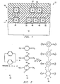
- a semiconductor structure indicated generally at 10 is shown which is formed on the outer surface of a semiconductor substrate 12 which may comprise any suitable semiconductor material such as silicon or gallium arsenide.
- Semiconductor structure 10 comprises a first level of conductive interconnects indicated generally at 14 and a second level of conductive interconnects indicated generally at 16.
- Level 14 and level 16 are interconnected by conductive vias represented by via 18 shown in FIGURE 1.
- Level 14 comprises a network of conductive elements represented by conductive elements 20, 22, 24 and 26.
- Each of the conductive elements 20, 22, 24 and 26 comprise a composite structure of metal and nitride.
- conductive element 20 comprises a first level of titanium nitride 28.
- a layer of aluminum 30 is disposed outwardly from layer 28.
- an outer layer of titanium nitride 32 is disposed outwardly from layer 30.
- Each of conductive elements 20, 22, 24 and 26 are constructed of such a composite formation.
- layer 16 is comprised of a network of conductors represented by conductive elements 34, 36', and 38. Level 16 may be connected to other outer layers of conductors or devices by conductive via 40. Conductive elements 34, 36 and 38 are each comprised of composite structures similar to that described with reference to element 20 previously.
- Level 14 is separated from level 16 and some elements within level 14 are separated from one another by a silicon dioxide layer 42. Similarly, level 16 is separated from layers formed outwardly from level 16 and certain of the elements within layer 16 or separated from one another by a second silicon dioxide layer 44.
- conductive elements which are spaced apart by the minimum geometric spacing are not separated by silicon dioxide.
- conductive elements 22 and 24 are spaced apart by an elongate polymer body 46 shown in FIGURE 1.
- conductive elements 24 and 26 are spaced apart by an elongate polymer body 48.
- conductive elements 36 and 38 are spaced apart by an elongate polymer body 50.
- Polymer bodies 46, 48 and 50 comprise the intermetal dielectric materials, the formation of which will be described herein.
- bodies 46, 48 and 50 are formed of a mixture of perfluorinated and non-fluorinated parylene which exhibits a dielectric constant of the order of 2.3.
- This dielectric constant and the overall performance of the mixed polymeric material is comparable to a fluorinated parylene, commonly referred to as parylene-F.
- the mixed polymer material is much easier to form and, as such, is a commercially feasible intermetal dielectric.
- the polymer bodies 46, 48 and 50 and formed by a conformal deposition of the mixed polymeric material. This deposition process is followed by an etch-back process. These processes may result in the residual sidewall bodies shown in FIGURE 1 and exemplified by residual sidewall bodies 50 and 52 disposed outwardly from conductive elements 22 and 26 respectively.
- FIGURE 2 is a diagram which illustrates the chemical processes that are used to form the mixed polymeric material used in the present invention.
- a conventional parylene-N, parylene-C or parylene-D dimer indicated at 60 is decomposed to create the reactive monomers indicated generally at 62.
- These reactive monomers are subjected to an environment which includes fluoride-carrying agents.
- fluoride-carrying agents may comprise, for example, cobalt fluoride (CoF 3 ), potassium fluoride (KF), or hydrogen fluoride (HF).
- CoF 3 cobalt fluoride
- KF potassium fluoride
- HF hydrogen fluoride
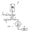
- System 66 is under vacuum base pressure of less than 10 millitor.
- System 66 comprises a dimer source 68 which is connected to a furnace 70.
- Furnace 70 also comprises a solid fluoride source 71, which introduces into furnace 70 a solid source of fluoride which may comprise, for example, cobalt fluoride or potassium fluoride.
- a gaseous fluoridating agent such as hydrogen fluoride may introduced from an HF source 72 through a valve 73 to a mix chamber 74.
- the dimer source 68 supplies the parylene-N, parylene-C or parylene-D dimer vapor by subliming the dimer by heating the dimer to on the order of 120° - 150°C.
- Furnace 70 is heated to the order of 500-580°C to disassociate the dimers and create the mixture of monomers and reactive fluoride compounds.
- This mixture is then passed to mixing chamber 74 through a valve 76.
- Other materials, such as dopants or other reactive or non-reactive agents may be supplied to the mix chamber 74 from a source 78 through a valve 80.
- a gaseous fluoride source such as HF source 72 is used, the mixing chamber 74 is used to fluoridate the reactive monomers.
- the mixing chamber 74 is connected to a chamber 82.
- the entire system 66 is kept at a base pressure of less than 10 millitor.
- the pressure within chamber 82 increases during the deposition process but does not exceed 100 millitor. This pressure can be controlled by the temperature of dimer source 68 or by controlling the mass flow of the vapor entering the chamber 82.
- a chuck 83 within chamber 82 is capable of being temperature controlled between -80°C and 80°C.
- the chuck 83 inside the chamber 82 is cooled or heated to between -40° and 10°C to enable the monomers and fluoride to condense on the surface of a semiconductor wafer 88 placed on the chuck 83 within chamber 82.
- the dimer source 68 provides an environment where the solid dimer can sublimate to a vapor state before being passed into furnace 70.
- the furnace 70 then disassociates the vapor dimer to the required reactive monomers.
- the fluoride source 72 then introduces the fluorinating agent into the furnace 70.
- the resulting reactive mixture is then condensed to form a mixture of per-fluorinated and non-fluorinated parylene on the outer surface of wafer 88 within CVD chamber 82.
- This mixed polymeric material exhibits a dielectric constant of the order of 2.3. It is thus comparable to the expensive and impractical parylene-F material.
- the mixed polymer intermetal dielectric of the present invention maintains good dimensional stability, high thermal stability, ease of pattern and etch for sub-micron features, low moisture absorption and permeation, good adhesion, low stress, good etch selectivity to metal, high thermal conductivity, high dielectric strength/low leakage current and good gap filling and planarization capability.
Landscapes
- Internal Circuitry In Semiconductor Integrated Circuit Devices (AREA)
- Formation Of Insulating Films (AREA)
- Compositions Of Macromolecular Compounds (AREA)
- Semiconductor Integrated Circuits (AREA)
- Organic Insulating Materials (AREA)
Claims (19)
- Halbleiterbauelement (10) mit:einem ersten Leiter (22) und einem zweiten Leiter (24), die angrenzend zueinander angeordnet sind,einem Intermetallkörper (46), der aus einem dielektrischen Material besteht und zwischen dem ersten Metallleiter und dem zweiten Metallleiter angeordnet ist,dadurch gekennzeichnet, dass
das dielektrische Material ein Polymermaterial ist, das aus einer Mischung von perfluoriertem Poly(para-xylylen) und nicht perfluoriertem Poly(para-xylylen) besteht. - Dielektrisches Intermetallmaterial für integrierte Schaltungen, das aus einer Polymermischung von perfluoriertem Poly(para-xylylen) und nicht perfluoriertem Poly(para-xylylen) besteht.
- Verfahren zum Bilden eines dielektrischen Intermetallmaterials für integrierte Schaltungen mit den folgenden Schritten:Sublimieren von Poly(para-xylylen)dimeren (60) und Dissoziieren von ihnen zu reaktiven Poly(para-xylylen)monomeren (62),Einwirkenlassen eines Fluorierungsmittels auf die reaktiven Poly(para-xylylen)monomere undAbscheiden der sich ergebenden Mischung perfluorierter und nicht perfluorierter reaktiver Poly(para-xylylen)monomere (64) auf ein Substrat zur Bildung eines dielektrischen Polymermaterials, welches aus einer Mischung von perfluoriertem Poly(para-xylylen) und nicht perfluoriertem Poly(para-xylylen) besteht.
- Verfahren nach Anspruch 3, bei dem weiter der Abscheidungsschritt bei einer niedrigen Temperatur ausgeführt wird.
- Verfahren nach Anspruch 3 oder 4, wobei in dem Schritt des Einwirkenlassens die reaktiven Monomere einem Fluorierungsmittel ausgesetzt werden, das Kobaltfluorid enthält.
- Verfahren nach Anspruch 3 oder 4, wobei in dem Schritt des Einwirkenlassens die reaktiven Monomere einem Fluorierungsmittel ausgesetzt werden, welches Kaliumfluorid enthält.
- Verfahren nach Anspruch 3 oder 4, wobei in dem Schritt des Einwirkenlassens die reaktiven Monomere einem Fluorierungsmittel ausgesetzt werden, das Fluorwasserstoff enthält.
- Vorrichtung zum Bilden eines dielektrischen Materials, das aus einer Mischung von perfluoriertem Poly(para-xylylen) und nicht perfluoriertem Poly(para-xylylen) besteht, auf einem Substrat (88) mit:einer Poly(para-xylylen)dimerquelle,einer Sublimationskammer (68), die für das Sublimieren der Poly(para-xylylen)dimerquelle eingerichtet ist,einem Dissoziationsofen (70), der mit dem Ausgang der Sublimationskammer verbunden ist, wobei der Dissoziationsofen für das Dissoziieren der Poly(para-xylylen)dimere zu Poly(para-xylylen)monomeren konfiguriert ist, undeiner Kondensationskammer (82), die mit dem Ausgang des Ofens verbunden ist, wobei die Kondensationskammer konfiguriert ist, um die Poly(para-xylylen)monomere von dem Ausgang des Ofens auf dem Substrat zu kondensieren,dadurch gekennzeichnet, dass sie weiter aufweist:eine Fluoridquelle (71, 72), die für das Fluorieren der Poly(para-xylylen)monomere vor dem Kondensieren eingerichtet ist, so dass eine Mischung von perfluoriertem Poly(para-xylylen) und nicht perfluoriertem Poly(para-xylylen) erhalten wird.
- Vorrichtung nach Anspruch 8, wobei die Fluoridquelle eine feste Fluoridquelle ist, die sich in dem Ofen befindet.
- Vorrichtung nach Anspruch 9, wobei die feste Fluoridquelle Kobaltfluorid oder Kaliumfluorid enthält.
- Vorrichtung nach einem der Ansprüche 8 bis 10 mit:Mitteln zum Einleiten eines gasförmigen Fluoridierungsmittels.
- Vorrichtung nach Anspruch 11, wobei das gasförmige Fluoridierungsmittel Fluorwasserstoff enthält.
- Vorrichtung nach Anspruch 11 oder 12, welche weiter aufweist:eine Mischkammer, um das gasförmige Fluoridierungsmittel auf die Monomere einwirken zu lassen.
- Vorrichtung nach einem der Ansprüche 8 bis 13, welche weiter aufweist:eine Quelle zum Zuführen von Dotierungsmaterialien oder anderen reaktiven oder nicht reaktiven Materialien zu der Mischkammer.
- Vorrichtung nach einem der Ansprüche 8 bis 14, wobei die Temperatur der Kondensationskammer zwischen Temperaturen in der Größenordnung von -80 °C und 80 °C steuerbar ist.
- Verfahren zum Bilden eines Halbleiterbauelements mit den folgenden Schritten:Bilden erster (22) und zweiter (24) leitfähiger Elemente, die voneinander beabstandet sind, auf einem Substrat undAbscheiden eines dielektrischen Intermetallmaterials (46) zwischen den ersten und zweiten leitfähigen Elementen, das aus einer Mischung von perfluoriertem Poly(para-xylylen) und nicht perfluoriertem Poly(para-xylylen) besteht.
- Verfahren nach Anspruch 16, wobei der Schritt des Abscheidens des Intermetalldielektrikums weiter aufweist:Sublimieren eines Poly(para-xylylen)dimerdampfs von einer Poly(para-xylylen)dimerquelle,Erwärmen des Poly(para-xylylen)dimerdampfs, um die Poly(para-xylylen)monomere innerhalb des Poly(para-xylylen)dimers zu dissoziieren,Einleiten eines Fluoridierungsmittels in die dissoziierten Poly(para-xylylen)monomere undKondensieren der Mischung des Fluoridierungsmittels und der dissoziierten Poly(para-xylylen)monomere an der Oberfläche zwischen den ersten und zweiten leitfähigen Elementen, um das dielektrische Intermetallmaterial (46) zu bilden.
- Verfahren nach Anspruch 17, wobei in dem Schritt des Einleitens eines Fluoridierungsmittels eine Kaliumfluoridquelle eingeleitet wird.
- Verfahren nach Anspruch 17, wobei in dem Schritt des Einleitens eines Fluoridierungsmittels eine Fluoridwasserstoffquelle eingeleitet wird.
Applications Claiming Priority (2)
| Application Number | Priority Date | Filing Date | Title |
|---|---|---|---|
| US1389296P | 1996-03-22 | 1996-03-22 | |
| US13892 | 1996-03-22 |
Publications (3)
| Publication Number | Publication Date |
|---|---|
| EP0809291A2 EP0809291A2 (de) | 1997-11-26 |
| EP0809291A3 EP0809291A3 (de) | 1998-04-29 |
| EP0809291B1 true EP0809291B1 (de) | 2007-04-04 |
Family
ID=21762362
Family Applications (1)
| Application Number | Title | Priority Date | Filing Date |
|---|---|---|---|
| EP97103728A Expired - Lifetime EP0809291B1 (de) | 1996-03-22 | 1997-03-06 | Halbleiterschaltung mit dielektrischer Schicht zwischen zwei Metallebenen und Verfahren zur Herstellung |
Country Status (5)
| Country | Link |
|---|---|
| EP (1) | EP0809291B1 (de) |
| JP (1) | JPH1041473A (de) |
| KR (1) | KR970067387A (de) |
| DE (1) | DE69737542T2 (de) |
| TW (1) | TW346660B (de) |
Families Citing this family (2)
| Publication number | Priority date | Publication date | Assignee | Title |
|---|---|---|---|---|
| JP3199006B2 (ja) * | 1997-11-18 | 2001-08-13 | 日本電気株式会社 | 層間絶縁膜の形成方法および絶縁膜形成装置 |
| JP2000003909A (ja) * | 1998-06-15 | 2000-01-07 | Kishimoto Sangyo Co Ltd | 半導体デバイス用絶縁膜および半導体デバイス |
Citations (2)
| Publication number | Priority date | Publication date | Assignee | Title |
|---|---|---|---|---|
| US3332891A (en) * | 1963-09-23 | 1967-07-25 | Union Carbide Corp | Process for the preparation of alpha-per-fluoro-p-xylylene polymers |
| GB1146005A (en) * | 1965-06-25 | 1969-03-19 | Union Carbide Corp | Gaseous electrical glow discharge etching of para-xylene polymers |
Family Cites Families (4)
| Publication number | Priority date | Publication date | Assignee | Title |
|---|---|---|---|---|
| JPS6437872A (en) * | 1987-08-04 | 1989-02-08 | Seiko Epson Corp | Nonvolatile memory |
| US5656830A (en) * | 1992-12-10 | 1997-08-12 | International Business Machines Corp. | Integrated circuit chip composite having a parylene coating |
| US5373627A (en) * | 1993-11-23 | 1994-12-20 | Grebe; Kurt R. | Method of forming multi-chip module with high density interconnections |
| JPH08139194A (ja) * | 1994-04-28 | 1996-05-31 | Texas Instr Inc <Ti> | 半導体デバイス上に電気接続を作製する方法および該方法により作製された電気接続を有する半導体デバイス |
-
1997
- 1997-03-06 EP EP97103728A patent/EP0809291B1/de not_active Expired - Lifetime
- 1997-03-06 DE DE69737542T patent/DE69737542T2/de not_active Expired - Lifetime
- 1997-03-21 KR KR1019970009781A patent/KR970067387A/ko not_active Ceased
- 1997-03-21 JP JP9068405A patent/JPH1041473A/ja active Pending
- 1997-03-28 TW TW086103979A patent/TW346660B/zh not_active IP Right Cessation
Patent Citations (2)
| Publication number | Priority date | Publication date | Assignee | Title |
|---|---|---|---|---|
| US3332891A (en) * | 1963-09-23 | 1967-07-25 | Union Carbide Corp | Process for the preparation of alpha-per-fluoro-p-xylylene polymers |
| GB1146005A (en) * | 1965-06-25 | 1969-03-19 | Union Carbide Corp | Gaseous electrical glow discharge etching of para-xylene polymers |
Also Published As
| Publication number | Publication date |
|---|---|
| KR970067387A (ko) | 1997-10-13 |
| TW346660B (en) | 1998-12-01 |
| DE69737542D1 (de) | 2007-05-16 |
| EP0809291A3 (de) | 1998-04-29 |
| EP0809291A2 (de) | 1997-11-26 |
| DE69737542T2 (de) | 2007-12-13 |
| JPH1041473A (ja) | 1998-02-13 |
Similar Documents
| Publication | Publication Date | Title |
|---|---|---|
| US6724086B1 (en) | Hydrogenated oxidized silicon carbon material | |
| US6346747B1 (en) | Method for fabricating a thermally stable diamond-like carbon film as an intralevel or interlevel dielectric in a semiconductor device and device made | |
| US6337518B1 (en) | Low dielectric constant amorphous fluorinated carbon and method of preparation | |
| US7242098B2 (en) | Barrier film integrity on porous low k dielectrics by application of a hydrocarbon plasma treatment | |
| KR100372216B1 (ko) | O.5 및 0.5 미크론 이하의 ulsi 회로용 인터레벨 유전체소자로서의수소실세큐옥산계유동가능한산화물 | |
| US7435685B2 (en) | Method of forming a low-K dual damascene interconnect structure | |
| US6479110B2 (en) | Multiphase low dielectric constant material and method of deposition | |
| KR100495896B1 (ko) | 실리콘 카바이드 접착 프로모터 층을 이용하여 저유전상수플루오르화 비결정 탄소에 대한 실리콘 질화물의 접착을강화하는 방법 | |
| KR100378614B1 (ko) | 금속리드사이에형성된에어갭을갖고있는다중레벨상호연결구조물 | |
| EP1209739A2 (de) | Verfahren zur Hestellung von Zwischenmetall-Dielektrikanwendungen mit Luftspalten zwischen Metall-Leitern | |
| US20020180051A1 (en) | Ultralow dielectric constant material as an intralevel or interlevel dielectric in a semiconductor device and electronic device containing the same | |
| US20020048969A1 (en) | Method of forming film, method of manufacturing semiconductor device, and film forming apparatus | |
| US6858526B2 (en) | Methods of forming materials between conductive electrical components, and insulating materials | |
| US5828132A (en) | Semiconductor device having perfluorinated and non-fluorinated parylene intermetal dielectric | |
| US6953984B2 (en) | Hydrogenated oxidized silicon carbon material | |
| US20030143865A1 (en) | Ultralow dielectric constant material as an intralevel or interlevel dielectric in a semiconductor device and electronic device made | |
| EP0726599B1 (de) | Verfahren zum Herstellen einer Halbleiteranordnung mit einer Mehrschichtverbindungsstruktur, mit einem verbesserten Schritt zum Herstellen einer dielektrischen Zwischenschicht | |
| US7056839B2 (en) | Method of forming a silica insulation film with a reduced dielectric constant | |
| EP0809291B1 (de) | Halbleiterschaltung mit dielektrischer Schicht zwischen zwei Metallebenen und Verfahren zur Herstellung | |
| JP2004200203A (ja) | 半導体装置及びその製造方法 | |
| US20040119163A1 (en) | Method of making semiconductor devices using carbon nitride, a low-dielectric-constant hard mask and/or etch stop | |
| WO2001041203A1 (en) | Improved flourine doped sio2 film | |
| WO2002021593A9 (en) | Method of forming titanium nitride (tin) films using metal-organic chemical vapor deposition (mocvd) | |
| Treichel et al. | New dielectric materials and insulators for microelectronic applications | |
| Ruhl et al. | Deposition of titanium nitride/tungsten layers for application in vertically integrated circuits technology |
Legal Events
| Date | Code | Title | Description |
|---|---|---|---|
| PUAI | Public reference made under article 153(3) epc to a published international application that has entered the european phase |
Free format text: ORIGINAL CODE: 0009012 |
|
| AK | Designated contracting states |
Kind code of ref document: A2 Designated state(s): DE FR GB IT NL |
|
| PUAL | Search report despatched |
Free format text: ORIGINAL CODE: 0009013 |
|
| AK | Designated contracting states |
Kind code of ref document: A3 Designated state(s): DE FR GB IT NL |
|
| 17P | Request for examination filed |
Effective date: 19981029 |
|
| 17Q | First examination report despatched |
Effective date: 20010612 |
|
| GRAP | Despatch of communication of intention to grant a patent |
Free format text: ORIGINAL CODE: EPIDOSNIGR1 |
|
| GRAS | Grant fee paid |
Free format text: ORIGINAL CODE: EPIDOSNIGR3 |
|
| GRAA | (expected) grant |
Free format text: ORIGINAL CODE: 0009210 |
|
| AK | Designated contracting states |
Kind code of ref document: B1 Designated state(s): DE FR GB IT NL |
|
| REG | Reference to a national code |
Ref country code: GB Ref legal event code: FG4D |
|
| REF | Corresponds to: |
Ref document number: 69737542 Country of ref document: DE Date of ref document: 20070516 Kind code of ref document: P |
|
| ET | Fr: translation filed | ||
| NLV1 | Nl: lapsed or annulled due to failure to fulfill the requirements of art. 29p and 29m of the patents act | ||
| PG25 | Lapsed in a contracting state [announced via postgrant information from national office to epo] |
Ref country code: NL Free format text: LAPSE BECAUSE OF FAILURE TO SUBMIT A TRANSLATION OF THE DESCRIPTION OR TO PAY THE FEE WITHIN THE PRESCRIBED TIME-LIMIT Effective date: 20070404 |
|
| PLBE | No opposition filed within time limit |
Free format text: ORIGINAL CODE: 0009261 |
|
| STAA | Information on the status of an ep patent application or granted ep patent |
Free format text: STATUS: NO OPPOSITION FILED WITHIN TIME LIMIT |
|
| 26N | No opposition filed |
Effective date: 20080107 |
|
| PG25 | Lapsed in a contracting state [announced via postgrant information from national office to epo] |
Ref country code: IT Free format text: LAPSE BECAUSE OF FAILURE TO SUBMIT A TRANSLATION OF THE DESCRIPTION OR TO PAY THE FEE WITHIN THE PRESCRIBED TIME-LIMIT Effective date: 20070404 |
|
| PGFP | Annual fee paid to national office [announced via postgrant information from national office to epo] |
Ref country code: FR Payment date: 20120328 Year of fee payment: 16 |
|
| PGFP | Annual fee paid to national office [announced via postgrant information from national office to epo] |
Ref country code: GB Payment date: 20120227 Year of fee payment: 16 |
|
| PGFP | Annual fee paid to national office [announced via postgrant information from national office to epo] |
Ref country code: DE Payment date: 20120330 Year of fee payment: 16 |
|
| GBPC | Gb: european patent ceased through non-payment of renewal fee |
Effective date: 20130306 |
|
| REG | Reference to a national code |
Ref country code: FR Ref legal event code: ST Effective date: 20131129 |
|
| REG | Reference to a national code |
Ref country code: DE Ref legal event code: R119 Ref document number: 69737542 Country of ref document: DE Effective date: 20131001 |
|
| PG25 | Lapsed in a contracting state [announced via postgrant information from national office to epo] |
Ref country code: GB Free format text: LAPSE BECAUSE OF NON-PAYMENT OF DUE FEES Effective date: 20130306 Ref country code: FR Free format text: LAPSE BECAUSE OF NON-PAYMENT OF DUE FEES Effective date: 20130402 Ref country code: DE Free format text: LAPSE BECAUSE OF NON-PAYMENT OF DUE FEES Effective date: 20131001 |