EP0809255B1 - Schieberegisterzelle - Google Patents
Schieberegisterzelle Download PDFInfo
- Publication number
- EP0809255B1 EP0809255B1 EP97111252A EP97111252A EP0809255B1 EP 0809255 B1 EP0809255 B1 EP 0809255B1 EP 97111252 A EP97111252 A EP 97111252A EP 97111252 A EP97111252 A EP 97111252A EP 0809255 B1 EP0809255 B1 EP 0809255B1
- Authority
- EP
- European Patent Office
- Prior art keywords
- input
- output
- signal
- multiplexer
- parallel
- Prior art date
- Legal status (The legal status is an assumption and is not a legal conclusion. Google has not performed a legal analysis and makes no representation as to the accuracy of the status listed.)
- Expired - Lifetime
Links
Images


Classifications
-
- G—PHYSICS
- G01—MEASURING; TESTING
- G01R—MEASURING ELECTRIC VARIABLES; MEASURING MAGNETIC VARIABLES
- G01R31/00—Arrangements for testing electric properties; Arrangements for locating electric faults; Arrangements for electrical testing characterised by what is being tested not provided for elsewhere
- G01R31/28—Testing of electronic circuits, e.g. by signal tracer
- G01R31/317—Testing of digital circuits
- G01R31/3181—Functional testing
- G01R31/3185—Reconfiguring for testing, e.g. LSSD, partitioning
- G01R31/318533—Reconfiguring for testing, e.g. LSSD, partitioning using scanning techniques, e.g. LSSD, Boundary Scan, JTAG
- G01R31/318541—Scan latches or cell details
-
- G—PHYSICS
- G11—INFORMATION STORAGE
- G11C—STATIC STORES
- G11C19/00—Digital stores in which the information is moved stepwise, e.g. shift registers
- G11C19/38—Digital stores in which the information is moved stepwise, e.g. shift registers two-dimensional [2D], e.g. horizontal and vertical shift registers
Definitions
- the present invention relates to a cell for shift register. She finds an interest while particularly in the implementation of operation of specialized integrated circuits.
- ASICs Application Specific Integrated Circuit
- DSP signal processor
- the user provides the manufacturer with the program application and information on the desired circuit configuration such as type and the volume of memories or the nature of the devices circuit interface.
- the integrated circuit is then realized on a chip by associating with the central processing unit specified devices, including read only memory (ROM) containing the application program.
- ROM read only memory
- test program stored in the program memory of the circuit.
- configurations depend on demand of the user, it is not possible to provide a unique test program.
- a disadvantage of this system is that it does not allow direct access to the internal buses of the circuit used for communications between the central unit and application dependent devices, unless dramatically increase the number of cells, this which affects the compactness of the circuit, and the speed of the shift register.
- a cell used to take place in a shift register is connected in series on a line (an access line to a central unit by example) and in series with other cells connected to other lines. Physically, the said line will therefore separated into two parts. For example, if such cell is mounted on a bus line between a unit central and a peripheral, part of the line will go from the central unit to the cell, and the other part of the line will go from cell to device.
- Such a cell therefore includes an input, called parallel, connected to part of the line, an output, called parallel, connected to the other part of the line (for inject a value on this part of the line transmitted from outside via the other cells or for provide the value present on the parallel input to which the cell is transparent), a serial input, and a serial output to allow offset gradually, in the shift register in which this cell takes place, the values to inject or the sampled values.
- the cells can be unidirectional if they are mounted on lines having a defined sense of signal propagation, or bidirectional if mounted on lines used to transmit signals in both directions, in which case the parallel inputs and outputs are actually input / output.
- unidirectional cells typically have a memory flip-flop (for example a master-slave delay scale) capable of receiving as input the value of the signal present on the input parallel (in the case of sampling), either on serial input (in the case of injection or offset), and whose output is connected to the output serial (to allow shifting from one cell to the other).
- a memory flip-flop for example a master-slave delay scale
- they also include conventionally a multiplexer having a connected input at the parallel input, and an input connected to the output of the storage flip-flop, possibly by the through a latch, and an outlet connected to the parallel output, this multiplexer allowing to inject a value on the line, or make the cell transparent to the line (the input and parallel outputs then being connected).
- These different means are controlled by control signals either from an external control block or from a internal control block receiving control signals external, the test procedures of course being controlled from outside the circuit.
- the cell composition is identical, except that they include an additional multiplexer having an input connected to the parallel output (which has an input / output), an input connected to the exit from the storage flip-flop (possibly by through a latch toggle), and an exit connected to the parallel input (which behaves in enter exit).
- an additional multiplexer having an input connected to the parallel output (which has an input / output), an input connected to the exit from the storage flip-flop (possibly by through a latch toggle), and an exit connected to the parallel input (which behaves in enter exit).
- it is necessary to provide an order and an additional entry on the multiplexing means necessary to be able to provide the input of the storage flip-flop ie the value of signal present at the serial input (in case of offset) either the value of one of the signals present on the inputs and parallel outputs (in case of sampling).
- An object of the invention is to propose a cell who has memory capacities, so that he can sample the value of the signal present on the line without stopping the operation of the circuit, and without force to synchronize external offset clocks with the circuit's internal clocks.
- the cell will include a latch with an input receiving the parallel input signal.
- Another object of the invention is to propose a cell which will guarantee the state of the signals present at the input and output of the scales of the cell, and subsequently minimize the consumption of this cell.
- the subject of the invention is the integrated circuit of claim 1.
- the entry of the scale at lock will be connected to the output of a multiplexer, this multiplexer having a connected input at the parallel input and an input connected to the output of the latch toggle.
- Another object of the invention is to propose unidirectional or bidirectional type cells integrating memory and maintenance capabilities toggle input status as defined above.
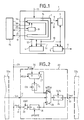
- an integrated circuit 1 made on a silicon chip for example, has a central unit 2 and a number of devices 3, 4, 5 depending on the application of the integrated circuit.
- the devices associated with the central unit 2 include for example a read-only program memory 3 (ROM), a random access data memory 4 (RAM) and one or more schematic interface devices by unit 5. These interface devices are connected to primary accesses 6 of circuit 1 allowing to exchange analog or digital signals with circuit environment 1.
- the central unit is connected to the memory of programs 3 in a classic way, by a bus instructions 8, an instruction address bus 9 and lines of a command output bus 10 allowing read program instructions in memory 3 for execution.
- CPU 2 is connected to devices 4, 5 by a data bus bidirectional 11, a data address bus 12 and lines of the command output bus 10, allowing the central unit 2 to exchange data (transmission or reception) with devices 4, 5.
- the central unit 2 may also include a command input bus 13 for receiving control signals exteriors.
- the unit control unit 2 is provided with a shift register 14.
- This shift register 14, of the "boundary scan" type includes a set of cells elementaries connected in series and each mounted on a respective line carrying a binary signal of the circuit integrated 1. More precisely, the cells are mounted on lines corresponding to accesses to the unit control unit 2: instruction bus 8, input bus command 13, data bus 11, address bus instructions 9, etc.
- Circuit 1 will not be described further, being given that he schematizes an example of the use of shift register. we can refer for more further details for example in EP 0 578 540 which describes in detail of a central unit as described above.
- FIG. 2 illustrates a bus type cell 22, mounted in parallel on a line 23, for example a central unit 2 access line.
- This cell 22 includes a storage flip-flop 24 (for example master-slave delay type), a first flip-flop locking 25, a second locking lever 26, a first multiplexer 27 with two inputs, a second multiplexer 28 with three inputs, and a buffer circuit three states 29 (in English "tristate buffer").
- a parallel input 30 of cell 22 receives the binary signal Pin carried by line 23. This input 30 is connected to an input 0 of the first multiplexer 27.
- a serial input 31 receives a binary signal Sin from previous cell 22a of the shift register 14 or input terminal 16 of the shift register 14. This serial input 31 is connected to an input 1 of the second multiplexer 28.
- a parallel output 32 is connected to line 23 and allows to inject a value on this line. We will note For the signal present on this parallel output.
- a serial output 33 is connected to the serial input from the next cell 22b, or to the output terminal 17 of the register 14 if it is the last cell in the register. We Sout will call the signal present on the serial output 33.
- the first multiplexer 27 has an output connected to the input of the first locking latch 25.
- This flip-flop 25 has its output connected on the one hand to an input 0 of the second multiplexer 28 and on the other hand to a second input 1 of the first multiplexer 27.
- the second multiplexer 28 has an output connected to the input of the storage flip-flop 24.
- This flip-flop 24 has its output connected to the serial output 33, to a input 2 of the second multiplexer 28 and at the input of the second locking lever 26.
- the second locking lever 26 has its output connected to the input of the three-state buffer circuit 29, buffer circuit whose output is connected to the output parallel 32.
- the first locking latch 25 receives a control logic signal CKL so as to lock, on its output, the value of the signal present at its input, on the falling edge of CKL for example.
- HOLD signal which goes to 0 for example on CLOCK rising (or falling) edge and back to 1 on the next rising (or falling) edge of CLOCK.
- the second multiplexer 28 receives three signals from logic commands S0, S1, S2 to selectively supply on the output of this multiplexer, i.e. the signal present at the output of the first locking flip-flop 25, ie the signal present on the serial input 31, i.e. the signal present on serial output 33.
- these signals connect the corresponding input at the output if they are 1, a single signal is of course to 1 at a time.
- the flip-flop 24 is clocked by a signal SCKL logic command. Typically, this signal will be provided by the test device 16 to check the offset in the shift register. HOLD command signals and CLK will rather be supplied by the control unit 19 insofar as they must be synchronous with the internal base clock of the integrated circuit for allow satisfactory sampling.
- the signals S0, S1 and S2 will be preferably provided by the test device 16 if one wishes to minimize the size of the control unit 19. If on the other hand we wish to minimize the number of pins necessary for communication between this unit and the test device, we will advantageously choose to produce internally in the circuit.
- the three-state buffer circuit 29 receives a signal ENO logic command.
- FIG. 3 represents a cell of the type unidirectional 221 of conventional type to which we have made changes consistent with the spirit of the invention and referring to the bus type cell previously described.
- This cell 221 includes a parallel input 301, a parallel output 321, a serial input 311, a serial output 331, a storage flip-flop 241 (by example of the master-slave delay type), a first locking latch 251, a second latch with lock 261, a first multiplexer with two inputs 271, a second multiplexer with three inputs 281, and a buffer circuit 291.
- Parallel input 301 and parallel output 321 are not connected, line 231 being in fact separated into two half-lines 231a and 231b, connected respectively to devices of the integrated circuit 100 and 200, these devices being for example a unit central unit and a memory, one of these devices being able to also be a circuit input / output pin, etc.
- a unidirectional cell is mounted on a central unit 2 input line, its input parallel 301 is connected to the part of this line directed towards the outside of the central processing unit 2, and its parallel output 321 is connected to the part of this line directed inside the central unit 2.
- 231a the part of the connected line at the parallel input 301
- 231b the part of the line connected to parallel output 321.
- the unidirectional cell 221 includes a third two-input multiplexer 341 having a input 0 connected to parallel input 301, its other input 1 connected to the output of the second flip-flop at lock 261, and an output connected to the input of the buffer circuit 291 whose output is connected to the parallel output 321.
- parallel output 321 receives the value present at the output of the second flip-flop lock 261 and you can inject a value on the part of line 231b.
- the circuit of output 291 will be composed of two inverters mounted in series.
- Parallel input 301 of cell 221 is connected to an input 0 of the first multiplexer 271.
- the input 311 series receives a binary Sin signal from a cell previous 221a from shift register 14 or terminal input 16 of shift register 14.
- This serial input 311 is connected to an input 1 of the second multiplexer 281.
- the serial output 331 is connected to the serial input of the next cell 221b, or at terminal 17 of the register 14 if it is the last cell in the register.
- the first multiplexer 271 has a connected output at the entrance to the first locking latch 251.
- This flip-flop 251 has its output connected on the one hand to a input 0 of the second multiplexer 281 and on the other hand to a second input 1 of the first multiplexer 271.
- the second multiplexer 281 has an output connected to the input of the storage flip-flop 241.
- This flip-flop 241 has its output connected to the serial output 331, to a input 2 of the second multiplexer 281 and at the input of the second locking latch 261.
- control signals necessary to make operate the cell are similar to those used for the bus type cell, except that the signal ENO command is not applicable in cell 221. We are therefore refer to the description of the bus type cell as far as they are concerned.
- the cell unidirectional 221 has the disadvantage of delay transmission on the line, consisting of parts of line 231a and 231b, due to the presence of the third multiplexer 341 and buffer circuit 291.
- the cell unidirectional 221 has the disadvantage of delay transmission on the line, consisting of parts of line 231a and 231b, due to the presence of the third multiplexer 341 and buffer circuit 291.
- the MODE control signal will preferably be supplied by the test device in the same way as ENO control signal from the bus-type cell 22, these two signals with identical purposes (command injecting a value on the line or isolating the line relative to the second latch toggle).
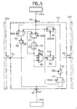
- FIG. 4 represents a cell of the type bidirectional 222 of conventional type to which we have made changes consistent with those of solutions envisaged in the bus type cell.
- This cell 222 includes a parallel input 302, a parallel output 322, a serial input 312, a serial output 332, a storage flip-flop 242 (by example of the master-slave delay type), a first locking latch 252, a second latch with lock 262, a first multiplexer 272 with two inputs, a second multiplexer 282 with three inputs, and a buffer circuit 292.
- the bidirectional cell 222 includes a third two-input multiplexer 342 having a input 0 connected to parallel input 302, its other input 1 connected to the output of the second flip-flop at lock 262, and an output connected to the input of the buffer circuit 292 whose output is connected to the parallel output 322.
- the parallel input 302 of cell 222 is connected to an input 0 of the first multiplexer 272.
- the input 312 series receives a binary Sin signal from a cell previous 222a from shift register 14 or terminal input 16 of shift register 14.
- This serial input 312 is connected to an input 1 of the second multiplexer 282.
- the serial output 332 is connected to the serial input of the next cell 222b, or at the output terminal 17 of the register 14 if it is the last cell in the register.
- the first multiplexer 272 has a connected output at the entrance to the first locking latch 252.
- This flip-flop 252 has its output connected on the one hand to a input 0 of the second multiplexer 282 and on the other hand to a second input 1 of the first multiplexer 272.
- the second multiplexer 282 has an output connected to the input of the storage flip-flop 242.
- This flip-flop 242 has its output connected to the serial output 332, to a input 2 of the second multiplexer 282 and at the input of the second locking lever 262.
- control signals necessary to make operate the cell are similar to those used for the unidirectional type cell. We will refer so to the description of this cell in what concerned.
- Parallel output 322 is connected to an input a fourth multiplexer 352 with two inputs having its other input connected to the scale output at lock 262 and an output connected to the input parallel 302, via a second buffer circuit 362 analogous to the first output buffer circuit 292.
- a bidirectional cell as defined above has the same advantages and disadvantages as the unidirectional cell described previously in this which concerns the characteristics of memorization, consumption, and propagation time.
- buffer circuits 292 and 362 three states, controlled by additional control signals ENO and / ENO, in order only one buffer circuit is running at a time. That would have the advantage of being certain of the meaning of signal propagation. Depending on the direction chosen and programmed, we could generate the control signals suitable for these three-state buffer circuits.
- Another benefit of using cells bidirectional three-state buffer circuit would be offer only one type of cell usable for unidirectional propagation lines without having to worry, at the time of their implementation, of the meaning of propagation to orient the cell (by cons it will be necessary to know this direction to produce the signals of ENO and / ENO command). That would simplify also implantation in the sense that all cells mounted in series on the lines unidirectional and bidirectional meaning of programmable propagation would then have identical characteristics (size, consumption, etc.).
- Flip-flop output 382 is connected to a fourth input of multiplexer 282 and this multiplexer receives an additional logic control signal S3, supplied by the test device 19, so that it can store in storage latch 242 as well the value of the signal present on the parallel input 302 than that present on the parallel output 322.
- This cell in Figure 6 therefore has the same features as that of Figure 4.
- multiplexer 272 is a three-way multiplexer starters.
- This multiplexer receives three control signals S'0, S'1 and S'2 logic to selectively supply on the output of this multiplexer, i.e. the signal present in output of the three-state buffer circuit 292, i.e. the signal present on parallel input 302, i.e. the signal present at the output of the locking latch 252.
Landscapes
- Engineering & Computer Science (AREA)
- General Engineering & Computer Science (AREA)
- Physics & Mathematics (AREA)
- General Physics & Mathematics (AREA)
- Tests Of Electronic Circuits (AREA)
- Shift Register Type Memory (AREA)
- Logic Circuits (AREA)
Claims (9)
- Integrierter Schaltkreis mit wenigstens einer Übertragungsleitung (231, 232) zwischen zwei Vorrichtungen (100, 200) und einer Schieberegisterzelle (221, 222), die in der Übertragungsleitung (231, 232) zwischen den zwei Vorrichtungen (100, 200) in Reihe geschaltet ist, um einen binären Wert auf wenigstens einen Leitungsabschnitt (231b, 232b) auszugeben, der mit einer der Vorrichtungen (200) verbunden ist, oder zum Abtasten des Wertes des Signals, das auf wenigstens einem Leitungsabschnitt (231a, 232a) anliegt, der mit einer der Vorrichtungen verbunden ist, wobei diese Zelle umfaßt:dadurch gekennzeichnet, daß er ein erstes Verriegelungs-Flip-Flop (251, 252) umfaßt, das über einen Eingang das parallele Eingangssignal (Pin) empfängt und das einen Ausgang hat, der mit dem ersten Eingang des ersten Multiplexers (281, 282) verbunden ist, wobei das erste Verriegelungs-Flip-Flop (251, 252) außerdem ein logisches Steuersignal (CLK) empfängt, um über den Ausgang das Signal, das am Eingang anliegt, zu verriegeln.einen parallelen Eingang (301, 302), der mit einem Leitungsabschnitt (231a, 232a) verbunden ist, welcher mit einer der Vorrichtungen (100) zum Empfangen eines parallelen Eingangssignals (Pin) verbunden ist,einen parallelen Ausgang (321, 322), der mit dem Teil der Leitung (232b) verbunden ist, welcher mit der anderen Vorrichtung (200) zum Ausgeben eines parallelen Ausgangssignals (Pout) verbunden ist,einen seriellen Eingang (311, 312) zum Empfangen eines seriellen Eingangssignals (Sin), um es in eine folgende Zelle (221b, 222b) zu verschieben oder auf die Leitung auszugeben,einen seriellen Ausgang (331, 332) zum Ausgeben eines seriellen Ausgangssignals (Sout) an einen seriellen Eingang einer folgenden Zelle,einen ersten Multiplexer (281, 282), der über einen ersten Eingang das parallele Eingangssignal (Pin) und über einen zweiten Eingang das serielle Eingangssignal (Sin) empfängt, wobei dieser erste Multiplexer (281, 282) einen Ausgang hat, der mit dem Eingang eines Speicher-Flip-Flops (241, 242) verbunden ist,einen zweiten Multiplexer (341, 342), der über einen ersten Eingang das parallele Eingangssignal (Pin) und über einen zweiten Eingang ein Signal zum Ausgeben auf den Teil der Leitung (232b) empfängt, mit dem der parallele Ausgang (322) verbunden ist,
- Schaltkreis nach Anspruch 1, dadurch gekennzeichnet, daß der parallele Eingang (302) mit einem ersten Eingang eines dritten Multiplexers (272) verbunden ist, wobei dieser dritte Multiplexer einen Ausgang, der mit dem Eingang des ersten Verriegelungs-Flip-Flops (252) verbunden ist, und einen zweiten Eingang umfaßt, der mit dem Ausgang dieses Verriegelungs-Flip-Flops verbunden ist.
- Schaltkreis nach einem der Ansprüche 1 oder 2, dadurch gekennzeichnet, daß der serielle Ausgang (332) einerseits mit dem Ausgang des Speicher-Flip-Flops (242) und andererseits mit einem dritten Eingang des ersten Multiplexers (282) verbunden ist.
- Schaltkreis nach einem der Ansprüche 1 bis 3, dadurch gekennzeichnet, daß er einen vierten Multiplexer (352) umfaßt, der an einem ersten Eingang das parallele Ausgangssignal (Pout) und an einem zweiten Eingang ein Signal zum Ausgeben auf den Teil der Leitung (232a), der mit dem parallelen Eingang (302) verbunden ist, empfängt.
- Schaltkreis nach Anspruch 4, dadurch gekennzeichnet, daß der zweite Multiplexer (342) mit dem parallelen Ausgang (322) über einen ersten Tristate-Zwischenschaltkreis (292) verbunden ist und daß der vierte Multiplexer (252) mit dem parallelen Eingang (302) über einen zweiten Tristate-Zwischenschaltkreis (362) verbunden ist.
- Schaltkreis nach Anspruch 5, dadurch gekennzeichnet, daß ein Ausgang des ersten Tristate-Zwischenschaltkreises (292) mit einem dritten Eingang des dritten Multiplexers (272) verbunden ist.
- Schaltkreis nach einem der Ansprüche 4 bis 6, dadurch gekennzeichnet, daß die zwei Eingänge des zweiten und vierten Multiplexers (342, 352) mit einem Ausgang eines zweiten Verriegelungs-Flip-Flops (262) verbunden sind, deren einer Eingang mit dem Speicher-Flip-Flop (242) verbunden ist.
- Schaltkreis nach einem der Ansprüche 4 bis 7, dadurch gekennzeichnet, daß er ein drittes Verriegelungs-Flip-Flop (382) umfaßt, das über einen Eingang das parallele Ausgangssignal (Pout) empfängt und das einen Ausgang umfaßt, der mit einem vierten Eingang des ersten Multiplexers (282) verbunden ist.
- Schaltkreis nach Anspruch 8, dadurch gekennzeichnet, daß er einen fünften Multiplexer (372) mit einem ersten Eingang, der mit dem parallelen Ausgang (322) verbunden ist, einem zweiten Eingang, der mit dem Ausgang des dritten Verriegelungs-Flip-Flops (382) verbunden ist, und mit einem Ausgang, der mit dem Eingang desselben Flip-Flops verbunden ist, umfaßt.
Applications Claiming Priority (3)
| Application Number | Priority Date | Filing Date | Title |
|---|---|---|---|
| FR9406491 | 1994-05-20 | ||
| FR9406491A FR2720205B1 (fr) | 1994-05-20 | 1994-05-20 | Cellule pour registre à décalage. |
| EP95470019A EP0686977B1 (de) | 1994-05-20 | 1995-05-12 | Zelle für Schieberegister |
Related Parent Applications (2)
| Application Number | Title | Priority Date | Filing Date |
|---|---|---|---|
| EP95470019A Division EP0686977B1 (de) | 1994-05-20 | 1995-05-12 | Zelle für Schieberegister |
| EP95470019.1 Division | 1995-05-12 |
Publications (3)
| Publication Number | Publication Date |
|---|---|
| EP0809255A2 EP0809255A2 (de) | 1997-11-26 |
| EP0809255A3 EP0809255A3 (de) | 1997-12-17 |
| EP0809255B1 true EP0809255B1 (de) | 1998-12-23 |
Family
ID=9463599
Family Applications (2)
| Application Number | Title | Priority Date | Filing Date |
|---|---|---|---|
| EP97111252A Expired - Lifetime EP0809255B1 (de) | 1994-05-20 | 1995-05-12 | Schieberegisterzelle |
| EP95470019A Expired - Lifetime EP0686977B1 (de) | 1994-05-20 | 1995-05-12 | Zelle für Schieberegister |
Family Applications After (1)
| Application Number | Title | Priority Date | Filing Date |
|---|---|---|---|
| EP95470019A Expired - Lifetime EP0686977B1 (de) | 1994-05-20 | 1995-05-12 | Zelle für Schieberegister |
Country Status (5)
| Country | Link |
|---|---|
| US (1) | US5589787A (de) |
| EP (2) | EP0809255B1 (de) |
| JP (1) | JPH0883164A (de) |
| DE (2) | DE69501481T2 (de) |
| FR (1) | FR2720205B1 (de) |
Families Citing this family (10)
| Publication number | Priority date | Publication date | Assignee | Title |
|---|---|---|---|---|
| US5744995A (en) * | 1996-04-17 | 1998-04-28 | Xilinx, Inc. | Six-input multiplexer wtih two gate levels and three memory cells |
| US5907562A (en) * | 1996-07-31 | 1999-05-25 | Nokia Mobile Phones Limited | Testable integrated circuit with reduced power dissipation |
| US6097889A (en) * | 1997-06-23 | 2000-08-01 | Motorola, Inc. | Signal processing apparatus with stages in a signal path operating as LFSR of alternable type and method for processing signals |
| US6219812B1 (en) * | 1998-06-11 | 2001-04-17 | Sun Microsystems, Inc. | Apparatus and method for interfacing boundary-scan circuitry with DTL output drivers |
| US6061417A (en) * | 1998-12-03 | 2000-05-09 | Xilinx, Inc. | Programmable shift register |
| US6434213B1 (en) * | 2001-03-08 | 2002-08-13 | Cirrus Logic, Inc. | Low-power low-area shift register |
| KR100594317B1 (ko) | 2005-01-28 | 2006-06-30 | 삼성전자주식회사 | 소비전력이 적은 쉬프트 레지스터 및 상기 쉬프트레지스터의 동작방법 |
| US7242235B1 (en) * | 2005-02-25 | 2007-07-10 | Exar Corporation | Dual data rate flip-flop |
| US7554858B2 (en) * | 2007-08-10 | 2009-06-30 | Micron Technology, Inc. | System and method for reducing pin-count of memory devices, and memory device testers for same |
| US8700845B1 (en) * | 2009-08-12 | 2014-04-15 | Micron Technology, Inc. | Daisy chaining nonvolatile memories |
Family Cites Families (7)
| Publication number | Priority date | Publication date | Assignee | Title |
|---|---|---|---|---|
| US4722049A (en) * | 1985-10-11 | 1988-01-26 | Unisys Corporation | Apparatus for out-of-order program execution |
| US4701921A (en) * | 1985-10-23 | 1987-10-20 | Texas Instruments Incorporated | Modularized scan path for serially tested logic circuit |
| US4872137A (en) * | 1985-11-21 | 1989-10-03 | Jennings Iii Earle W | Reprogrammable control circuit |
| US4970690A (en) * | 1989-07-31 | 1990-11-13 | Atari Games Corporation | Memory cell arrangement supporting bit-serial arithmetic |
| JP2535670B2 (ja) * | 1991-01-28 | 1996-09-18 | 株式会社東芝 | 双方向入出力端子用バウンダリスキャンセル |
| US5202625A (en) * | 1991-07-03 | 1993-04-13 | Hughes Aircraft Company | Method of testing interconnections in digital systems by the use of bidirectional drivers |
| FR2693574B1 (fr) * | 1992-07-08 | 1994-09-09 | Sgs Thomson Microelectronics | Procédé pour tester le fonctionnement d'un circuit intégré spécialisé, et circuit intégré spécialisé s'y rapportant. |
-
1994
- 1994-05-20 FR FR9406491A patent/FR2720205B1/fr not_active Expired - Fee Related
-
1995
- 1995-05-12 EP EP97111252A patent/EP0809255B1/de not_active Expired - Lifetime
- 1995-05-12 DE DE69501481T patent/DE69501481T2/de not_active Expired - Fee Related
- 1995-05-12 DE DE69506918T patent/DE69506918T2/de not_active Expired - Fee Related
- 1995-05-12 EP EP95470019A patent/EP0686977B1/de not_active Expired - Lifetime
- 1995-05-18 US US08/443,808 patent/US5589787A/en not_active Expired - Lifetime
- 1995-05-22 JP JP7146775A patent/JPH0883164A/ja not_active Withdrawn
Also Published As
| Publication number | Publication date |
|---|---|
| EP0686977A1 (de) | 1995-12-13 |
| DE69506918D1 (de) | 1999-02-04 |
| FR2720205B1 (fr) | 1996-07-12 |
| DE69506918T2 (de) | 1999-05-12 |
| EP0686977B1 (de) | 1998-01-21 |
| DE69501481T2 (de) | 1998-04-30 |
| US5589787A (en) | 1996-12-31 |
| EP0809255A2 (de) | 1997-11-26 |
| FR2720205A1 (fr) | 1995-11-24 |
| JPH0883164A (ja) | 1996-03-26 |
| EP0809255A3 (de) | 1997-12-17 |
| DE69501481D1 (de) | 1998-02-26 |
Similar Documents
| Publication | Publication Date | Title |
|---|---|---|
| FR2827684A1 (fr) | Controleur de memoire presentant une capacite d'ecriture 1x/mx | |
| EP0809255B1 (de) | Schieberegisterzelle | |
| FR2839156A1 (fr) | Circuit et procede utilisant de multiples chaines d'acces serie pour le test de cirucuits integres | |
| EP0683454B1 (de) | Verfahren zur Überwachung des Programmablaufs | |
| FR2587124A1 (fr) | Procede pour tester des supports portant plusieurs circuits integres a fonctionnement numerique, support pourvu de tels circuits, circuit integre propre a etre monte sur un tel support et dispositif de test pour tester de tels supports | |
| EP0887653A1 (de) | Verfahren zur Funktionsprüfung und Schaltung mit Mitteln zum Durchführen dieses Verfahrens | |
| FR2701120A1 (fr) | Appareil de test de mémoire. | |
| FR2492107A1 (fr) | Dispositif d'essai de pastille d'integration poussee, forme sur la meme pastille | |
| FR2860313A1 (fr) | Composant a architecture reconfigurable dynamiquement | |
| FR2667706A1 (fr) | Antememoire hierarchique a circuits integres. | |
| FR2985358A1 (fr) | Chaine de balayage en peripherie pour memoire en pile | |
| EP0578540B1 (de) | Verfahren zur Prüfung der Funktionsfähigkeit einer ASIC-Schaltung und darauf bezogene ASIC-Schaltung | |
| FR2849228A1 (fr) | Dispositif de transfert de donnees entre deux sous-systemes asynchrones disposant d'une memoire tampon | |
| EP0648017B1 (de) | Vorrichtung zur Überwachung der Phasenverschiebung zwischen zwei Taktsignalen | |
| FR2632092A1 (fr) | Circuit de conditionnement d'ecriture d'antememoire retarde pour un systeme de microcalculateur a bus double comprenant une unite 80386 et une unite 82385 | |
| FR2595474A1 (fr) | Dispositif de controle et de verification du fonctionnement de blocs internes a un circuit integre | |
| FR2718272A1 (fr) | Mémoire vive vidéo et procédé pour fournir en sortie des données série. | |
| EP1159628B1 (de) | Verfahren zur prüfung von integrierten schaltungen mit speicherelement-zugriff | |
| EP0733975B1 (de) | Ausgangschnittstelle für binäre Daten | |
| FR2890766A1 (fr) | Systeme et procede de communication asynchrone sur circuit, entre des sous-circuits synchrones | |
| FR3134462A1 (fr) | Procédé de transfert de données entre un premier domaine numérique et un deuxième domaine numérique, et système sur puce correspondant. | |
| EP0464768B1 (de) | Schnittstellenmodul für Datenübertragung | |
| EP0025731A1 (de) | Auswahlschaltung für asynchronen Anforderungen in einem Datenverarbeitungssystem | |
| EP0683455B1 (de) | Mikrocomputer mit integrierter Haltepunktanordnung zur Erkennung von zusammengesetzten Ereignissen | |
| EP2208143B1 (de) | Struktur und verfahren für speicherung und abruf von daten |
Legal Events
| Date | Code | Title | Description |
|---|---|---|---|
| PUAI | Public reference made under article 153(3) epc to a published international application that has entered the european phase |
Free format text: ORIGINAL CODE: 0009012 |
|
| PUAL | Search report despatched |
Free format text: ORIGINAL CODE: 0009013 |
|
| AC | Divisional application: reference to earlier application |
Ref document number: 686977 Country of ref document: EP |
|
| AK | Designated contracting states |
Kind code of ref document: A2 Designated state(s): DE FR GB IT |
|
| AK | Designated contracting states |
Kind code of ref document: A3 Designated state(s): DE FR GB IT |
|
| 17P | Request for examination filed |
Effective date: 19971231 |
|
| GRAG | Despatch of communication of intention to grant |
Free format text: ORIGINAL CODE: EPIDOS AGRA |
|
| 17Q | First examination report despatched |
Effective date: 19980318 |
|
| GRAG | Despatch of communication of intention to grant |
Free format text: ORIGINAL CODE: EPIDOS AGRA |
|
| GRAH | Despatch of communication of intention to grant a patent |
Free format text: ORIGINAL CODE: EPIDOS IGRA |
|
| GRAH | Despatch of communication of intention to grant a patent |
Free format text: ORIGINAL CODE: EPIDOS IGRA |
|
| GRAA | (expected) grant |
Free format text: ORIGINAL CODE: 0009210 |
|
| AC | Divisional application: reference to earlier application |
Ref document number: 686977 Country of ref document: EP |
|
| AK | Designated contracting states |
Kind code of ref document: B1 Designated state(s): DE FR GB IT |
|
| GBT | Gb: translation of ep patent filed (gb section 77(6)(a)/1977) |
Effective date: 19981223 |
|
| RAP4 | Party data changed (patent owner data changed or rights of a patent transferred) |
Owner name: STMICROELECTRONICS S.A. |
|
| REF | Corresponds to: |
Ref document number: 69506918 Country of ref document: DE Date of ref document: 19990204 |
|
| ITF | It: translation for a ep patent filed | ||
| PLBE | No opposition filed within time limit |
Free format text: ORIGINAL CODE: 0009261 |
|
| STAA | Information on the status of an ep patent application or granted ep patent |
Free format text: STATUS: NO OPPOSITION FILED WITHIN TIME LIMIT |
|
| 26N | No opposition filed | ||
| REG | Reference to a national code |
Ref country code: GB Ref legal event code: IF02 |
|
| PGFP | Annual fee paid to national office [announced via postgrant information from national office to epo] |
Ref country code: DE Payment date: 20040520 Year of fee payment: 10 |
|
| PGFP | Annual fee paid to national office [announced via postgrant information from national office to epo] |
Ref country code: GB Payment date: 20050511 Year of fee payment: 11 Ref country code: FR Payment date: 20050511 Year of fee payment: 11 |
|
| PG25 | Lapsed in a contracting state [announced via postgrant information from national office to epo] |
Ref country code: IT Free format text: LAPSE BECAUSE OF NON-PAYMENT OF DUE FEES;WARNING: LAPSES OF ITALIAN PATENTS WITH EFFECTIVE DATE BEFORE 2007 MAY HAVE OCCURRED AT ANY TIME BEFORE 2007. THE CORRECT EFFECTIVE DATE MAY BE DIFFERENT FROM THE ONE RECORDED. Effective date: 20050512 |
|
| PG25 | Lapsed in a contracting state [announced via postgrant information from national office to epo] |
Ref country code: DE Free format text: LAPSE BECAUSE OF NON-PAYMENT OF DUE FEES Effective date: 20051201 |
|
| PG25 | Lapsed in a contracting state [announced via postgrant information from national office to epo] |
Ref country code: GB Free format text: LAPSE BECAUSE OF NON-PAYMENT OF DUE FEES Effective date: 20060512 |
|
| GBPC | Gb: european patent ceased through non-payment of renewal fee |
Effective date: 20060512 |
|
| REG | Reference to a national code |
Ref country code: FR Ref legal event code: ST Effective date: 20070131 |
|
| PG25 | Lapsed in a contracting state [announced via postgrant information from national office to epo] |
Ref country code: FR Free format text: LAPSE BECAUSE OF NON-PAYMENT OF DUE FEES Effective date: 20060531 |