EP1159628B1 - Verfahren zur prüfung von integrierten schaltungen mit speicherelement-zugriff - Google Patents
Verfahren zur prüfung von integrierten schaltungen mit speicherelement-zugriff Download PDFInfo
- Publication number
- EP1159628B1 EP1159628B1 EP00909440A EP00909440A EP1159628B1 EP 1159628 B1 EP1159628 B1 EP 1159628B1 EP 00909440 A EP00909440 A EP 00909440A EP 00909440 A EP00909440 A EP 00909440A EP 1159628 B1 EP1159628 B1 EP 1159628B1
- Authority
- EP
- European Patent Office
- Prior art keywords
- boundary scan
- scan chain
- integrated circuit
- inputs
- outputs
- Prior art date
- Legal status (The legal status is an assumption and is not a legal conclusion. Google has not performed a legal analysis and makes no representation as to the accuracy of the status listed.)
- Expired - Lifetime
Links
Images

Classifications
-
- G—PHYSICS
- G01—MEASURING; TESTING
- G01R—MEASURING ELECTRIC VARIABLES; MEASURING MAGNETIC VARIABLES
- G01R31/00—Arrangements for testing electric properties; Arrangements for locating electric faults; Arrangements for electrical testing characterised by what is being tested not provided for elsewhere
- G01R31/28—Testing of electronic circuits, e.g. by signal tracer
- G01R31/317—Testing of digital circuits
- G01R31/3181—Functional testing
- G01R31/3185—Reconfiguring for testing, e.g. LSSD, partitioning
- G01R31/318533—Reconfiguring for testing, e.g. LSSD, partitioning using scanning techniques, e.g. LSSD, Boundary Scan, JTAG
- G01R31/318536—Scan chain arrangements, e.g. connections, test bus, analog signals
-
- G—PHYSICS
- G01—MEASURING; TESTING
- G01R—MEASURING ELECTRIC VARIABLES; MEASURING MAGNETIC VARIABLES
- G01R31/00—Arrangements for testing electric properties; Arrangements for locating electric faults; Arrangements for electrical testing characterised by what is being tested not provided for elsewhere
- G01R31/28—Testing of electronic circuits, e.g. by signal tracer
- G01R31/317—Testing of digital circuits
- G01R31/3181—Functional testing
- G01R31/3185—Reconfiguring for testing, e.g. LSSD, partitioning
- G01R31/318533—Reconfiguring for testing, e.g. LSSD, partitioning using scanning techniques, e.g. LSSD, Boundary Scan, JTAG
- G01R31/318572—Input/Output interfaces
Definitions
- the present invention relates to methods and devices for test the integrated circuits as well as the integrated circuits provided with means authorizing effective tests.
- a first process called “automatic generation process test vectors per full scan path ", or” full scan ATPG "in English, is commonly used to test the manufacture of fleas.
- This process consists in injecting pins of the integrated circuit with known signals and to take the values obtained from the output pins, to compare them to expected values.
- This first method has a major drawback.
- testers are more expensive than their number of channels is high.
- FIG. 3 shows a circuit tested with this known process, on which are indicated by the reference 10 the branches not connected, and on which the untested areas have been hatched.
- JTAG Boundary scan of the periphery
- IEEE standard 1149.1 essentially concerns the testing of printed cards and soldering of integrated circuits on these cards.
- This IEEE 1149.1 standard provides an access / entry path suitable for replacing a direct physical connection to the inputs / outputs.
- This second type of test is implemented by adding to the circuit integrated and in the printed card which carries it a specific logic for this test which allows, under the control of a PLC called TAP controller ("Test Access Port controller ", to capture the logical level present on an input, and / or to impose the logic level on an output of the circuit integrated. In normal mode, this logic is transparent, both for inputs only for outputs.
- the integrated circuits of a card are provided with a path access having the form of a loop and connecting in series all of the inputs / outputs of the circuit considered, and the loops of each of the circuits integrated are connected in series.
- the Boundary Scan chain therefore traverses the component to which it is integrated, and also traverses the card receiving the components.
- a general Boundary Scan chain connects the chains of Boundary Scan of each component, so that each pad input / output of each component as well as each track of the card is accessible from outside the map, by the same path from a specific terminal of the card, transfer of data captured or to to impose taking place in series on this path.
- the Boundary Scan also authorizes to test the interconnections between the integrated circuits on a card.
- the test vector is loaded in series in the Boundary path scan, then sent to the interconnects to be tested via output buffers components.
- the results are sampled in the Boundary scan, via the component inputs, then output in series to the tester.
- test vector is loaded in series in the path of Boundary Scan then applied to the internal logic of the integrated circuit. The result is sampled in the Boundary Scan Path, then read in series by the tester.
- This second test method has drawbacks: particularly long implementation, especially in the internal mode where we test the components of the card.
- this test method turns out particularly unsuitable for testing integrated circuits before mounting, in particular for testing integrated circuits comprising elements of storage.
- the object of the invention is to resolve these various drawbacks, by proposing an integrated circuit test method which does not require the connection of all the inputs / outputs of this circuit to a tester and to test a large area, or even the entire circuit, this process which can also be carried out much faster than known test methods.
- the invention proposes to improve the coverage of an integrated circuit manufacturing test compared to the known method full-scan ATPG, without increasing the number of channels of the tester.
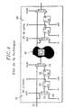
- the two modules 20 and 30 shown here are identical, one to the other.Each of the two modules 20 and 30 is placed in parallel with one direct connection between a connection pin and the core 40 of the chip.
- module 20 module 30 comprising the same elements as module 20.
- the module 20 has two ends, each formed by a multiplexer 22, 24.
- a first 22 of these two multiplexers receives on a link 23 a control signal called “signal shift”, which configures the cell in “shift” or in “loading”.
- the multiplexer 22 is capable of receiving a signal from its first input 21 pin, which is for example a signal received from another chip on the card
- the latter On a second input 23 of the multiplexer 22, the latter receives a input signal SI, carrying data transferred in the chain Boundary Scan and intended to be loaded by cell 20 if it is in "shift" mode.
- the cell has two registers 25 and 26, one of which is a shift register 25 which delivers a SO output signal to be passed in the Boundary Scan to other input / output cells not shown on chip 40, or else to other chips.
- the shift register 25 also receives a clock signal noted ck and the other register 26 receives an upd signal for updating the locks of output from cell 20, that is to say memories from cell 20 capable of form a selected logic level of this input or this output of the circuit integrated, when this cell 20 is activated.
- the shift register 25 also delivers a signal SO which contains, for certain cells, information recorded on this cell and / or representative of data recorded in cell 20, possibly intended to be analyzed to interpret the test.
- Sl is therefore the serial data input, SO the output of serial data.
- the multiplexer 24 located at the other end of the cell 20 is at say between cell 20 and core 40 of the chip, receives a "mode" signal able to control cell 20 so that the signal transmitted by cell 20 at the heart of chip 40 is not the signal received on pin 21 but the signal consisting of the contents of the locks of cell 20.
- the signals SI and SO pass through the integrated circuit, from cell input / output in the input / output cell on the entire loop Boundary scan connecting these inputs / outputs in series.
- such an integrated circuit includes a controller TAP, not shown, whose role is to generate the control signals SHIFT, UPD, CK and MODE of the Boundary Scan chain of the integrated circuit.
- the TAP controller When testing a card, the TAP controller itself receives control signals flowing in the Boundary scan path of the menu. These control signals transmit to the circuit TAP controller the instructions concerning logical levels to be imposed on certain cells of its integrated circuit. Conversely, the TAP controller transmits also in the path of Boundary scan of the logical levels noted on certain cells.
- the integrated circuit according to the invention which is shown in FIG. 5, has a set of pins 100, each associated with a cell input / output 110.
- the 110 cells are connected in series by a path Boundary Scan device 120, shown in double dashed lines. This peripheral path 120 therefore forms a loop 110 which traverses the perimeter of the input / output cell circuit 110 in input / output cell 110.
- This integrated circuit includes combinatorial functions 130 and storage elements 140.
- the storage elements 140 are linked together in series by a path 150 which provides access to these memories from an external pin 108. This path 150 makes it possible to control, during a test, memories 140 directly from outside the circuit.
- pins 110 some pins referenced 103 are connected to the channels of a not shown tester and other pins referenced 105 are not connected to the tester.
- the pins connected 103 are extended in FIG. 5 by a bold line, while the unconnected pins 105 have only a short thin line.
- the test of this integrated circuit is carried out by acting from the outside on the memories 140, while activating the 120 Boundary Scan Road.
- path 150 we use the path 150 or to place the memories 140 in a predetermined state, or to record their state during the test. Simultaneously, we use path 120 of Boundary scan to impose on some inputs / outputs not connected 105 the logic levels predetermined or to identify logical levels to be observed.
- injected into the pins connected 103 signals chosen directly through the channels of the tester.
- the tester Since the Boundary Scan 120 path is connected to the tester, the tester sends in this path a signal chosen specifically to activate some of the other 105 cells that are unconnected and for their impose a predetermined logic level.
- the invention also provides for not acting directly on any pin and to impose or read the logic levels of the inputs / outputs only through the Boundary Scan, while acting directly on the memory elements 140 of the circuit by one or more direct accesses to these briefs 140.
- the access path 150 memory items 140 is concatenated at Boundary Scan path 120 so that these two paths form the same chain on which the memory elements 140 and the cells are placed in series input / output 110.
- FIG 6 there is shown an assembly adapted to such a concatenation of the Boundary Scan 120 chain and the 150 chain direct access to memories 140.
- This preferred arrangement presents the advantage of leaving the Boundary Scan 120 path available at TAP controller outside of an implementation of the test method according to the invention and to allow, during a test of the integrated circuit carried out according to the invention, to activate the path of Boundary Scan 120.
- the access chain 150 to memories 140 is connected to the Boundary Scan 120 chain via at least one multiplexer controlled by an ATPG-mode mode signal, injected from the pin 108.
- Boundary Scan 120 chain includes six bonds.
- Figure 6 the path of Boundary Scan 120 by a simple rectangle provided with six connections corresponding to these links.
- This connection is located downstream of the TAP 200 controller on the Boundary Scan chain and downstream of storage points 140 on the path 150.
- the pin 108 forms the outer end of a set of four links running parallel to each other on path 150 to this junction.
- the ATPG-mode link is connected to five multiplexers (or equivalent functions) of which it constitutes each time a channel of ordered.
- a first multiplexer 210 receives on a first input the SI signal carried on the ATPG-Si link and receives on a second input a input signal Sl from the TAP 200 controller.
- a second multiplexer 220 receives on its two inputs respectively the clock signal CK coming from pin 108 and another CK clock signal from controller 200.
- a third multiplexer 230 receives on its inputs respectively the signal SE from pin 108 and the signal SHIFT from controller 200.
- a fourth multiplexer 240 receives on its two inputs respectively the mode signal from the controller 200 and a signal constant activation noted "1".
- a fifth multiplexer 250 receives on its two inputs respectively the UPD update signal from the controller 200 and a constant activation signal noted "1".
- the Boundary Scan 120 is connected to its device 200 command provided to perform a current Boundary Scan test.
- Boundary channels SI, CK, SHIFT Scan 120 are respectively connected to the signals SI, CK, SE applied respectively on the ATPG-Si, Clock and ATPG-Se links of the spindle 108, while the MODE and UPD links of the Boundary Scan 120 are related to the constant activation values equal to 1.
- the Boundary Scan path 120 and the 110 cells it includes are controlled by the signals SI, CK, and SE applied to the pin 108 from the outside.
- the MODE signal and the UPD signal received by the Boundary Scan 120 chain are the permanent activation signals of so that the contents of the locks of the Boundary input / output cells Scan replaces the signals normally taken from the pins of these cells during the test according to the invention.
- the access path 150 to the memories 140 is connected permanently at the clock input of pin 108, unlike the Boundary Scan 120 which is subject to the clock signal from controller 200 or pin 108 depending on the content of the mode signal applied to the pin 108.
- the output of the Boundary Scan 120 chain forms a pin 109 and also carries a link connecting this pin 109 to the controller 200, so that on the controller 200 the SO output signal is looped back of the Boundary Scan 120.
- a tester connected to the inputs ATPG-Se, Clock, ATPG-mode and ATPG-Si of pin 108 activates the chain concatenated comprising the memories 140 in series with the cells 110, and applies a selected state to memories 140, imposes a selected signal on 100 selected inputs / outputs of the integrated circuit through the Boundary Scan chain, and detects signals obtained on inputs / outputs 100 of the integrated circuit through the chain Boundary Scan 120, as well as pin 109.
- the tester is advantageously provided with a few channels connected directly to input / output pins 100 of the circuit.
- the tester then includes a module to directly inject in input-output connected to these channels of the test signals and for receive signals coming out of these inputs-outputs 100, and for them compare to expected signals.
- the tester then includes a device for control of the Boundary Scan 120 chain of the integrated circuit which is coordinated with the direct injection / reception module to generate test vectors on sets comprising both input-output 103 connected directly to the tester and both I / O 105 connected to the tester via the Boundary Scan 120 chain.
- the test allows testing all parts of the circuit and is particularly fast, efficient, especially because we use a tester that has a acceptable number of channels and allows a quick and more complete test of the circuit.
- the number of control points is increased and observation, and therefore we improve the test coverage in the vicinity of inputs-outputs left unconnected.
- the invention improves testability in the vicinity of input-output bidirectional, even those connected to a tester channel, because it provides test access to an intermediate point which according to the IEEE standard 1149.1 must be part of the Boundary Scan chain, namely the signal of direction.
Claims (21)
- Verfahren zum Testen einer integrierten Schaltung, die Speicherstellen (140) und eine Boundary Scan Chain (120) umfaßt, in die geschrieben wird und/oder gelesen wird auf den Speicherscellen (140) mittels eines Zugriffspfades (150) zu den Speicherstellen (140) von einem Außenanschluß (108) der Schaltung, dadurch gekennzeichnet, daß die Boundary Scan Chain (120) aktiviert wird, um logische Pegel an den Eingängen/Ausgängen (110) der integrierten Schaltung anzulegen und/oder zu beobachten.
- Verfahren nach Anspruch 1, dadurch gekennzeichnet, daß der Zugriffspfad (150) zu den Speicherstellen (140) und die Boundary Scan Chain (120) gleichzeitig aktiv sind.
- Verfahren nach Anspruch 1 oder 2, dadurch gekennzeichnet, daß der Zugriffspfad (150) zu den Speicherstellen (140) und die Boundary Scan Chain mittels einer Leitung aktiviert werden, die in Serie den Zugriffspfad (150) zu den Speicherstellen (140) und die Boundary Scan Chain (120) umfaßt.
- Verfahren nach einem der Ansprüche 1 bis 3, dadurch gekennzeichnet, daß die Boundary Scan Chain (120) mittels eines Aktivierungspfades (150) aktiviert wird, der mit der Boundary Scan Chain (120) stromab einer TAP-Steuerung (200) verbunden ist.
- Verfahren nach Anspruch 4, dadurch gekennzeichnet, daß der Aktivierungspfad (150) mit der Boundary Scan Chain (120) wenigstens über ein logisches Gatter (210, 220, 230, 240, 250) verbunden ist, das geeignet ist, abhängig von einem Steuersignal (ATPG-Modus) die Boundary Scan Chain (120) entweder mit dem Aktivierungspfad (150) der Boundary Chain oder mit der TAP-Steuerung (200) zu verbinden.
- Verfahren nach einem der Ansprüche 4 oder 5, dadurch gekennzeichnet, daß der Aktivierungspfad (150) wenigstens einen Kanal (ATPG-Si) aufweist, auf dem wenigstens eine Speicherstelle (140) angeordnet ist, wobei dieser Kanal geeignet ist, in Serie mit der Boundary Scan Chain (120) verbunden zu werden, wenn diese aktiviert ist.
- Verfahren nach einem der vorhergehenden Ansprüche, dadurch gekennzeichnet, daß die Eingangs- (Si), Takt- (ck) und Konfigurations-Kanäle (Sc) der Boundary Scan Chain (120) mit logischen Gattern (210, 220, 230, 240, 250) verbunden sind, die geeignet sind, gemäß einem Steuersignal (ATPG-Modus) diese Signale (Si, ck, Sh) entweder mit den Eingangs- (Si), Takt- (ck) und Konfigurations-Kanälen (Sh) der Steuerung TAP (200) oder mit den Eingangs- (Si), Takt- (ck) und Konfigurations-Kanälen (Sh) des Aktivierungspfades (150) zu verbinden.
- Verfahren nach einem der vorhergehenden Ansprüche, dadurch gekennzeichnet, daß alle Speicherstellen (140) in Serie geschaltet sind.
- Verfahren nach einem der vorhergehenden Ansprüche, dadurch gekennzeichnet, daß wenigstens ein Teil der Eingänge/Ausgänge (110) der integrierten Schaltung direkt mit einem Testgerät verbunden ist, das geeignet ist, ausgewählte Signale direkt in einige dieser Eingänge/Ausgänge (110) einzugeben, und/oder Ausgangssignale direkt von einigen dieser Eingänge/Ausgänge (110) zu empfangen und diese Ausgangssignale mit erwarteten Signalen zu vergleichen.
- Verfahren nach einem der vorhergehenden Ansprüche, in Kombination mit Anspruch 9, dadurch gekennzeichnet, daß das Testgerät zum direkten Eingeben und/oder direkten Messen einer Steuervorrichtung der Boundary Scan Chain (120) zum Erzeugen von Testvektoren auf Mengen zugeordnet ist, die zugleich mit dem Testgerät direkt verbundene Eingänge/Ausgänge (103) und zugleich mit dem Testgerät über die Boundary Scan Chain (120) verbundene Eingänge/Ausgänge (105) umfassen.
- Verfahren nach einem der vorhergehenden Ansprüche, dadurch gekennzeichnet, daß die Schaltung Zugriff (150) auf die Menge ihrer Speicherstellen (140) aufweist, und daß der Test unter Steuerung der Menge an speicherstellen (140) derart durchgeführt wird, daß die Funktion der integrierten Schaltung sich auf eine kombinatorische Funktion reduziert.
- Integrierte Schaltung, die eine Boundary Scan Chain (120) und einen Zugriffspfad (150) zu wenigstens einer Speicherstelle (140) umfaßt, dadurch gekennzeichnet, daß der Zugriffspfad (150) und die Boundary Scan Chain (120) in Serie geschaltet sind, und daß die Schaltung Mittel (220, 230, 240, 250) zum gleichzeitigen Eingreifen in die Speicherstelle(n) (140) des Zugriffspfades (150) und in die Zellen (110) der Boundary Scan Chain (120) aufweist.
- Integrierte Schaltung nach Anspruch 12, dadurch gekennzeichnet, daß die Mittel (220, 230, 240, 250) zum gleichzeitigen Eingreifen in die Speicherstelle(n) (140) des Zugriffspfades (150) und in die Zellen (110) der Boundary Scan Chain (120) wenigstens ein logisches Gatter (220, 230, 240, 250) umfassen, das geeignet ist, die Boundary Scan Chain (120) entweder mit dem Zugriffspfad (150) oder mit einer TAP-Steuerung (200) zu verbinden.
- Integrierte Schaltung nach Anspruch 12 oder 13, dadurch gekennzeichnet, daß die Eingangs- (Si), Takt- (CK) und Konfigurations-Kanäle (SHIFT) der Boundary Scan Chain (120) mit logischen Gattern (220, 230, 240, 250) verbunden sind, die geeignet sind, gemäß einem Steuersignal (MODE) diese Kanäle entweder mit den Eingangs- (SI), Takt- (CK) und Konfigurations-Kanälen (SHIFT) der TAP-Steuerung (200) oder mit den Eingangs- (ATPG_si), Takt- (ATPG_ck) und Konfigurations-Kanälen (ATPG_se) des Zugriffspfades (150) zu verbinden.
- Integrierte Schaltung nach einem der Ansprüche 12 bis 14, dadurch gekennzeichnet, daß alle Speichersteilen (140) der integrierten Schaltung in Serie geschaltet sind.
- Testgerät für integrierte Schaltungen, das ein erstes Modul zum Anlegen und/oder Lesen von Zuständen von Speicherstellen (140) einer integrierten Schaltung umfaßt, dadurch gekennzeichnet, daß es ein zweites Modul zum Anlegen von Zuständen und/oder Lesen von Zuständen von Eingangs-/Ausgangszellen (110) mittels der Boundary Scan Chain (120) der Schaltung gleichzeitig mit der Aktion des ersten Moduls umfaßt.
- Testgerät für integrierte Schaltungen nach Anspruch 16, dadurch gekennzeichnet, daß es zum gleichzeitigen Eingeben von Steuersignalen (SI) von Speicherstellen (140) und von Steuersignalen (SI) von Eingängen/Ausgängen (110) der Boundary Scan (120) in eine integrierte Schaltung vorgesehen ist.
- Testgerät nach Anspruch 17, dadurch gekennzeichnet, daß es zum Eingeben der Steuersignale (51) der Speicherstellen (140) und der Steuersignale (51) der Eingänge/Ausgänge (110) der Boundary Scan (120) in den gleichen Kanal vorgesehen ist.
- Testgerät nach einem der Ansprüche 16 bis 18, dadurch gekennzeichnet, daß es eine Reihe von Kanälen umfaßt, die geeignet sind, direkt mit Eingängen/Ausgängen (103) einer integrierten Schaltung verbunden zu werden, und ein Modul, das geeignet ist, ausgewählte Signale direkt in einige dieser Eingänge/Ausgänge (103) einzugeben und/oder Ausgangssignale von diesen Eingängen/Ausgängen (103, 109) zu empfangen, um diese Ausgangssignale mit erwarteten Signalen zu vergleichen.
- Testgerät nach Anspruch 19, dadurch gekennzeichnet, daß es eine Steuervorrichtung der Boundary Scan Chain (120) einer integrierten Schaltung, die dem Direkt-Eingabe/Empfang-Modul zugeordnet ist, aufweist, um Teetvektoren auf Mengen zu erzeugen, die zugleich mit dem Testgerät direkt verbundene Eingänge-Ausgänge (103) und zugleich mit dem Testgerät über die Boundary Scan Chain (120) verbundene Eingänge-Ausgänge (105) umfassen.
- Testgerät nach einem der Ansprüche 16 bis 20, dadurch gekennzeichnet, daß es geeignet ist, die Menge der Speicherstellen (140) derart zu steuern, daß sich die Funktion der integrierten Schaltung auf eine kombinatorische Funktion während des Test reduziert.
Applications Claiming Priority (3)
| Application Number | Priority Date | Filing Date | Title |
|---|---|---|---|
| FR9902823 | 1999-03-08 | ||
| FR9902823A FR2790832B1 (fr) | 1999-03-08 | 1999-03-08 | Procede de test de circuits integres avec acces a des points de memorisation du circuit |
| PCT/FR2000/000559 WO2000054067A1 (fr) | 1999-03-08 | 2000-03-07 | Procede de test de circuits integres avec acces a des points de memorisation du circuit |
Publications (2)
| Publication Number | Publication Date |
|---|---|
| EP1159628A1 EP1159628A1 (de) | 2001-12-05 |
| EP1159628B1 true EP1159628B1 (de) | 2002-12-18 |
Family
ID=9542925
Family Applications (1)
| Application Number | Title | Priority Date | Filing Date |
|---|---|---|---|
| EP00909440A Expired - Lifetime EP1159628B1 (de) | 1999-03-08 | 2000-03-07 | Verfahren zur prüfung von integrierten schaltungen mit speicherelement-zugriff |
Country Status (5)
| Country | Link |
|---|---|
| US (1) | US6886122B1 (de) |
| EP (1) | EP1159628B1 (de) |
| FR (1) | FR2790832B1 (de) |
| TW (1) | TW536635B (de) |
| WO (1) | WO2000054067A1 (de) |
Families Citing this family (8)
| Publication number | Priority date | Publication date | Assignee | Title |
|---|---|---|---|---|
| US7313739B2 (en) * | 2002-12-31 | 2007-12-25 | Analog Devices, Inc. | Method and apparatus for testing embedded cores |
| JP4579230B2 (ja) * | 2003-02-10 | 2010-11-10 | エヌエックスピー ビー ヴィ | 集積回路の試験 |
| EP1810044B1 (de) | 2004-07-28 | 2009-04-29 | Nxp B.V. | Schaltungsverbindungs-prüfanordnung und ansatz dafür |
| US7555687B2 (en) * | 2005-07-20 | 2009-06-30 | Texas Instruments Incorporated | Sequential scan technique for testing integrated circuits with reduced power, time and/or cost |
| US7301836B1 (en) * | 2005-10-25 | 2007-11-27 | Altera Corporation | Feature control circuitry for testing integrated circuits |
| US20080282120A1 (en) * | 2007-05-11 | 2008-11-13 | Macronix International Co., Ltd. | Memory structure, repair system and method for testing the same |
| US8533548B2 (en) * | 2010-11-11 | 2013-09-10 | Wisconsin Alumni Research Foundation | Wrapper cell for hierarchical system on chip testing |
| CN112462245B (zh) * | 2019-09-09 | 2022-08-19 | 英业达科技有限公司 | 边界扫描互联线路的生成方法与装置 |
Family Cites Families (6)
| Publication number | Priority date | Publication date | Assignee | Title |
|---|---|---|---|---|
| US6085336A (en) * | 1987-06-02 | 2000-07-04 | Texas Instruments Incorporated | Data processing devices, systems and methods with mode driven stops |
| DE68921269T2 (de) * | 1988-09-07 | 1995-06-22 | Texas Instruments Inc | Integrierte Prüfschaltung. |
| US5509019A (en) * | 1990-09-20 | 1996-04-16 | Fujitsu Limited | Semiconductor integrated circuit device having test control circuit in input/output area |
| US5850513A (en) * | 1996-01-05 | 1998-12-15 | Unisys Corporation | Processor path emulation system providing fast readout and verification of main memory by maintenance controller interface to maintenance subsystem |
| US5701308A (en) * | 1996-10-29 | 1997-12-23 | Lockheed Martin Corporation | Fast bist architecture with flexible standard interface |
| GB9622686D0 (en) * | 1996-10-31 | 1997-01-08 | Sgs Thomson Microelectronics | A test port controller and a method of effecting communication using the same |
-
1999
- 1999-03-08 FR FR9902823A patent/FR2790832B1/fr not_active Expired - Lifetime
-
2000
- 2000-03-07 US US09/936,487 patent/US6886122B1/en not_active Expired - Lifetime
- 2000-03-07 EP EP00909440A patent/EP1159628B1/de not_active Expired - Lifetime
- 2000-03-07 WO PCT/FR2000/000559 patent/WO2000054067A1/fr active IP Right Grant
- 2000-03-07 TW TW089104000A patent/TW536635B/zh not_active IP Right Cessation
Also Published As
| Publication number | Publication date |
|---|---|
| WO2000054067A1 (fr) | 2000-09-14 |
| TW536635B (en) | 2003-06-11 |
| FR2790832A1 (fr) | 2000-09-15 |
| FR2790832B1 (fr) | 2001-06-08 |
| EP1159628A1 (de) | 2001-12-05 |
| US6886122B1 (en) | 2005-04-26 |
Similar Documents
| Publication | Publication Date | Title |
|---|---|---|
| US7322000B2 (en) | Methods and apparatus for extending semiconductor chip testing with boundary scan registers | |
| FR2839156A1 (fr) | Circuit et procede utilisant de multiples chaines d'acces serie pour le test de cirucuits integres | |
| US5768289A (en) | Dynamically controlling the number of boundary-scan cells in a boundary-scan path | |
| US7620866B2 (en) | Test access architecture and method of testing a module in an electronic circuit | |
| US6536008B1 (en) | Fault insertion method, boundary scan cells, and integrated circuit for use therewith | |
| WO2006039637A1 (en) | Assertion checking in integrated circuits | |
| EP0104293A1 (de) | Anordnung zum Laden und Lesen verschiedener Kippschaltungsketten in einem Datenverarbeitungssystem | |
| US10429441B2 (en) | Efficient test architecture for multi-die chips | |
| EP1159628B1 (de) | Verfahren zur prüfung von integrierten schaltungen mit speicherelement-zugriff | |
| EP0578540B1 (de) | Verfahren zur Prüfung der Funktionsfähigkeit einer ASIC-Schaltung und darauf bezogene ASIC-Schaltung | |
| EP0762285B1 (de) | Elektronisches prüfbares System | |
| EP1560032B1 (de) | Verfahren zur Absicherung des Testmodus einer integrierten Schaltung mittels Eindringungserkennung | |
| EP1688753B1 (de) | Sicherung des Testmodus eines integrierten Schaltkreises | |
| EP1560031B1 (de) | Absicherung des Testmodus einer integrierten Schaltung | |
| EP0261043A1 (de) | Prüfgerät für elektronische Schaltungen | |
| EP1813952B1 (de) | Scantest | |
| FR2753274A1 (fr) | Circuit comprenant des moyens de test structurel sans plot de test dedie au test | |
| EP1877811B1 (de) | Integrierte schaltung mit einem sicheren prüfmodus, der integrierte-schaltungs-konfigurierbare zellenkettenstatusdetektion verwendet | |
| EP0823088B1 (de) | Verfahren und vorrichtung zur parallelen automatischen prüfung von elektronischen schaltungen | |
| FR2873833A1 (fr) | Debogueur d'un circuit electronique fabrique a partir d'un programme en langage de description de materiel | |
| FR2666902A1 (fr) | Circuit integre avec registre de test peripherique. | |
| FR2888330A1 (fr) | Circuit integre comportant un mode de test securise par detection de l'etat d'un signal de commande | |
| EP0453758B1 (de) | Mit integrierten Schaltungen versehene Prüfvorrichtung für eine gedruckte Schaltung und Anwendung dieser Vorrichtung zum Prüfen einer solchen gedruckten Schaltung | |
| FR2906891A1 (fr) | Registre scan parametrique, circuit numerique et procede de test d'un circuit numerique a l'aide d'un tel registre | |
| FR2879297A1 (fr) | Systeme electronique comprenant une premiere et une deuxieme cartes electroniques chacune d'un bus de communication |
Legal Events
| Date | Code | Title | Description |
|---|---|---|---|
| PUAI | Public reference made under article 153(3) epc to a published international application that has entered the european phase |
Free format text: ORIGINAL CODE: 0009012 |
|
| 17P | Request for examination filed |
Effective date: 20010924 |
|
| AK | Designated contracting states |
Kind code of ref document: A1 Designated state(s): AT BE CH CY DE DK ES FI FR GB GR IE IT LI LU MC NL PT SE |
|
| GRAG | Despatch of communication of intention to grant |
Free format text: ORIGINAL CODE: EPIDOS AGRA |
|
| 17Q | First examination report despatched |
Effective date: 20020313 |
|
| REG | Reference to a national code |
Ref country code: DE Ref legal event code: 8566 |
|
| GRAG | Despatch of communication of intention to grant |
Free format text: ORIGINAL CODE: EPIDOS AGRA |
|
| GRAH | Despatch of communication of intention to grant a patent |
Free format text: ORIGINAL CODE: EPIDOS IGRA |
|
| GRAH | Despatch of communication of intention to grant a patent |
Free format text: ORIGINAL CODE: EPIDOS IGRA |
|
| GRAA | (expected) grant |
Free format text: ORIGINAL CODE: 0009210 |
|
| AK | Designated contracting states |
Kind code of ref document: B1 Designated state(s): GB IT |
|
| REG | Reference to a national code |
Ref country code: GB Ref legal event code: FG4D Free format text: NOT ENGLISH |
|
| GBT | Gb: translation of ep patent filed (gb section 77(6)(a)/1977) |
Effective date: 20021218 |
|
| PLBE | No opposition filed within time limit |
Free format text: ORIGINAL CODE: 0009261 |
|
| STAA | Information on the status of an ep patent application or granted ep patent |
Free format text: STATUS: NO OPPOSITION FILED WITHIN TIME LIMIT |
|
| 26N | No opposition filed |
Effective date: 20030919 |
|
| REG | Reference to a national code |
Ref country code: GB Ref legal event code: 732E |
|
| PGFP | Annual fee paid to national office [announced via postgrant information from national office to epo] |
Ref country code: IT Payment date: 20070612 Year of fee payment: 8 |
|
| PG25 | Lapsed in a contracting state [announced via postgrant information from national office to epo] |
Ref country code: IT Free format text: LAPSE BECAUSE OF NON-PAYMENT OF DUE FEES Effective date: 20080307 |
|
| PGFP | Annual fee paid to national office [announced via postgrant information from national office to epo] |
Ref country code: GB Payment date: 20180223 Year of fee payment: 19 |
|
| GBPC | Gb: european patent ceased through non-payment of renewal fee |
Effective date: 20190307 |
|
| PG25 | Lapsed in a contracting state [announced via postgrant information from national office to epo] |
Ref country code: GB Free format text: LAPSE BECAUSE OF NON-PAYMENT OF DUE FEES Effective date: 20190307 |