EP0809178B1 - Multibit-Vergleicher welcher feststellt, wann das Ausgangssignal sicher ist und ein verringertes Fehlerrisiko hat - Google Patents
Multibit-Vergleicher welcher feststellt, wann das Ausgangssignal sicher ist und ein verringertes Fehlerrisiko hat Download PDFInfo
- Publication number
- EP0809178B1 EP0809178B1 EP97104090A EP97104090A EP0809178B1 EP 0809178 B1 EP0809178 B1 EP 0809178B1 EP 97104090 A EP97104090 A EP 97104090A EP 97104090 A EP97104090 A EP 97104090A EP 0809178 B1 EP0809178 B1 EP 0809178B1
- Authority
- EP
- European Patent Office
- Prior art keywords
- signal
- data
- node
- pair
- bit
- Prior art date
- Legal status (The legal status is an assumption and is not a legal conclusion. Google has not performed a legal analysis and makes no representation as to the accuracy of the status listed.)
- Expired - Lifetime
Links
Images


Classifications
-
- G—PHYSICS
- G06—COMPUTING OR CALCULATING; COUNTING
- G06F—ELECTRIC DIGITAL DATA PROCESSING
- G06F7/00—Methods or arrangements for processing data by operating upon the order or content of the data handled
- G06F7/02—Comparing digital values
-
- G—PHYSICS
- G06—COMPUTING OR CALCULATING; COUNTING
- G06F—ELECTRIC DIGITAL DATA PROCESSING
- G06F2207/00—Indexing scheme relating to methods or arrangements for processing data by operating upon the order or content of the data handled
- G06F2207/02—Indexing scheme relating to groups G06F7/02 - G06F7/026
- G06F2207/025—String search, i.e. pattern matching, e.g. find identical word or best match in a string
Definitions
- the present invention relates to a method of comparing multiple-bit input signals, and a multiple-bit comparator that can be used in, for example, a content-addressable memory such as a cache memory.
- a multiple-bit comparator receives a pair of multiple-bit input signals, and generates an output signal that indicates whether the two input signals are mutually identical in every bit.
- one of the input signals gives the address of a desired data word
- the other input signal gives the address of a cached data word.
- the output signal indicates whether the two addresses are the same, resulting in what is termed a cache hit, or whether they are not the same, resulting what is termed in a cache miss.
- the classic circuit configuration of a multiple-bit comparator which will be illustrated later, comprises a plurality of exclusive OR gates that compare the individual bits of the two input signals, and a NOR gate that combines the outputs of the exclusive OR gates to generate the final output signal.
- This configuration works well only when the number of input bits is small. When there are many bits, it becomes difficult to design the NOR gate without encountering such problems as excessive gate propagation delay, excessive circuit layout space, and excessive power dissipation.
- Japanese Patent Kokai Application No. 252706/1986 published under No JP 61252706 discloses a multiple-bit comparator in which the exclusive OR gates have an open-drain output structure, and are coupled in a wired-OR configuration to a sense amplifier.
- Japanese Patent Kokai Application No. 75748/1994 published under JP 6075748 discloses a multiple-bit comparator in which the exclusive OR gates drive respective pull-up transistors, which are coupled in a wired-OR configuration to an output terminal that is pre-charged to the ground level.
- the output signals of both of these multiple-bit comparators are normally in the state denoting mutually identical input signals. When the input signals are not identical, the output timing therefore varies depending on the number of non-matching bits, creating problems in timing design.
- hazards A further problem, not addressed by any of the above prior art, is that of false output signals, referred to as hazards, that may occur when one or both of the input signals are invalid. In a cache memory, such hazards can cause memory control circuits to malfunction, or cause the wrong data to be accessed. Such hazards also create timing design difficulties, because it becomes necessary to ensure that the output signal is sampled at a point that avoids the hazards, as far as possible.
- CMOS dynamic comparator In DYNAMIC COMPARQATOR WITH DATA SELFTIMING" IBM TECHNICAL DISCLOSURE BULLETIN, vol. 38, no. 5, 1 May 1995, pages 181/182 a CMOS dynamic comparator is disclosed which eliminates the need for a timing signal to qualify the input data when two RAM arrays are compared. The need for a timing signal is eliminated by timing the comparison off the input signal itself.
- Another object of the invention is to eliminate hazards from the output of a multiple-bit comparator.
- Still another object is to improve the operating speed of a multiple-bit comparator.
- a further object is to reduce the size of a multiple-bit comparator.
- a still further object is to reduce the power dissipation of a multiple-bit comparator.
- the invented multiple-bit comparator receives a first multiple-bit input signal and a pair of second multiple-bit input signals.
- the second input signals have a valid state, in which corresponding bits have complementary logic levels, and an invalid state, in which corresponding bits are at the same logic level.
- a plurality of single-bit comparators compare the individual bits of the first input signal with individual pairs of bits of the second input signals. The results of these comparisons are supplied to a first node.
- An output control circuit compares one pair of bits in the pair of second input signals, and supplies a ready signal, indicating when the second input signals are valid, to a second node.
- An output circuit performs a logic operation on the logic levels of the first node and second node to generate an output signal.
- the logic level of the output signal is held fixed while the second input signals are invalid, and varies depending on the logic level of the first node when the second input signals are valid.
- the invented multiple-bit comparator By feeding all single-bit comparison results to a common first node, the invented multiple-bit comparator reduces circuit size and power dissipation, and enables high-speed operation.
- the invented multiple-bit comparator may have a dummy load coupled to the second node.
- the input signals to be compared will be denoted ADDR ⁇ 1:n> and DATA ⁇ 1:n>.
- the notation ⁇ 1:n> indicates that each signal comprises n bits, which are input in parallel, n being an arbitrary integer greater than one. Individual bits will be identified by symbols from ⁇ 1> to ⁇ n>.
- DATA ⁇ 1:n> is received in complementary form, the complementary inputs being denoted DATA_N ⁇ 1:n>.
- the input signals DATA ⁇ 1:n>, DATA_N ⁇ 1:n>, and ADDR ⁇ 1:n> are synchronized with a clock signal, denoted CLK.
- the clock signal alternates between a high level equal to a positive power-supply potential, and a low level equal to a zero potential or ground potential.
- These high and low levels are also the logic levels of the input signals DATA ⁇ 1:n>, DATA_N ⁇ 1:n>, and ADDR ⁇ 1:n>.
- the power-supply potential will be denoted by a short horizontal line in the drawings, and the ground potential by a small triangle.
- Constituent elements of the embodiments will be denoted by three-digit reference numerals. Corresponding elements in different embodiments will be distinguished by the first of the three digits, the other two digits being the same. The corresponding elements may be identical, or merely analogous. In the identical case, repeated descriptions will be omitted.
- the first embodiment is an n-bit comparator 10 comprising n single-bit comparators 100, an output control circuit 110, an output circuit 120, and a pair of p-channel metal-oxide-semiconductor field-effect transistors (hereinafter, PMOS transistors) 130 and 131.
- PMOS transistors p-channel metal-oxide-semiconductor field-effect transistors
- Each single-bit comparator 100 receives one bit of each of the input signals DATA ⁇ 1:n>, DATA_N ⁇ 1:n>, and ADDR ⁇ 1:n>.
- the detailed internal structure of the single-bit comparators 100 will be described later.
- the outputs of the single-bit comparators 100 are coupled in a wired-OR configuration to a node, denoted COMP, which is coupled to the drain electrode of PMOS transistor 130.
- the output control circuit 110 receives one bit of each of the pair of input signals DATA ⁇ 1:n> and DATA_N ⁇ 1:n>. Any bit may be used, e.g. DATA ⁇ n> and DATA_N ⁇ n>, as shown in the drawings. The detailed internal structure of the output control circuit 110 will be described later.
- the output of the output control circuit 110 is supplied to a node, denoted READY, which is coupled to the drain electrode of PMOS transistor 131.
- PMOS transistors 130 and 131 function as pre-charging elements. Their source electrodes receive the power-supply potential, and their gate electrodes receive the clock signal CLK.
- the output circuit 120 receives inputs from the COMP and READY nodes, and produces an output signal denoted HIT.
- the internal structure of the output circuit 120 will be described later.
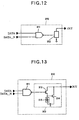
- FIGs. 2 and 3 show the logical structure and circuit configuration of one of the n single-bit comparators 100. All of the single-bit comparators 100 have this structure and configuration.
- a single-bit comparator 100 has three input terminals, denoted DATA, DATA_N, and ADDR, each of which receives one bit of the corresponding n-bit input signal.
- the received bits will be referred to as DATA, DATA_N, and ADDR below.
- the three input terminals are coupled to a two-input exclusive OR gate 101, which takes the exclusive logical OR of the DATA and ADDR bits.
- the output of the exclusive OR gate 101 drives a discharging element 102, which is coupled to a ground terminal and to an output terminal denoted OUT.
- the exclusive OR gate 101 has an inverter 103, which is coupled to the ADDR input terminal and generates a complementary signal denoted ADDR_N.
- This signal ADDR_N is supplied to the gate electrode of a PMOS transistor 104 and an n-channel metal-oxide-semiconductor field-effect transistor (hereinafter, NMOS transistor) 10B.
- the DATA signal is supplied to the gate electrodes of a PMOS transistor 105 and an NMOS transistor 108.
- ADDR is supplied to the gate electrodes of a PMOS transistor 106 and an NMOS transistor 109.
- DATA_N is supplied to the gate electrodes of a PMOS transistor 107 and an NMOS transistor 10A.
- the source electrodes of PMOS transistors 104 and 106 receive the power-supply potential, and their drain electrodes are coupled to the source electrodes of PMOS transistors 105 and 107, respectively.
- the source electrodes of NMOS transistors 109 and 10B receive the ground potential, and their drain electrodes are coupled to the source electrodes of NMOS transistors 108 and 10A, respectively.
- the drain electrodes of PMOS transistors 105 and 107 and NMOS transistors 108 and 10A are coupled in common to the gate electrode of an NMOS transistor 10C, which constitutes the discharging element 102.
- the source electrode of NMOS transistor 10C receives the ground potential, and its drain electrode is coupled to the output terminal OUT.
- Each single-bit comparator 100 thus has an NMOS open-drain output structure. More specifically, each single-bit comparator 100 outputs a single-bit result signal that is either pulled down to the low (ground) level or left in the high-impedance state, depending on the logic levels of ADDR, DATA, and DATA_N. These single-bit result signals merge into a combined result signal at the COMP node. The combined result signal is pulled down to the low level when any one of the single-bit result signals is pulled down to the low level.
- the output control circuit 110 has two input terminals, denoted DATA and DATA_N, that receive, for example, DATA ⁇ n> and DATA_N ⁇ n>. These input terminals are coupled to a two-input NAND gate 111, the output of which controls a discharging element 112.
- the discharging element 112 is coupled to a ground terminal and to another output terminal denoted OUT, distinct from the output terminals (also denoted OUT) of the single-bit comparators 100.
- the NAND gate 111 comprises PMOS transistors 113 and 114 and NMOS transistors 115 and 116.
- the DATA input terminal is coupled to the gate electrodes of PMOS transistor 113 and NMOS transistor 115.
- the DATA_N input terminal is coupled to the gate electrodes of PMOS transistor 114 and NMOS transistor 116.
- the source electrodes of PMOS transistors 113 and 114 receive the power-supply potential.
- the source electrode of NMOS transistor 116 receives the ground potential, and its drain electrode is coupled to the source electrode of NMOS transistor 115.
- the drain electrodes of PMOS transistors 113 and 114 and NMOS transistor 115 are coupled to the gate electrode of an NMOS transistor 117, which constitutes the discharging element 112.
- the source electrode of NMOS transistor 117 receives the ground potential, and its drain electrode is coupled to the output terminal OUT.
- the output control circuit 110 thus also has an NMOS open-drain output structure. More specifically, the output control circuit 110 outputs a ready signal that is either pulled down to the low level or left in the high-impedance state, depending on the logic levels of DATA and DATA_N.
- the output circuit 120 comprises an inverter 121 and a two-input NOR gate 122.
- the inverter 121 inverts the logic level of the COMP node, and supplies the inverted logic level to the NOR gate 122.
- the other input to the NOR gate 122 is taken from the READY node.
- the output of to the NOR gate 122 is the output signal HIT.
- FIG. 6 shows how the n-bit comparator 10 can be coupled to the tag control section of a cache memory.
- the tag control section has a number of rows of memory cells which store address information identifying data present in the cache.
- FIG. 6 shows only one row of memory cells 210, collectively storing one address. Each row of memory cells is controlled by a word line (WL).
- the outputs of the memory cells are amplified by a row of sense amplifiers 220, which are controlled by the clock signal CLK.
- Each sense amplifier 220 amplifies one address bit.
- the sense amplifiers 220 generate the signals DATA ⁇ 1:n> and DATA_N ⁇ 1:n> supplied to the n-bit comparator 10. DATA ⁇ 1:n> and DATA_N ⁇ 1:n> accordingly represent address data.
- NMOS transistors 108 and 109 or the path through NMOS transistors 10A and 10B is in the conducting state, depending on whether ADDR or ADDR_N is at the high level, while PMOS transistors 105 and 107 are both turned off.
- the gate electrode of NMOS transistor 10C is therefore at the ground level, and NMOS transistor 10C is turned off. Consequently, the output terminals of all of the single-bit comparators 100 are disconnected from the ground potential, and their single-bit result signals are in the high-impedance state.
- DATA and DATA_N are both high, so PMOS transistors 113 and 114 are both in the off-state, NMOS transistors 115 and 116 are both turned on, the gate electrode of NMOS transistor 117 is at the ground level, and NMOS transistor 117 is turned off.
- the output terminal of the output control circuit 110 is also disconnected from the ground potential, and the ready signal is also in the high-impedance state.
- the pre-charging of the COMP and READY nodes entails the pre-charging of the parasitic capacitance of the signal lines connected to these nodes, and the pre-charging of the parasitic capacitance of pn junctions in the single-bit comparators 100 and output control circuit 110, as well as the charging of the input capacitances of the inverter 121 and NOR gate 122.
- the ADDR ⁇ 1:n> input signal becomes valid, as indicated by the change from black to white in FIGs. 7 and 8.
- the ADDR ⁇ 1:n> input signal now represents an address to be compared with the address held in the row of memory cells 210 in FIG. 6.
- the subsequent operation differs depending on whether ADDR ⁇ 1:n> matches DATA ⁇ 1:n>, indicating a cache hit, or does not match DATA ⁇ 1:n>, indicating a cache miss.
- FIG. 7 illustrates a cache hit. Since every bit of ADDR ⁇ 1:n> matches every bit of DATA ⁇ 1:n>, in every single-bit comparator 100, the paths through PMOS transistors 104, 105, 106, and 107 in FIG. 3 are both in the non-conducting state, while either the path through NMOS transistors 108 and 109 or the path through NMOS transistors 10A or 10B is in the conducting state. The gate potential of NMOS transistor 10C therefore remains low, NMOS transistor 10C remains turned off, all of the single-bit result signals remain in the high-impedance state, and the COMP node remains charged at the high logic level.
- the NAND 111 gate in FIG. 5 receives complementary inputs. Since one input is low, the output of the NAND gate 111 goes high, turning on NMOS transistor 117, pulling down the ready signal, and forcing the READY node to discharge to ground.
- the NOR gate 122 now receives two low inputs: the high level of the COMP node inverted by inverter 121, and the low level of the READY node.
- the HIT signal output by the NOR gate 122 accordingly goes high, as shown in FIG. 7, indicating a cache hit.
- FIG. 8 illustrates a cache miss.
- at least one bit of ADDR ⁇ 1:n> fails to match the corresponding bit of DATA ⁇ 1:n>.
- the paths through NMOS transistors 108, 109, 10A, and 10B in FIG. 3 are both in the non-conducting state, and either the path through PMOS transistors 104 and 105 or the path through PMOS transistors 106 and 107 is in the conducting state, so the gate electrode of NMOS transistor 10C is brought to the high level and NMOS transistor 10C turns on, pulling down the corresponding single-bit result signal and forcing the COMP node to discharge to ground, as indicated in FIG. 8.
- the READY node also discharges to ground through the output control circuit 110, as it did in the case of a cache hit.
- the NOR gate 122 continues to receive one high input, the high input now coming from the inverter 121, which inverts the low level of the COMP node, so the HIT output signal remains at the low level.
- the READY node does not go low until the input signals DATA ⁇ 1:n> and DATA_N ⁇ 1:n> become valid, at which time ADDR ⁇ 1:n> is already valid.
- the HIT output signal is therefore held in the low state until all input signals have become valid, regardless of the length of the delay from the rise of the clock signal CLK to the falling transitions that mark the validity of DATA ⁇ 1:n> and DATA_N ⁇ 1:n>.
- the n-bit comparator 10 cannot output a false cache hit signal due to an accidental coincidence between DATA ⁇ 1:n> and ADDR ⁇ 1:n> during the period while any of the input signals are invalid.
- Timing design is also simplified in the circuits that use the HIT output signal, because the rise of the HIT output signal in a cache hit always occurs at the same time, as reliably determined by the fall of the ready signal.
- the timing of the HIT output signal does not depend on the number of mis-matching bits in a cache miss, because the HIT output signal remains constant in a cache miss.
- the n-bit comparator 10 of the first embodiment uses a NOR gate to produce the final output signal, but this NOR gate 122 has only two inputs.
- the second embodiment is an n-bit comparator 20 comprising n single-bit comparators 300, an output control circuit 310, an output circuit 320, and PMOS transistors 330 and 331.
- the structure of this n-bit comparator 20 is identical to the structure of the n-bit comparator 10 of the first embodiment, except for the internal structure of the single-bit comparators 300 and output control circuit 310.
- the single-bit comparators 300 have the same logical structure as in the first embodiment, comprising an exclusive OR gate 301 and a discharging element 302.
- the exclusive OR gate 301 is identical to the exclusive OR gate 101 in the first embodiment, having the circuit configuration shown in FIG. 3.
- the discharging element 302 comprises an NMOS transistor 303, a bipolar transistor 304, and a resistive element 305.
- the gate electrode of NMOS transistor 303 receives the output of the exclusive OR gate 301.
- the drain electrode of NMOS transistor 303 is coupled to the collector electrode of bipolar transistor 304, and to the output terminal OUT.
- the source electrode of NMOS transistor 303 is coupled to the base electrode of bipolar transistor 304, and to one terminal of the resistive element 305.
- the emitter electrode of bipolar transistor 304 and the other terminal of the resistive element 305 receive the ground potential.
- the output control circuit 310 has the same logical structure as in the first embodiment, comprising a NAND gate 311 and a discharging element 312.
- the NAND gate 311 is identical to the NAND gate 111 in the first embodiment, having the circuit configuration shown in FIG. 5.
- the discharging element 312 comprises an NMOS transistor 313, a bipolar transistor 314, and a resistive element 315.
- the gate electrode of NMOS transistor 313 receives the output of the NAND gate 311.
- the drain electrode of NMOS transistor 313 is coupled to the collector electrode of bipolar transistor 314, and to the output terminal OUT.
- the source electrode of NMOS transistor 313 is coupled to the base electrode of bipolar transistor 314, and to one terminal of the resistive element 315.
- the emitter electrode of bipolar transistor 314 and the other terminal of the resistive element 315 receive the ground potential.
- the single-bit comparators 300 and output control circuit 310 accordingly both have an open-collector output structure.
- the bipolar transistors 304 and 314 have a greater current-driving capability than the NMOS transistors 303 and 313, and a greater current-driving capability than the NMOS transistors 10C and 117 in the first embodiment.
- the resistive elements 302 and 312 are, for example, NMOS or PMOS transistors that are held in the on-state and have suitable on-resistance values.
- the overall circuit operation of the n-bit comparator 20 is similar to the operation of the n-bit comparator 10 in the first embodiment for both the cache hit and cache miss cases.
- the following description will focus on the operation of the single-bit comparators 300 and output control circuit 310 shown in FIGs. 11 and 13.
- ADDR ⁇ 1:n> matches DATA ⁇ 1:n> in every bit, then in every single-bit comparator 300, the output of the exclusive OR gate 301 in FIG. 11 remains low, NMOS transistor 303 remains in the off-state, bipolar transistor 304 also remains in the off-state, and the COMP node remains at the high level, permitting the HIT output signal to go high as in the first embodiment. If ADDR ⁇ 1:n> and DATA ⁇ 1:n> do not match, however, then in at least one single-bit comparator 300, the output of exclusive OR gate 301 goes high, NMOS transistor 303 turns on, bipolar transistor 304 turns on, the COMP node discharges quickly through bipolar transistor 304, and the HIT output signal is held at the low level.
- the second embodiment can operate at even higher speeds than the first embodiment, because the greater current-driving capability of the bipolar transistors 304 and 314 enables the COMP and READY nodes to discharge faster than in the first embodiment.
- the second embodiment permits a larger number of input bits, because the bipolar transistors 304 can more quickly discharge the additional parasitic capacitance of the COMP node that results from the increased number of single-bit comparators 300.
- the third embodiment is an n-bit comparator 30 comprising n single-bit comparators 400, an output control circuit 410, an output circuit 420, and PMOS transistors 430 and 431.
- the structure of this n-bit comparator 40 is identical to the structure of the n-bit comparator 10 of the first embodiment, except for the internal structure of the output control circuit 410.
- the output control circuit 410 is now similar in design to the single-bit comparators 400.
- FIG. 15 shows the logical structure of the single-bit comparators 400, each of which comprises an exclusive OR gate 401 and discharging element 402.
- FIG. 16 shows the circuit configuration of the exclusive OR gate 401, which is identical to the exclusive OR gate 101 in the first embodiment, shown in FIG. 3.
- the discharging element 402 is also identical to the discharging element 102 in the first embodiment.
- the output control circuit 410 has the same logical structure as in the first embodiment, comprising a NAND gate 411 coupled to the DATA and DATA_N input terminals, and a discharging element 412 that receives the output of the NAND gate 411 and drives the output terminal OUT.
- the discharging element 412 is identical to the discharging element 112 in the first embodiment, shown in FIGs. 4 and 5.
- the NAND gate 411 in the output control circuit 410 comprises PMOS transistors 413, 414, 415, 416 and NMOS transistors 417, 418, 419, and 41A, which are interconnected in the same way as the PMOS transistors 404, 405, 406, 407 and NMOS transistors 408, 409, 40A, and 40B in the exclusive OR gates 401 in the single-bit comparators 300, shown in FIG. 16.
- the same layout of circuit elements is used in both the NAND gate 411 and exclusive OR gates 401, comprising two pairs of PMOS transistors and two pairs of NMOS transistors, each pair of transistors coupled in series to a common output terminal, the two pairs of PMOS transistors being coupled in parallel with one another between the output terminal and the power supply, and the two pairs of NMOS transistors being coupled in parallel with one another between the output terminal and ground.
- the output terminal is the drain terminal 40C of transistors 405, 407, 408, and 40A.
- the output terminal is the drain terminal 41B of transistors 414, 416, 417, and 419.
- the DATA input terminal of the NAND gate 411 is coupled to the gate electrodes of PMOS transistors 413 and 414 and NMOS transistors 417 and 419.
- the DATA_N input terminal is coupled to the gate electrodes of PMOS transistors 415 and 416 and NMOS transistors 418 and 41A. These input connections differ from the input connections of the exclusive OR gates 401. It can be readily verified that the circuit configuration of the NAND gate 411 in FIG. 18 performs the logical NAND operation, supplying to the discharging element 412 a signal that is low when both inputs DATA and DATA_N are high, and is high when either DATA or DATA_N is low.
- the overall circuit operation of the n-bit comparator 30 is similar to the operation of the n-bit comparator 10 in the first embodiment for both the cache hit and cache miss cases. The following description will focus on the operation of the output control circuit 410 shown in FIGs. 17 and 18.
- a feature of the third embodiment is that the propagation delay of the DATA and DATA_N signals in the NAND gate 411 is equal to the propagation delay in the exclusive OR gates 401 in the single-bit comparators 400, because both have the same circuit configuration.
- the discharging elements 402 in the single-bit comparators 400 of the mis-matching bits therefore turn on at the same time as the discharging element 412 in the output control circuit 410. Timing differences between the two inputs to the NOR gate 422 in the output circuit 420 are thereby reduced, and the timing design of the n-bit comparator 30 as a whole is simplified.
- the circuit design process is also simplified, because the same layout can be employed in both the single-bit comparators 400 and output control circuit 410. Moreover, the process of design verification through computer simulation is simplified, because the single-bit comparators 400 and output control circuit 410 have the same parasitic capacitances and resistances and other parameters. Design turnaround time can therefore be shortened.
- the propagation delay of the ADDR signal in the inverter 403 in FIG. 16 can be ignored, because ADDR ⁇ 1:n> becomes valid before DATA ⁇ 1:N> and DATA_N ⁇ 1:n>.
- the discharging elements 402 and 412 in the single-bit comparators 400 and output control circuit 410 can be given the same structure as in the second embodiment, using bipolar transistors to achieve higher-speed operation or handle a larger number of bits.
- the fourth embodiment is an n-bit comparator 40 comprising n single-bit comparators 500, an output control circuit 510, an output circuit 520, PMOS transistors 530 and 531, and a capacitive dummy load 540.
- the fourth embodiment thus adds a dummy load 540 to the structure of the first embodiment.
- the other circuit elements in the fourth embodiment are identical to the corresponding elements in the first embodiment.
- the dummy load 540 is coupled to the READY node.
- the function of the dummy load 540 is to make the discharge time of the READY node equal to or greater than the discharge time of the COMP node, in the worst case in which there is only one non-matching bit and the COMP node discharges through just one single-bit comparator 500.
- the dummy load 540 comprises, for example, an NMOS transistor 541 having grounded gate and source electrodes, the drain electrode being coupled to the READY node. Since its gate electrode is grounded, NMOS transistor 541 is permanently turned off.
- the dimensions of the NMOS transistor 541 in the dummy load 540 should be adjusted so that the total parasitic capacitance of the READY node is equal to or greater than the total parasitic capacitance of the COMP node.
- the parasitic capacitance of the READY node includes both the parasitic capacitance of the interconnecting lines coupled to the READY node, and the parasitic junction capacitance in the coupled transistor or transistors in the discharging element 512 in the output control circuit 510.
- the parasitic capacitance of the COMP node includes the parasitic capacitance of the interconnecting lines coupling the COMP node to all n single-bit comparators 500, and the sum of the parasitic junction capacitances of transistors in the n discharging elements 502.
- the overall circuit operation of the n-bit comparator 40 is similar to the operation of the n-bit comparator 10 in the first embodiment for both the cache hit and cache miss cases, but the fourth embodiment provides superior protection against hazards in the HIT output signal when a cache miss occurs.
- FIG. 20 shows how such a hazard might occur in a cache miss in the first embodiment.
- the clock signal CLK goes high, the word line WL goes high, the input signals DATA ⁇ 1:n> and DATA_N ⁇ 1:n> go to complementary states, and the READY node goes low with the same timing as shown in FIG. 8. If the COMP node takes significantly longer than the READY node to discharge, there will be a delay before the COMP node goes low. During the interval between the fall of the READY potential and the fall of the COMP potential, the NOR gate 522 receives two low inputs, and the HIT output signal goes high, as shown, incorrectly indicating a cache hit.
- the READY node when a single bit mis-matches, the READY node does not discharge before the COMP node, because it has equal or greater parasitic capacitance. Hazards of the type shown in FIG. 20 accordingly do not occur.
- the COMP node discharges faster than the READY node, because the COMP node discharges through two or more discharging elements 502 while the READY node discharges through only a single discharging element 512.
- the capacitance of the dummy load 540 should be adjusted accordingly, to make the discharge time of the READY node equal to or greater than the worst-case discharge time of the COMP node.
- the fifth embodiment is an n-bit comparator 50 comprising n single-bit comparators 600, an output control circuit 610, an output circuit 620, PMOS transistors 630 and 631, and a dummy load 640. Except for the dummy load 640, these elements are similar to the corresponding elements in the fourth embodiment.
- the fourth embodiment allowed the single-bit comparators and output control circuit to use discharging elements with different current-driving capabilities.
- the fifth embodiment employs identical discharging elements 641, with equal current-driving capabilities, in both the single-bit comparators 600 and the output control circuit 610.
- the dummy load 640 comprises n - 1 more of these identical discharging elements 641 coupled in parallel to the READY terminal.
- the structure of the discharging elements 641 in the single-bit comparators 600, output control circuit 610, and dummy load 640 may be that shown in the first embodiment, comprising a single NMOS transistor.
- the discharging elements 641 may all have the structure shown in the second embodiment, each comprising an NMOS transistor, a bipolar transistor, and a resistive element, or any other suitable structure.
- the discharging elements 641 in the dummy load 640 are permanently turned off, e.g. by grounding the gate electrodes of their constituent NMOS transistors, so they do not pull down the potential of the READY terminal.
- the only function of the discharging elements 641 in the dummy load 640 is to provide additional parasitic junction capacitance for the READY node.
- the COMP node is coupled to n discharging elements 641 in the n single-bit comparators 600.
- the READY node is likewise coupled to n discharging elements 641 (one in the output control circuit 610 and n - 1 in the dummy load 640), so the parasitic junction capacitances of the COMP and READ nodes are exactly equal.
- the n-bit comparator 50 of the fifth embodiment operates in the same way as the n-bit comparator 40 of the fourth embodiment.
- the COMP and READY nodes discharge in substantially equal times, because both nodes are coupled to identical parasitic junction capacitances, and both nodes discharge through identical discharging elements 641. If more than one bit mis-matches, the COMP node discharges more rapidly than the READY node. In either case, no hazards appear in the HIT output signal.
- the advantage of the fifth embodiment is that the use of structurally identical discharging elements 641 assures equal junction capacitances and equal current-driving capabilities, without the need to rely on calculated values for these parameters.
- the circuit design process is therefore simplified, and timing reliability is improved. In particular, fabrication process variations that alter the characteristics of the discharging elements do not upset the circuit timing relationships.
- the n-bit comparator 60 of the sixth embodiment comprises n single-bit comparators 700, an output control circuit 710, an output circuit 720, PMOS transistors 730 and 731, and a dummy load 740. These elements are identical to the corresponding elements in the fourth embodiment.
- the difference between the n-bit comparator 40 of the fourth embodiment and the n-bit comparator 60 of the sixth embodiment concerns the physical layout and input connections of the circuit elements, specifically, the disposition and input connections of the output control circuit 710.
- the input signal lines to the output control circuit 710 are branched from the input signal lines of one of the single-bit comparators 700.
- This single-bit comparator 700 is the single-bit comparator 700 which is disposed farthest from the output circuit 720 in terms of interconnecting signal-line length.
- the output control circuit 710 is placed physically adjacent to this single-bit comparator 700, so that both branches of the input signal lines have substantially the same length and substantially equal parasitic resistance and capacitance. Similarly, the length of the signal line interconnecting this farthest single-bit comparator 700 to the output circuit 720, passing through the COMP node, is substantially equal to the length of the signal line interconnecting the output control circuit 710 to the output circuit 720, passing through the READY node, and both signal lines have substantially equal parasitic resistances and capacitances.
- the single-bit comparator 700 that receives the first bits DATA ⁇ 1>, DATA_N ⁇ 1>, and ADDR ⁇ 1> of the input signals is separated from the output circuit 720 by the greatest length of interconnecting signal line, then the first-bit input signal lines are branched to bring DATA ⁇ 1> and DATA_N ⁇ 1> to both this farthest single-bit comparator 700 and the output control circuit 710, as shown in FIG. 22. It may appear that the single-bit comparator 700 receiving input signals DATA ⁇ 1>, DATA_N ⁇ 1>, and ADDR ⁇ 1> is closest to the output circuit 720, rather than farthest away, but FIG. 22 is a schematic diagram, and does not depict the actual physical layout relationships of the circuit elements.
- the overall circuit operation of the n-bit comparator 60 in the sixth embodiment is similar to the operation of the n-bit comparator 40 in the fourth embodiment for both the cache hit and cache miss cases.
- the discharging element 702 in the single-bit comparator 700 that receives this bit and the discharging element 712 in the output control circuit 710 turn on at the substantially same time, because the input signals DATA ⁇ 1> and DATA_N ⁇ 1> arrive at both this single-bit comparator 700 and the output control circuit 710 at the same time. Since the dummy load 740 makes the discharge time of the READY node equal to or greater than the discharge time of the COMP node, the input to the output circuit 720 from the READY node does not change before the input from the COMP node, producing a hazard-free HIT output signal.
- the output circuit 720 receives a low input from the COMP node before receiving a low input from the READY node, assuring that the HIT output signal stays low and again avoiding hazards.
- the sixth embodiment helps to ensure that the READY input to the output circuit 720 does not fall before the COMP input, no matter how many input bits there are, and no matter how far the farthest single-bit comparator 700 is from the output circuit 720.
- the seventh embodiment is an n-bit comparator 70 comprising n single-bit comparators 800, an output control circuit 810, an output circuit 820, PMOS transistors 830 and 831, and a dummy load 840.
- the seventh embodiment is identical to the fifth embodiment, except for the internal structure of the dummy load 840.
- the n-bit comparator 70 of the seventh embodiment uses identical discharging elements 841 in the single-bit comparators 800, the output control circuit 810, and the dummy load 840. Differing from the fifth embodiment, the seventh embodiment places at least n of these discharging elements 841 in the dummy load 840, making the parasitic junction capacitance of the READY node greater than the parasitic junction capacitance of the COMP node.
- the overall circuit operation of the n-bit comparator 70 of the seventh embodiment is similar to the operation of the fifth embodiment for both the cache hit and cache miss cases, except that when a cache miss occurs, even if only one bit mis-matches, the potential of the READY node falls more slowly than the potential of the COMP node. This is because the parasitic junction capacitance that must be discharged at the READY node exceeds the parasitic junction capacitance that must be discharged at the COMP node.
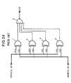
- FIG. 24 shows an example of a classic n-bit comparator when n is equal to four.
- the individual bits of input signals DATA ⁇ 1:4> and ADDR ⁇ 1:4> are supplied to four exclusive OR gates 1, 2, 3, and 4, the outputs of which are combined by a four-input NOR gate 5.
- the circuit in FIG. 24 requires a separate interconnecting line to the NOR gate 5 from each of the exclusive OR gates 1, 2, 3, and 4, which correspond to the single-bit comparators of the present invention.
- the present invention saves space by using a single interconnecting line for all of the single-bit comparators.
- the embodiments above have been described in relation to hit-miss detection in a cache memory, but the invention is not restricted to this application.
- the invented multiple-bit comparator can be applied in any circuit that must compare two multiple-bit input signals A and B and generate an output signal indicating whether the two input signals are identical or not, provided the following two conditions are satisfied.
- the first condition is that one of the input signals, e.g. signal B, must have valid and invalid states which can be detected from transitions in the signal itself.
- this condition was satisfied by having signal B input as a pair of signals DATA ⁇ 1:n> and DATA_N ⁇ 1:n> which were complementary when valid and identical when invalid.
- the second condition is that this signal B must not change from the invalid state to the valid state until the other input signal (signal A) becomes valid.
- the invented comparator could be described as deciding whether all bits of two input signals (ADDR ⁇ 1:n> and DATA_N ⁇ 1:n>) mis-match, instead of whether all bits of two input signals (ADDR ⁇ 1:n> and DATA ⁇ 1:n>) match.
- the internal circuit configurations of the single-bit comparators, output control circuit, and output circuit are not limited to the configurations described in the embodiments above. These circuits may have other configurations, employing different numbers or types of circuit elements, and different interconnection relationships.
Landscapes
- Engineering & Computer Science (AREA)
- Theoretical Computer Science (AREA)
- General Physics & Mathematics (AREA)
- Physics & Mathematics (AREA)
- Mathematical Analysis (AREA)
- Pure & Applied Mathematics (AREA)
- Mathematical Optimization (AREA)
- General Engineering & Computer Science (AREA)
- Computational Mathematics (AREA)
- Logic Circuits (AREA)
- Dram (AREA)
- Synchronisation In Digital Transmission Systems (AREA)
- Analogue/Digital Conversion (AREA)
Claims (28)
- Multibit-Vergleicher, der ein erstes Signal und ein Paar von zweiten Signalen empfängt, wobei das erste Signal und das Paar der zweiten Signale Multibit-Signale sind, wobei das Paar der zweiten Signale in einem ungültigen Zustand verbleibt, in dem wenigstens ein entsprechendes Paar von Bits in dem Paar der zweiten Signale sich auf identischen logischen Niveaus befinden, bis das erste Signal gültig wird, und wobei es sich dann in einem gültigen Zustand ändert, in dem alle entsprechenden Paare von Bits in dem Paar der zweiten Signale auf komplementären logischen Niveaus sind, um ein Ausgangssignal zu erzeugen, welches anzeigt, ob alle Bits des ersten Signals mit allen Bits eines speziellen Signals in dem Paar der zweiten Signale übereinstimmen, der eine Vielzahl von Einzelbit-Vergleichem (100) hat, um individuelle Bits in dem ersten Signal mit individuellen Bits des Paares der zweiten Signale zu vergleichen und entsprechende Einzelbit-Resultat-Signale zu erzeugen, und der einen ersten Noden hat, die mit der Vielzahl von Einzelbit-Verglichern (100) gekoppelt ist und die Einzelbit-Restultat-Signale empfängt, um die Einzelbit-Resultat-Signale mit einem kombinierten Resultat-Signal zu kombinieren, gekennzeichnet durch
eine Ausgangssteuerschaltung (110), um eines des entsprechenden Paares der Bits in dem Paar der zweiten Signale zu vergleichen, Übergänge derselben zu detektieren und ein Bereit-Signal auszugeben, welches anzeigt, wenn das Paar der zweiten Signale gültig ist;
einen zweiten Noden, der mit der Ausgangssteuerschaltung (110) gekoppelt ist, um das Bereit-Signal zu empfangen; und
eine Ausgangsschaltung (120), die mit dem ersten Noden und dem zweiten Noden gekoppelt ist, um eine logische Operation an dem kombinierten Resultat-Signal und dem Bereit-Signal durchzuführen, um dadurch das Ausgangssignal zu erzeugen, wobei das Ausgangssignal in einem festen Zustand gehalten wird, während das Bereit-Signal anzeigt, dass das Paar der zweiten Signale gültig ist, und wobei sich das Ausgangssignal in Antwort auf das kombinierte Resultat-Signal ändert, wenn das Bereit-Signal anzeigt, dass das Paar der zweiten Signale gültig ist. - Vergleicher nach Anspruch 1, worin die Vielzahl der Einzelbit-Vergleicher (100) mit dem ersten Noden in einer verdrahteten ODER-Konfiguration gekoppelt sind.
- Vergleicher nach Anspruch 2, ferner umfassend ein erstes Voraufladeelement (130) zum Voraufladen des ersten Noden mit einem ersten logischen Niveau, während das Paar der zweiten Signale gültig ist.
- Vergleicher nach Anspruch 3, worin jeder der Einzelbit-Vergleicher (100) separat ein erstes Entladeelement (102) aufweist, um den ersten Noden von dem ersten logischen Niveau auf ein zweites logisches Niveau in Antwort auf das erste Signal und das Paar der zweiten Signale zu entladen, wenn das Paar der zweiten Signale gültig ist.
- Vergleicher nach Anspruch 4, worin das erste Entladeelement (302) einen Feldeffekttransistor (10C) aufweist, der eine Drain-Elektrode hatte, die mit dem ersten Noden gekoppelt ist, wobei den Einzelbit-Vergleichern (100) eine Ausgangsstruktur mit offenem Drain gegeben wird.
- Vergleicher nach Anspruch 4, worin das erste Entladeelement (302) einen bipolaren Transistor (304) aufweist, der eine Kollektorelektrode hat, die mit dem ersten Noden gekoppelt ist, wobei den Einzelbit-Vergleichern (300) eine Ausgangsstruktur mit offenem Kollektor gegeben wird.
- Vergleicher nach Anspruch 4, ferner umfassend ein zweites Voraufladeelement (131) zum Voraufladen des zweiten Noden auf ein drittes logisches Niveau, während das Paar der zweiten Signale ungültig ist.
- Vergleicher nach Anspruch 7, worin das erste logische Niveau und das dritte logische Niveau identisch sind.
- Vergleicher nach Anspruch 7, worin das erste logische Niveau und das dritte logische Niveau unterschiedlich sind.
- Vergleicher nach Anspruch 7, worin die Ausgangssteuerschaltung (110) ein zweites Entladeelement (112) aufweist, um den zweiten Noden von dem dritten logischen Niveau auf ein viertes logisches Niveau zu entladen, wenn das Paar der zweiten Signale gültig ist.
- Vergleicher nach Anspruch 10, worin das zweiten Entladeelement (112) einen Feldeffekttransistor (117) aufweist, der eine Drainelektrode hat, die mit dem zweiten Noden gekoppelt ist, wobei der Ausgangssteuerschaltung (110) eine Ausgangsstruktur mit offenem Drain gegeben wird.
- Vergleicher nach Anspruch 10, worin das zweite Entladeelement (312) einen bipolaren Transistor (314) aufweist, der eine Kollektorelektrode hat, die mit dem zweiten Noden gekoppelt ist, wobei der Ausgangssteuerschaltung (310) eine Ausgangsstruktur mit offenem Kollektor gegeben wird.
- Vergleicher nach Anspruch 10, worin jeder der Einzelbit-Vergleicher (100) separat ein erstes logisches Gatter (101) hat, das ein Bit des ersten Signals und ein entsprechendes Paar von Bits von dem Paar der zweiten Signale empfängt, um das erste Entladeelement (102) zu steuern.
- Vergleicher nach Anspruch 13, worin die Ausgangssteuerschaltung (110) ein zweites logisches Gatter (111) hat, das ein entsprechendes Paar von Bits in dem Paar der zweiten Signale empfängt, um das zweite Entladeelement (112) zu steuern.
- Vergleicher nach Anspruch 14, worin das zweite logische Gatter (411) und das erste logische Gatter (401) identische Schaltungsauslegungen mit unterschiedlichen Eingangssignalen aufweisen.
- Vergleicher nach Anspruch 15, worin das zweite logische Gatter (411) und die ersten logischen Gatter (401) jeweils separat umfassen:einen Ausgangsanschluß (40C);ein erstes Paar von p-Kanal-Feldeffekttransestoren (404, 405), die in Reihe mit dem Ausgangssignal gekoppelt sind;ein zweites Paar von p-Kanal-Feldeffekttransestoren (406, 407), die in Reihe mit dem Ausgangsanschluß parallel mit dem ersten Paar der p-Kanal-Feldeffekttransestoren gekoppelt sind;ein erstes Paar von n-Kanal-Feldeffekttransestoren (408, 409), die in Reihe mit dem Ausgangsanschluß gekoppelt sind; undein zweites Paar von n-Kanal-Feldeffekttransestoren (40A, 40B), die in Reihe mit dem Ausgangsanschluß parallel mit dem ersten Paar der n-Kanal-Feldeffekttransestoren gekoppelt sind.
- Vergleicher nach Anspruch 1, ferner umfassend eine Blindlast (540), die mit dem zweiten Noden gekoppelt ist und das Bereit-Signal mit einer Signalverzögerung nicht weniger als eine Signalverzögerung des kombinierten Resultat-Signals liefert, wenn das erste Signal mit dem speziellen einen Signal in dem Paar der zweiten Signale in gerade einem Bit nicht übereinstimmt.
- Vergleicher nach Anspruch 10, worin die ersten Entladeelemente (641) in den Einzelbit-Vergleichern (600) strukturell identisch mit dem zweiten Entladeelement (641) in der Ausgangssteuerschaltung (610) sind, ferner umfassend:eine Blindlast (640), die mit dem zweiten Noden gekoppelt ist, wobei die Blindlast eine Anzahl von dritten Entladeelementen (641) hat, die ebenfalls strukturell identisch mit den zweiten Entladeelementen sind, wobei die dritten Entladeelemente permanent ausgeschaltet sind und den zweiten Noden nicht entladen.
- Vergleicher nach Anspruch 18, worin den zweiten die Zahl der dritten Entladeelemente (641) nicht geringer ist als die Zahl der Bits in dem ersten Signal.
- Vergleicher nach Anspruch 18, worin die Zahl der dritten Entladeelemente (841) nicht geringer ist als die Zahl der Bits in dem ersten Signal.
- Vergleicher nach Anspruch 1, worin die Ausgangssteuerschaltung (710) neben dem am weitesten entfernt liegenden der Einzelbit-Vergleicher (700) von der Ausgangsschaltung (720) liegt bezogen auf die Länge der Signalverbindungslinie, wobei die Ausgangssteuerschaltung und der am weitesten entfernt liegende der Einzelbit-Vergleicher beide ein identisches Paar von entsprechenden Bits in dem Paar der zweiten Signale empfangen.
- Verfahren zum Vergleichen eines ersten Signals (ADDR<1:n>) mit einem zweiten Signal (DATA<1:n>, DATA_N<1:n>), wobei das erste Signal und das zweite Signal Signale mit einer Vielzahl von Bits sind, um festzustellen, ob alle Bits des ersten Signals mit entsprechenden Bits des zweiten Signals übereinstimmen, wobei das zweite Signal Paare von Bits (DATA, DATA_N) umfasst, die komplementäre Werte haben, wenn das zweite Signal gültig ist, und identische Werte haben, wenn das zweite Signal ungültig ist, wobei das Verfahren den Vergleich individueller Bits (ADDR) des ersten Signals (ADDR<1:n>) mit entsprechenden Bits (DATA, DATA_N) des zweiten Signals (DATA<1:n>, DATA_N<1:n>) umfasst, um individuelle Vergleichsresultate (OUT in Figur 2) zu erzeugen, und gekennzeichnet durch die Schritte:Detektieren, wenn das zweite Signal (DATA<1:n>, DATA_N<1:n>) gültig ist und wenn das zweite Signal ungültig ist, indem eine logische Operation auf ein Paar von Bits (DA-TA<n>, DATA_N<n>) in dem zweiten Signal durchgeführt wird, um Übergänge in dem zweiten Signal zu detektieren;Halten eines Ausgangssignals (HIT) auf einem festen logischen Niveau, wenn das zweite Signal (DATA<1:n>, DATA_N<1:n>) ungültig ist; undSteuern des Ausgangssignals (HIT) in Antwort auf die individuellen Vergleichsresultate (OUT), wenn das zweite Signal gültig wird.
- Verfahren nach Anspruch 22, worin das erste logische Niveau ein logisches Niveau ist, welches anzeigt, dass das erste Signal nicht mit dem zweiten Signal übereinstimmt.
- Verfahren nach Anspruch 22, worin der Schritt des Steuerns die folgenden weiteren Schritte umfasst:Voraufladen eines ersten Noden (COMP) auf ein erstes logisches Niveau, während das zweite Signal (DATA<1:n>, DATA_N<1:n>) ungültig ist;Entladen des ersten Noden (COMP) auf ein zweites logisches Niveau, wenn eines der individuellen Vergleichsresultate (OUT) anzeigt, dass das erste Signal (ADDR<1:n>) nicht mit dem zweiten Signal (DATA<1:n>, DATA_N<1:n>) übereinstimmen.
- Verfahren nach Anspruch 24, worin der Schritt des Haltens die folgenden weiteren Schritte umfasst:Voraufladen eines zweiten Noden (READY) auf ein drittes logisches Niveau, während das zweite Signal (DATA<1:n>, DATA_N<1:n>) gültig ist; undEntladen des zweiten Noden (READY) auf ein viertes logisches Niveau, wenn das zweite Signal (DATA<1:n>, DATA_N<1:n>) gültig wird, wobei das Ausgangssignal (HIT) erzeugt wird, indem eine logische Operation auf die logischen Niveaus des ersten Noden (COMP) und des zweiten Noden (READY) ausgeführt wird.
- Verfahren nach Anspruch 25, umfassend den weiteren Schritt des Koppelns des zweiten Noden (READY) mit einer kapazitiven Blindlast (540), wodurch eine Entladezeit des zweiten Noden eingestellt wird.
- Verfahren nach Anspruch 26, worin die Entladezeit des zweiten Noden (READY) auf eine Zeit eingestellt wird, die gleich einer Entladezeit des ersten Noden (COMP) ist, wenn nur ein Bit des ersten Signals (ADDR<1:n>) nicht mit einem entsprechenden Bit in dem zweiten Signal (DATA<1:n>, DATA_N<1:n>) aus dem Text übereinstimmen.
- Verfahren nach Anspruch 27, worin die Entladezeit des zweiten Noden (READY) auf eine Zeit eingestellt wird, die größer ist als eine Entladezeit des ersten Noden (COMP), wenn nur ein Bit des ersten Signals (ADDR<1:n>) nicht mit einem entsprechenden Bit in dem zweiten Signal (DATA<1:n>, DATA_N<1:n>) übereinstimmen.
Applications Claiming Priority (3)
| Application Number | Priority Date | Filing Date | Title |
|---|---|---|---|
| JP10212996A JP3617569B2 (ja) | 1996-04-24 | 1996-04-24 | 多ビット一致回路 |
| JP102129/96 | 1996-04-24 | ||
| JP10212996 | 1996-04-24 |
Publications (3)
| Publication Number | Publication Date |
|---|---|
| EP0809178A2 EP0809178A2 (de) | 1997-11-26 |
| EP0809178A3 EP0809178A3 (de) | 1999-02-24 |
| EP0809178B1 true EP0809178B1 (de) | 2002-09-04 |
Family
ID=14319175
Family Applications (1)
| Application Number | Title | Priority Date | Filing Date |
|---|---|---|---|
| EP97104090A Expired - Lifetime EP0809178B1 (de) | 1996-04-24 | 1997-03-11 | Multibit-Vergleicher welcher feststellt, wann das Ausgangssignal sicher ist und ein verringertes Fehlerrisiko hat |
Country Status (7)
| Country | Link |
|---|---|
| US (1) | US5910762A (de) |
| EP (1) | EP0809178B1 (de) |
| JP (1) | JP3617569B2 (de) |
| KR (1) | KR100364311B1 (de) |
| CN (1) | CN1096635C (de) |
| DE (1) | DE69715088T2 (de) |
| TW (1) | TW413765B (de) |
Families Citing this family (6)
| Publication number | Priority date | Publication date | Assignee | Title |
|---|---|---|---|---|
| JP3490885B2 (ja) * | 1998-02-24 | 2004-01-26 | 三洋電機株式会社 | コンパレータ |
| US6456116B1 (en) * | 2001-04-11 | 2002-09-24 | Hewlett-Packard Company | Dynamic comparator circuit |
| US6765410B2 (en) | 2001-12-20 | 2004-07-20 | Sun Microsystems, Inc. | Method and apparatus for performing a hazard-free multi-bit comparison |
| KR100723484B1 (ko) * | 2005-02-07 | 2007-05-30 | 삼성전자주식회사 | 적은 면적과 향상된 동작속도를 갖는 비교기 |
| US12134713B2 (en) | 2018-12-28 | 2024-11-05 | Microchip Technology Incorporated | Classifying comparators based on comparator offsets |
| WO2020139451A1 (en) * | 2018-12-28 | 2020-07-02 | Microchip Technology Incorporated | Classifying comparators based on comparator offsets |
Family Cites Families (6)
| Publication number | Priority date | Publication date | Assignee | Title |
|---|---|---|---|---|
| JPS61252706A (ja) * | 1985-05-02 | 1986-11-10 | Hitachi Ltd | コンパレ−タ |
| NL8900549A (nl) * | 1989-03-07 | 1990-10-01 | Philips Nv | Vergelijkschakeling bevattende een maskeermechanisme voor transiente verschillen, vergelijkschakelingssysteem, en verwerkingsinrichting bevattende zulke vergelijkschakelingen. |
| US5218246A (en) * | 1990-09-14 | 1993-06-08 | Acer, Incorporated | MOS analog XOR amplifier |
| US5281946A (en) * | 1992-08-17 | 1994-01-25 | Motorola, Inc. | High-speed magnitude comparator circuit |
| JPH0675748A (ja) * | 1992-08-27 | 1994-03-18 | Matsushita Electric Ind Co Ltd | 1ビット比較器とこれを用いた多ビット比較器 |
| US5528181A (en) * | 1994-11-02 | 1996-06-18 | Advanced Micro Devices, Inc. | Hazard-free divider circuit |
-
1996
- 1996-04-24 JP JP10212996A patent/JP3617569B2/ja not_active Expired - Fee Related
-
1997
- 1997-03-11 DE DE69715088T patent/DE69715088T2/de not_active Expired - Lifetime
- 1997-03-11 EP EP97104090A patent/EP0809178B1/de not_active Expired - Lifetime
- 1997-03-20 US US08/822,340 patent/US5910762A/en not_active Expired - Fee Related
- 1997-03-24 TW TW086103720A patent/TW413765B/zh not_active IP Right Cessation
- 1997-04-24 CN CN97110393A patent/CN1096635C/zh not_active Expired - Fee Related
- 1997-04-24 KR KR1019970015420A patent/KR100364311B1/ko not_active Expired - Fee Related
Also Published As
| Publication number | Publication date |
|---|---|
| EP0809178A3 (de) | 1999-02-24 |
| EP0809178A2 (de) | 1997-11-26 |
| JPH09288562A (ja) | 1997-11-04 |
| JP3617569B2 (ja) | 2005-02-09 |
| CN1169562A (zh) | 1998-01-07 |
| TW413765B (en) | 2000-12-01 |
| US5910762A (en) | 1999-06-08 |
| DE69715088D1 (de) | 2002-10-10 |
| CN1096635C (zh) | 2002-12-18 |
| KR970071244A (ko) | 1997-11-07 |
| KR100364311B1 (ko) | 2002-12-18 |
| DE69715088T2 (de) | 2003-04-17 |
Similar Documents
| Publication | Publication Date | Title |
|---|---|---|
| JP3851224B2 (ja) | 内容アドレス・メモリ装置 | |
| US6829153B1 (en) | Content addressable memory (CAM) devices having CAM array blocks therein that perform pipelined and interleaved search, write and read operations and methods of operating same | |
| JP3095064B2 (ja) | 連想記憶装置 | |
| US6901020B2 (en) | Integrated charge sensing scheme for resistive memories | |
| CN100520969C (zh) | 减少内容可寻址存储器中的能量使用的电路和存储器 | |
| US6147891A (en) | Match line control circuit for content addressable memory | |
| EP0918335A2 (de) | Assoziativspeicher | |
| US20130182482A1 (en) | Content addressable memory device | |
| RU2414014C2 (ru) | Способ и устройство для уменьшения потребляемой мощности в ассоциативной памяти | |
| EP0809178B1 (de) | Multibit-Vergleicher welcher feststellt, wann das Ausgangssignal sicher ist und ein verringertes Fehlerrisiko hat | |
| US20010008493A1 (en) | Associative memory for accomplishing longest coincidence data detection by two comparing operations | |
| US9607668B2 (en) | Systems, circuits, and methods for charge sharing | |
| US5402379A (en) | Precharge device for an integrated circuit internal bus | |
| Hussain et al. | Efficient matchline controller for hybrid content addressable memory | |
| US9412425B2 (en) | Device and method for improving reading speed of memory | |
| US7391633B2 (en) | Accelerated searching for content-addressable memory | |
| EP0558733B1 (de) | Direktzugriffvergleichsmatrix | |
| US6721193B2 (en) | Cache memory | |
| EP1271548A1 (de) | Inhaltsadressierbarer Speicher mit AND Gatter Ubereinstimmungssignalkombinationsschaltung | |
| US6859376B2 (en) | Signal detection circuit for detecting multiple match in arranged signal lines | |
| US6813179B2 (en) | Cache memory | |
| US7408797B2 (en) | Methods and apparatus for content addressable memory arrays including shared match lines |
Legal Events
| Date | Code | Title | Description |
|---|---|---|---|
| PUAI | Public reference made under article 153(3) epc to a published international application that has entered the european phase |
Free format text: ORIGINAL CODE: 0009012 |
|
| AK | Designated contracting states |
Kind code of ref document: A2 Designated state(s): DE FR NL |
|
| PUAL | Search report despatched |
Free format text: ORIGINAL CODE: 0009013 |
|
| AK | Designated contracting states |
Kind code of ref document: A3 Designated state(s): DE FR NL |
|
| 17P | Request for examination filed |
Effective date: 19990414 |
|
| 17Q | First examination report despatched |
Effective date: 20010419 |
|
| GRAG | Despatch of communication of intention to grant |
Free format text: ORIGINAL CODE: EPIDOS AGRA |
|
| GRAG | Despatch of communication of intention to grant |
Free format text: ORIGINAL CODE: EPIDOS AGRA |
|
| GRAH | Despatch of communication of intention to grant a patent |
Free format text: ORIGINAL CODE: EPIDOS IGRA |
|
| GRAH | Despatch of communication of intention to grant a patent |
Free format text: ORIGINAL CODE: EPIDOS IGRA |
|
| GRAA | (expected) grant |
Free format text: ORIGINAL CODE: 0009210 |
|
| AK | Designated contracting states |
Kind code of ref document: B1 Designated state(s): DE FR NL |
|
| REF | Corresponds to: |
Ref document number: 69715088 Country of ref document: DE Date of ref document: 20021010 |
|
| ET | Fr: translation filed | ||
| PLBE | No opposition filed within time limit |
Free format text: ORIGINAL CODE: 0009261 |
|
| STAA | Information on the status of an ep patent application or granted ep patent |
Free format text: STATUS: NO OPPOSITION FILED WITHIN TIME LIMIT |
|
| 26N | No opposition filed |
Effective date: 20030605 |
|
| REG | Reference to a national code |
Ref country code: FR Ref legal event code: TP |
|
| PGFP | Annual fee paid to national office [announced via postgrant information from national office to epo] |
Ref country code: FR Payment date: 20100324 Year of fee payment: 14 |
|
| PGFP | Annual fee paid to national office [announced via postgrant information from national office to epo] |
Ref country code: NL Payment date: 20100316 Year of fee payment: 14 Ref country code: DE Payment date: 20100318 Year of fee payment: 14 |
|
| REG | Reference to a national code |
Ref country code: NL Ref legal event code: V1 Effective date: 20111001 |
|
| REG | Reference to a national code |
Ref country code: FR Ref legal event code: ST Effective date: 20111130 |
|
| PG25 | Lapsed in a contracting state [announced via postgrant information from national office to epo] |
Ref country code: NL Free format text: LAPSE BECAUSE OF NON-PAYMENT OF DUE FEES Effective date: 20111001 Ref country code: FR Free format text: LAPSE BECAUSE OF NON-PAYMENT OF DUE FEES Effective date: 20110331 Ref country code: DE Free format text: LAPSE BECAUSE OF NON-PAYMENT OF DUE FEES Effective date: 20111001 |
|
| REG | Reference to a national code |
Ref country code: DE Ref legal event code: R119 Ref document number: 69715088 Country of ref document: DE Effective date: 20111001 |