EP0808027A2 - Four-terminal power MOSFET switch having reduced threshold voltage and on-resistance - Google Patents
Four-terminal power MOSFET switch having reduced threshold voltage and on-resistance Download PDFInfo
- Publication number
- EP0808027A2 EP0808027A2 EP97107834A EP97107834A EP0808027A2 EP 0808027 A2 EP0808027 A2 EP 0808027A2 EP 97107834 A EP97107834 A EP 97107834A EP 97107834 A EP97107834 A EP 97107834A EP 0808027 A2 EP0808027 A2 EP 0808027A2
- Authority
- EP
- European Patent Office
- Prior art keywords
- mosfet
- voltage
- gate
- terminals
- terminal
- Prior art date
- Legal status (The legal status is an assumption and is not a legal conclusion. Google has not performed a legal analysis and makes no representation as to the accuracy of the status listed.)
- Granted
Links
- 230000002829 reductive effect Effects 0.000 title abstract description 8
- 238000000034 method Methods 0.000 claims description 16
- 239000008186 active pharmaceutical agent Substances 0.000 claims description 14
- 210000000746 body region Anatomy 0.000 claims description 14
- 239000004065 semiconductor Substances 0.000 claims description 8
- 239000000758 substrate Substances 0.000 claims description 5
- 230000001965 increasing effect Effects 0.000 description 29
- 238000010586 diagram Methods 0.000 description 19
- 239000007943 implant Substances 0.000 description 16
- 239000002019 doping agent Substances 0.000 description 13
- 230000007423 decrease Effects 0.000 description 12
- 230000000694 effects Effects 0.000 description 10
- 230000008901 benefit Effects 0.000 description 7
- 230000008569 process Effects 0.000 description 7
- 229920006395 saturated elastomer Polymers 0.000 description 6
- 230000000670 limiting effect Effects 0.000 description 5
- 238000004519 manufacturing process Methods 0.000 description 5
- 229910052710 silicon Inorganic materials 0.000 description 5
- 239000010703 silicon Substances 0.000 description 5
- XUIMIQQOPSSXEZ-UHFFFAOYSA-N Silicon Chemical compound [Si] XUIMIQQOPSSXEZ-UHFFFAOYSA-N 0.000 description 4
- 229910052751 metal Inorganic materials 0.000 description 4
- 239000002184 metal Substances 0.000 description 4
- 230000035945 sensitivity Effects 0.000 description 4
- 238000013459 approach Methods 0.000 description 3
- 230000015556 catabolic process Effects 0.000 description 3
- 230000006872 improvement Effects 0.000 description 3
- 230000000052 comparative effect Effects 0.000 description 2
- 230000001939 inductive effect Effects 0.000 description 2
- 239000000463 material Substances 0.000 description 2
- 238000012856 packing Methods 0.000 description 2
- 230000009467 reduction Effects 0.000 description 2
- 239000000243 solution Substances 0.000 description 2
- OAICVXFJPJFONN-UHFFFAOYSA-N Phosphorus Chemical compound [P] OAICVXFJPJFONN-UHFFFAOYSA-N 0.000 description 1
- 206010035148 Plague Diseases 0.000 description 1
- 241000607479 Yersinia pestis Species 0.000 description 1
- 230000002411 adverse Effects 0.000 description 1
- 230000003466 anti-cipated effect Effects 0.000 description 1
- 229910052785 arsenic Inorganic materials 0.000 description 1
- RQNWIZPPADIBDY-UHFFFAOYSA-N arsenic atom Chemical compound [As] RQNWIZPPADIBDY-UHFFFAOYSA-N 0.000 description 1
- 230000015572 biosynthetic process Effects 0.000 description 1
- 230000001413 cellular effect Effects 0.000 description 1
- 238000010276 construction Methods 0.000 description 1
- 230000007812 deficiency Effects 0.000 description 1
- 230000005669 field effect Effects 0.000 description 1
- 230000001771 impaired effect Effects 0.000 description 1
- 238000002347 injection Methods 0.000 description 1
- 239000007924 injection Substances 0.000 description 1
- 230000007246 mechanism Effects 0.000 description 1
- 238000005457 optimization Methods 0.000 description 1
- 230000036961 partial effect Effects 0.000 description 1
- 229910052698 phosphorus Inorganic materials 0.000 description 1
- 239000011574 phosphorus Substances 0.000 description 1
- 229920001690 polydopamine Polymers 0.000 description 1
- 230000002441 reversible effect Effects 0.000 description 1
- 238000004904 shortening Methods 0.000 description 1
- 238000003860 storage Methods 0.000 description 1
- 230000001360 synchronised effect Effects 0.000 description 1
- 238000005303 weighing Methods 0.000 description 1
Images


Classifications
-
- H—ELECTRICITY
- H01—ELECTRIC ELEMENTS
- H01L—SEMICONDUCTOR DEVICES NOT COVERED BY CLASS H10
- H01L29/00—Semiconductor devices adapted for rectifying, amplifying, oscillating or switching, or capacitors or resistors with at least one potential-jump barrier or surface barrier, e.g. PN junction depletion layer or carrier concentration layer; Details of semiconductor bodies or of electrodes thereof ; Multistep manufacturing processes therefor
- H01L29/66—Types of semiconductor device ; Multistep manufacturing processes therefor
- H01L29/68—Types of semiconductor device ; Multistep manufacturing processes therefor controllable by only the electric current supplied, or only the electric potential applied, to an electrode which does not carry the current to be rectified, amplified or switched
- H01L29/76—Unipolar devices, e.g. field effect transistors
- H01L29/772—Field effect transistors
- H01L29/78—Field effect transistors with field effect produced by an insulated gate
- H01L29/7801—DMOS transistors, i.e. MISFETs with a channel accommodating body or base region adjoining a drain drift region
- H01L29/7802—Vertical DMOS transistors, i.e. VDMOS transistors
- H01L29/7813—Vertical DMOS transistors, i.e. VDMOS transistors with trench gate electrode, e.g. UMOS transistors
-
- H—ELECTRICITY
- H01—ELECTRIC ELEMENTS
- H01L—SEMICONDUCTOR DEVICES NOT COVERED BY CLASS H10
- H01L29/00—Semiconductor devices adapted for rectifying, amplifying, oscillating or switching, or capacitors or resistors with at least one potential-jump barrier or surface barrier, e.g. PN junction depletion layer or carrier concentration layer; Details of semiconductor bodies or of electrodes thereof ; Multistep manufacturing processes therefor
- H01L29/02—Semiconductor bodies ; Multistep manufacturing processes therefor
- H01L29/06—Semiconductor bodies ; Multistep manufacturing processes therefor characterised by their shape; characterised by the shapes, relative sizes, or dispositions of the semiconductor regions ; characterised by the concentration or distribution of impurities within semiconductor regions
- H01L29/08—Semiconductor bodies ; Multistep manufacturing processes therefor characterised by their shape; characterised by the shapes, relative sizes, or dispositions of the semiconductor regions ; characterised by the concentration or distribution of impurities within semiconductor regions with semiconductor regions connected to an electrode carrying current to be rectified, amplified or switched and such electrode being part of a semiconductor device which comprises three or more electrodes
- H01L29/0843—Source or drain regions of field-effect devices
- H01L29/0847—Source or drain regions of field-effect devices of field-effect transistors with insulated gate
-
- H—ELECTRICITY
- H01—ELECTRIC ELEMENTS
- H01L—SEMICONDUCTOR DEVICES NOT COVERED BY CLASS H10
- H01L29/00—Semiconductor devices adapted for rectifying, amplifying, oscillating or switching, or capacitors or resistors with at least one potential-jump barrier or surface barrier, e.g. PN junction depletion layer or carrier concentration layer; Details of semiconductor bodies or of electrodes thereof ; Multistep manufacturing processes therefor
- H01L29/66—Types of semiconductor device ; Multistep manufacturing processes therefor
- H01L29/68—Types of semiconductor device ; Multistep manufacturing processes therefor controllable by only the electric current supplied, or only the electric potential applied, to an electrode which does not carry the current to be rectified, amplified or switched
- H01L29/76—Unipolar devices, e.g. field effect transistors
- H01L29/772—Field effect transistors
- H01L29/78—Field effect transistors with field effect produced by an insulated gate
- H01L29/7801—DMOS transistors, i.e. MISFETs with a channel accommodating body or base region adjoining a drain drift region
- H01L29/7802—Vertical DMOS transistors, i.e. VDMOS transistors
- H01L29/7803—Vertical DMOS transistors, i.e. VDMOS transistors structurally associated with at least one other device
-
- H—ELECTRICITY
- H01—ELECTRIC ELEMENTS
- H01L—SEMICONDUCTOR DEVICES NOT COVERED BY CLASS H10
- H01L29/00—Semiconductor devices adapted for rectifying, amplifying, oscillating or switching, or capacitors or resistors with at least one potential-jump barrier or surface barrier, e.g. PN junction depletion layer or carrier concentration layer; Details of semiconductor bodies or of electrodes thereof ; Multistep manufacturing processes therefor
- H01L29/66—Types of semiconductor device ; Multistep manufacturing processes therefor
- H01L29/68—Types of semiconductor device ; Multistep manufacturing processes therefor controllable by only the electric current supplied, or only the electric potential applied, to an electrode which does not carry the current to be rectified, amplified or switched
- H01L29/76—Unipolar devices, e.g. field effect transistors
- H01L29/772—Field effect transistors
- H01L29/78—Field effect transistors with field effect produced by an insulated gate
- H01L29/7833—Field effect transistors with field effect produced by an insulated gate with lightly doped drain or source extension, e.g. LDD MOSFET's; DDD MOSFET's
- H01L29/7835—Field effect transistors with field effect produced by an insulated gate with lightly doped drain or source extension, e.g. LDD MOSFET's; DDD MOSFET's with asymmetrical source and drain regions, e.g. lateral high-voltage MISFETs with drain offset region, extended drain MISFETs
-
- H—ELECTRICITY
- H03—ELECTRONIC CIRCUITRY
- H03K—PULSE TECHNIQUE
- H03K17/00—Electronic switching or gating, i.e. not by contact-making and –breaking
- H03K17/06—Modifications for ensuring a fully conducting state
- H03K17/063—Modifications for ensuring a fully conducting state in field-effect transistor switches
-
- H—ELECTRICITY
- H03—ELECTRONIC CIRCUITRY
- H03K—PULSE TECHNIQUE
- H03K17/00—Electronic switching or gating, i.e. not by contact-making and –breaking
- H03K17/14—Modifications for compensating variations of physical values, e.g. of temperature
- H03K17/145—Modifications for compensating variations of physical values, e.g. of temperature in field-effect transistor switches
-
- H—ELECTRICITY
- H03—ELECTRONIC CIRCUITRY
- H03K—PULSE TECHNIQUE
- H03K17/00—Electronic switching or gating, i.e. not by contact-making and –breaking
- H03K17/51—Electronic switching or gating, i.e. not by contact-making and –breaking characterised by the components used
- H03K17/56—Electronic switching or gating, i.e. not by contact-making and –breaking characterised by the components used by the use, as active elements, of semiconductor devices
- H03K17/687—Electronic switching or gating, i.e. not by contact-making and –breaking characterised by the components used by the use, as active elements, of semiconductor devices the devices being field-effect transistors
-
- H—ELECTRICITY
- H01—ELECTRIC ELEMENTS
- H01L—SEMICONDUCTOR DEVICES NOT COVERED BY CLASS H10
- H01L29/00—Semiconductor devices adapted for rectifying, amplifying, oscillating or switching, or capacitors or resistors with at least one potential-jump barrier or surface barrier, e.g. PN junction depletion layer or carrier concentration layer; Details of semiconductor bodies or of electrodes thereof ; Multistep manufacturing processes therefor
- H01L29/02—Semiconductor bodies ; Multistep manufacturing processes therefor
- H01L29/06—Semiconductor bodies ; Multistep manufacturing processes therefor characterised by their shape; characterised by the shapes, relative sizes, or dispositions of the semiconductor regions ; characterised by the concentration or distribution of impurities within semiconductor regions
- H01L29/10—Semiconductor bodies ; Multistep manufacturing processes therefor characterised by their shape; characterised by the shapes, relative sizes, or dispositions of the semiconductor regions ; characterised by the concentration or distribution of impurities within semiconductor regions with semiconductor regions connected to an electrode not carrying current to be rectified, amplified or switched and such electrode being part of a semiconductor device which comprises three or more electrodes
- H01L29/1025—Channel region of field-effect devices
- H01L29/1029—Channel region of field-effect devices of field-effect transistors
- H01L29/1033—Channel region of field-effect devices of field-effect transistors with insulated gate, e.g. characterised by the length, the width, the geometric contour or the doping structure
- H01L29/105—Channel region of field-effect devices of field-effect transistors with insulated gate, e.g. characterised by the length, the width, the geometric contour or the doping structure with vertical doping variation
-
- H—ELECTRICITY
- H01—ELECTRIC ELEMENTS
- H01L—SEMICONDUCTOR DEVICES NOT COVERED BY CLASS H10
- H01L29/00—Semiconductor devices adapted for rectifying, amplifying, oscillating or switching, or capacitors or resistors with at least one potential-jump barrier or surface barrier, e.g. PN junction depletion layer or carrier concentration layer; Details of semiconductor bodies or of electrodes thereof ; Multistep manufacturing processes therefor
- H01L29/02—Semiconductor bodies ; Multistep manufacturing processes therefor
- H01L29/06—Semiconductor bodies ; Multistep manufacturing processes therefor characterised by their shape; characterised by the shapes, relative sizes, or dispositions of the semiconductor regions ; characterised by the concentration or distribution of impurities within semiconductor regions
- H01L29/10—Semiconductor bodies ; Multistep manufacturing processes therefor characterised by their shape; characterised by the shapes, relative sizes, or dispositions of the semiconductor regions ; characterised by the concentration or distribution of impurities within semiconductor regions with semiconductor regions connected to an electrode not carrying current to be rectified, amplified or switched and such electrode being part of a semiconductor device which comprises three or more electrodes
- H01L29/107—Substrate region of field-effect devices
- H01L29/1075—Substrate region of field-effect devices of field-effect transistors
- H01L29/1079—Substrate region of field-effect devices of field-effect transistors with insulated gate
-
- H—ELECTRICITY
- H01—ELECTRIC ELEMENTS
- H01L—SEMICONDUCTOR DEVICES NOT COVERED BY CLASS H10
- H01L29/00—Semiconductor devices adapted for rectifying, amplifying, oscillating or switching, or capacitors or resistors with at least one potential-jump barrier or surface barrier, e.g. PN junction depletion layer or carrier concentration layer; Details of semiconductor bodies or of electrodes thereof ; Multistep manufacturing processes therefor
- H01L29/02—Semiconductor bodies ; Multistep manufacturing processes therefor
- H01L29/06—Semiconductor bodies ; Multistep manufacturing processes therefor characterised by their shape; characterised by the shapes, relative sizes, or dispositions of the semiconductor regions ; characterised by the concentration or distribution of impurities within semiconductor regions
- H01L29/10—Semiconductor bodies ; Multistep manufacturing processes therefor characterised by their shape; characterised by the shapes, relative sizes, or dispositions of the semiconductor regions ; characterised by the concentration or distribution of impurities within semiconductor regions with semiconductor regions connected to an electrode not carrying current to be rectified, amplified or switched and such electrode being part of a semiconductor device which comprises three or more electrodes
- H01L29/1095—Body region, i.e. base region, of DMOS transistors or IGBTs
-
- H—ELECTRICITY
- H03—ELECTRONIC CIRCUITRY
- H03K—PULSE TECHNIQUE
- H03K2217/00—Indexing scheme related to electronic switching or gating, i.e. not by contact-making or -breaking covered by H03K17/00
- H03K2217/0018—Special modifications or use of the back gate voltage of a FET
Landscapes
- Engineering & Computer Science (AREA)
- Microelectronics & Electronic Packaging (AREA)
- Power Engineering (AREA)
- Physics & Mathematics (AREA)
- Ceramic Engineering (AREA)
- Condensed Matter Physics & Semiconductors (AREA)
- General Physics & Mathematics (AREA)
- Computer Hardware Design (AREA)
- Electronic Switches (AREA)
- Metal-Oxide And Bipolar Metal-Oxide Semiconductor Integrated Circuits (AREA)
- Power Conversion In General (AREA)
Abstract
Description
- This application is related to Application Serial No. 08/648,334 and Application Serial No. 08/648,266, each of which is being filed concurrently herewith and is incorporated herein by reference in its entirety.
- This invention relates to MOSFET switches and in particular to a MOSFET switch which is suitable for use in low-voltage circuit.
- Until now the use of MOSFET switches at low operating voltages has been restricted to devices which have relatively low power requirements, such as watches, calculators, portable radios and beepers. In the low-voltage regime, MOSFET switches have not been used generally for devices which consume larger amounts of power, such as notebook and sub-notebook computers, cellular and microcellular phones, PDAs, and full-feature pagers.
- Semiconductor electronics circuits typically include various types of components as well as one or more power switch elements. The switch elements must be capable of controlling loads such as motors, disconnecting or routing power from batteries, or acting as a synchronous rectifier or chopper in DC/DC power converters. The function of a power semiconductor switch in its "on" state is to conduct a high current (thereby delivering large amounts of power to a load) and/or to provide a low on-resistance (thereby minimizing the voltage drop and consequent power loss inserted into the circuit). At low operating voltages, the switch must meet at least two criteria: (i) a low voltage drop (or equivalent low resistance) across its terminals, and (ii) a capability of turning on fully at the lowest anticipated supply voltage. Ideally, a third criterion should also be satisfied, namely, that the switch should consume minimal amounts of power from the input drive circuit.
- The two leading contenders for such a device are bipolar junction transistors (BJTs) and metal-oxide-silicon field-effect transistors (MOSFETs).
- At low supply voltages, BJTs exhibit deficiencies that are associated with both their input and output characteristics. With a nominal input voltage of 0.7 V, it is possible to drive the base of a BJT at room temperature from a 0.9 V battery. With falling temperatures, however, the turn-on voltage of the BJT increases at a rate of 2.2 mV/°C. Thus at -50° C the turn-on Vbe has increased to about 0.865 V, which is too high for use with a 0.9 V supply voltage.
- While a BJT can conduct large currents at fairly low Vce drops, two additional problems are encountered. First, to exhibit a low power loss the BJT must be saturated, i.e. both its base-to-emitter and base-to-collector junctions must be forward-biased (meaning that in an NPN device its base voltage must be higher than both its emitter and collector voltages). To conduct a significant current in saturation, the base current must represent a significant fraction of the collector current, typically 10%-20%. This results in a substantial loss of power in the base drive and is inconsistent with the efficiencies and use-lifetimes demanded in battery-powered instruments.
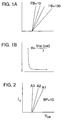
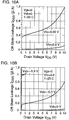
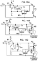
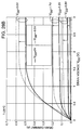
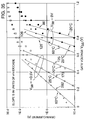
- Second, and more important, the output characteristics of a saturated BJT are equivalent to a voltage source and a resistor connected in series, both of which vary as a function of the base drive current. Deep in saturation the voltage source represents a 200 mV offset voltage, and at larger base currents the offset voltage increases. As shown in Fig. 1A, when the BJT operates as a switch, the voltage drop across the device increases as a function of both the collector current and the base current. The value FB in Fig. 1A refers to the "forced beta", or Ic/Ib. For slight increments of Vce above 0.2 V, the current increases substantially and the effective resistance (Vce/Ic) drops precipitously (see Fig. 1B). At or below 0.2 V the device exhibits an extremely high resistance (approaching that of an open circuit) despite the large base drive.
- Fig. 2 indicates that increasing the area of the BJT lowers the resistance of the device, but the offset voltage remains fixed at about 0.2 V. It is apparent, then, that switch-mode operation at a supply voltage of less than 200 mV is not possible with a BJT.
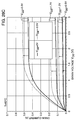
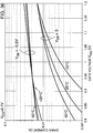
- Figs. 3A and 3B show that MOSFETs do not suffer from the series voltage problem, since all of the Id/Vds curves originate at the origin. The vertical axis in Fig. 3A represents Id and the vertical axis in Fig. 3B represents log Id. Both sets of curves show that Id increases in proportion to Vds until the device saturates (hence the name "linear" region). The reciprocal of the slope of the Id/Vds curves in the linear region is the on-resistance Rds(on), which is constant and essentially independent of Id for a given gate drive. This contrasts with the

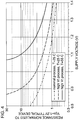
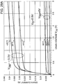
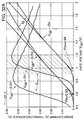
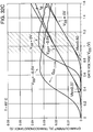
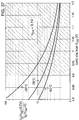
- The main problem with a MOSFET is that the gate voltage required to turn it on, referred to as the threshold voltage Vt, is more difficult to control in manufacturing than the turn-on voltage of a BJT. Vt variations of ±150 mV around a nominal value are common. The result is that the value of Rds(on) is extremely difficult to predict. This is shown in Fig. 4, which shows a plot of on-resistance (normalized to the on-resistance of a typical MOSFET having a Vt of 0.8 V with its gate biased at a Vgs of 1.2 V) as a function of the gate drive Vgs. Curve P1 represents a nominal device operating at a temperature of 25 °C. As indicated, the resistance at a Vgs of 0.9 V is about 2.5 times the resistance at a Vgs of 1.2 V. Curve P2 represents a device (again operating at 25 °C) which, owing to manufacturing variations, has a Vt which is 150 mV higher. The normalized resistance of this device is 1.5 at a Vgs of 1.2 V and 10 at a Vgs of 0.9 V. Finally, curve P3 represents the second device operating at -55 °C. With this high Vt process Vt shifts at a rate of 3 mV/°C. As shown, the resistance at a Vgs of 1.2 V is 3.4, and at a Vgs of 0.9 V is off the graph.
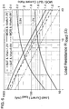
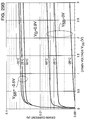
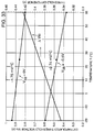
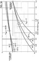
- Figs. 5A, 5B and 6 illustrate further the comparative performance of BJTs and MOSFETs. Figs. 5A and 5B illustrate circuit diagrams showing power semiconductor switches in a bridge configuration, where a push-pull output stage is used to connect each terminal of a load such as a motor. In Fig. 5A the switches are BJTs; in Fig. 5B the switches are MOSFETs. To energize the load two diagonal switches are driven simultaneously on to conduct current in a given direction. The current flow can be reversed by turning those switches off and turning the other diagonal pair of switches on. The voltage applied to the load can be considered AC with its peak-to-peak swing being twice the supply voltage (ignoring the voltage drops across the switches).
- Unfortunately, as shown in Fig. 6, the voltage drops across the switches cannot be ignored. Fig. 6 shows a comparative graph of load current as a function of load resistance for circuits shown in Figs. 5A and 5B. In the circuit of Fig. 5A, the BJTs are assumed to have a 0.25 V drop with no incremental resistance; in the circuit of Fig. 5B, the MOSFETs are assumed to have a resistance of 300 mΩ. The current for the BJTs at supply voltages of 0.9 V and 1.2 V is represented by curves P1 and P2, respectively; the current for the MOSFETs at the same supply voltages is represented by curves P3 and P4, respectively.
- At very low load resistances, most of the supply voltage falls across the switches so that the influence of the Vce(sat) voltages of the BJTs is small. At a supply voltage of 0.9 V and a load resistance of 1 Ω, the Vce(sat) drop of 0.5 V (2 x 0.25 V) in the BJTs leaves a drop of 0.4 V across the load, resulting in a current of 400 mA. In the case of the MOSFET switches, the full 0.9 V is applied to the load, resulting in a current of 570 mA, or an increase of 50% as compared with the current through the BJTs. For a 40 Ω load, the resistance of the switches is virtually negligible. While the MOSFET circuit (Fig. 5B) conducts 22 mA (0.9 V/40 Ω), the BJTs (Fig. 5A) can deliver only 10 mA ((0.9 V - 0.5 V)/40 Ω), or less than half that of the MOSFET bridge. Note, moreover, that this comparison is unfairly weighted toward the BJT version since it would take an unreasonably large BJT to eliminate its incremental resistance.
- Fig. 6 makes it clear that in low voltage situations the performance of MOSFET switches is far superior to the performance of BJT switches. In the past, the on-resistance of power MOSFETs has been reduced by shortening the channel length, optimizing the drain doping concentration, packing more cells or gate perimeter into a given area, and lowering the threshold voltage. Once all of these techniques have been employed to achieve a minimal on-resistance for a given breakdown resistance and gate oxide thickness, practically the only technique that remains available to improve the on-resistance at low levels of Vgs is to further reduce the threshold voltage. However, as described above, process variability makes the fabrication of reproducible, extremely low Vt devices difficult. Also, MOSFET devices with extremely low threshold voltages are subject to increased channel leakage at process and temperature extremes. Thus, what is needed is a power MOSFET switch with a low on-resistance and a low threshold voltage with minimal sensitivity to process and temperature variations.
- The power MOSFET switch of this invention has a low on-resistance under "starved" gate drive conditions (e.g., a supply voltage in the range of 0.8 V - 3.0 V) and has minimal sensitivity to process variations. The MOSFET is a four-terminal MOSFET, with the source, drain, body and gate having separate terminals. The body and gate terminals are driven synchronously such that the body is partially forward-biased with respect to the electrical source when the gate is driven so as to turn the MOSFET on, i.e., the forward-bias is at a level (e.g., 0.5 V) that is not sufficient to cause a significant forward current to flow through the PN junction between the body and electrical source. When the power MOSFET is turned off, the body is preferably shorted to the electrical source so as to minimize the leakage current in the off state. (In an N-channel device the "electrical source" is the more negative of the source/drain terminals; in a P-channel device the "electrical source" is the more positive of the source/drain terminals).
- As a result of the so-called "body effect", forward-biasing the source-body junction of the device lowers its threshold voltage in absolute terms (i.e., in an N-channel device the threshold voltage becomes less positive; in a P-channel device the threshold voltage becomes less negative). The source-body junction can be forward-biased by using an clamped or unclamped body bias voltage supplied by the gate, through a resistor or current source. Alternatively, the body bias can be generated by a separate body bias buffer with or without a means of limiting the maximum body bias when the MOSFET is turned on.
- The body effect in the MOSFET is enhanced by overdoping the body (which may be in an epitaxial layer or a well) and by introducing a shallow threshold adjust implant in the channel or the gate oxide layer to reduce the threshold voltage (absolute value) of the MOSFET.
- The MOSFET of this invention may be lateral or double-diffused (lateral, quasi-lateral or vertical), and it may be planar or trench-gated.
- Fig. 1A illustrates a graph showing the output characteristic of a saturated bipolar transistor for various values of Ic/Ib.
- Fig. 1B illustrates a graph showing the collector-emitter resistance of a saturated bipolar transistor as a function of Vce.
- Fig. 2 illustrates a graph showing the effect of area scaling on the resistance Rce of a bipolar transistor.
- Figs. 3A and 3B illustrate graphs showing the I-V characteristics of a MOSFET.
- Fig. 4 illustrates a graph showing the normalized on-resistance of a MOSFET as a function of supply voltage at three different temperatures.
- Figs. 5A and 5B illustrate circuit diagrams of an H-bridge circuit containing bipolar transistors and MOSFETs, respectively.
- Fig. 6 illustrates a graph showing the load current and ratio of load currents for the circuits shown in Figs. 5A and 5B.
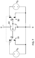
- Fig. 7 illustrates a basis circuit diagram of a MOSFET constructed in accordance with this invention.
- Fig. 8 illustrates a graph showing the threshold voltage of a MOSFET as a function of the source-body bias at different level of body dopant concentration.
- Fig. 9 illustrates a graph similar to the graph of Fig. 8 after a threshold adjust implant has been performed to reduce the threshold voltage of the MOSFET.
- Fig. 10A illustrates a graph showing the leakage current in the off-state of a MOSFET as a function of the voltage across the device at two levels of threshold voltage.
- Fig. 10B illustrates a graph showing the leakage current in the off-state of a MOSFET as a function of the voltage across the device at three levels of body bias.
- Figs 11A-11C illustrate timing diagrams showing, in particular, the behavior of the body voltage and the threshold voltage as a MOSFET in accordance with this invention is switched from off to on.
- Fig. 11D illustrates a circuit diagram of a MOSFET in accordance with this invention.
- Fig. 12A illustrates a circuit diagram of a MOSFET in which the body bias is derived form the gate bias using a current-limiting resistor.
- Fig. 12B illustrates a circuit diagram of a MOSFET in which the body bias is derived form the gate bias using a current-limiting resistor and a Schottky diode clamp.
- Fig. 12C illustrates a circuit diagram of a MOSFET in which the body bias is derived form the gate bias using a current-limiting resistor and a pseudo-Schottky diode clamp.
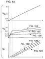
- Fig. 13 illustrates a graph showing the behavior of the body voltage and body current in the MOSFETs of Figs. 12A-12C as the gate voltage is increased over time.
- Fig. 14A illustrates a circuit diagram of a MOSFET in which the body bias is derived from the gate bias using a current-limiting depletion mode MOSFET.
- Fig. 14B illustrates a circuit diagram of a MOSFET in which the body bias is derived from the gate bias using a current-limiting depletion mode MOSFET and a Schottky diode clamp.
- Fig. 14C illustrates a circuit diagram of a MOSFET in which the body bias is derived from the gate bias using a current-limiting depletion mode MOSFET and a pseudo-Schottky diode clamp.
- Fig. 15 illustrates a graph showing a comparison between the base current in the embodiments shown in Figs. 12A-12C and the embodiments shown in Figs. 14A-14C as a function of the gate drive voltage.
- Fig. 16A illustrates a circuit diagram of a MOSFET in which a depletion mode MOSFET is used to short the body to the source when the device is turned off.
- Fig. 16B illustrates a circuit diagram similar to Fig. 16A further including a second depletion mode MOSFET for limiting the body current.
- Fig. 16C illustrates a circuit diagram similar to Fig. 16B further including a pseudo-Schottky diode as a clamp between the body and source of the main power MOSFET.
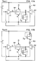
- Fig. 17A illustrates a circuit diagram of a MOSFET in which both the gate drive and body bias are derived from a separate voltage supply line using a pair of inverters and a resistor.
- Fig. 17B illustrates a circuit diagram of a MOSFET in which both the gate drive and body bias are derived from a separate voltage supply line using a pair of inverters and a pseudo-Schottky diode.
- Fig. 18 illustrates a circuit diagram of a MOSFET in which both the gate drive and body bias are derived from a separate voltage supply line using a pair of inverters and a pair of series-connected N-channel MOSFETs.
- Fig. 19 illustrates a circuit diagram of a MOSFET in which both the gate drive and body bias are derived from a separate voltage supply line using a pair of inverters and voltage divider including a pair of pseudo-Schottky diodes.
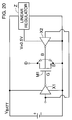
- Fig. 20 illustrates a circuit diagram of a MOSFET in which both the gate drive and body bias are derived from a separate voltage supply line using a pair of inverters and a linear regulator.
- Fig. 21 illustrates a cross-sectional view of a lateral MOSFET in accordance with this invention.
- Fig. 22 illustrates a cross-sectional view of a lateral MOSFET in accordance with this invention including a drifted drain for tolerating higher drain voltages.
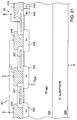
- Fig. 23A illustrates a cross-sectional view of a vertical double-diffused MOSFET in accordance with this invention.
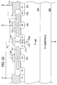
- Fig. 23B illustrates a three-dimensional cross-sectional view of a modified version of the MOSFET of Fig. 23A.
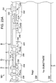
- Fig. 24 illustrates a cross-sectional view of a vertical trench-gated MOSFET in accordance with this invention.
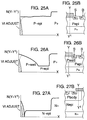
- Fig. 25A illustrates a graph showing a profile of the dopant concentration along the axis Y-Y' of the lateral MOSFET of Fig. 25B formed in an epitaxial layer.
- Fig. 26A illustrates a graph showing a profile of the dopant concentration along the axis Y-Y' of the lateral MOSFET of Fig. 26B formed in a well.
- Fig. 27A illustrates a graph showing a profile of the dopant concentration along the axis Y-Y' of the double-diffused MOSFET of Fig. 27B.
- Figs. 28A-28C illustrate graphs showing drain current as a function of gate voltage in conventional and body-biased MOSFETs at temperatures of -20° C, 25° C and 60° C, respectively.
- Figs. 28D and 28E are detailed views showing portions of the graphs illustrated in Figs. 28A and 28B.
- Figs. 29A and 29B illustrate graphs showing drain current as a function of drain voltage in conventional and body-biased MOSFETs at temperatures of -20° C, 25° C and 60° C, respectively, and at a gate voltage of 0.9 V.
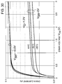
- Fig. 30 illustrates a graph showing drain current as a function of drain voltage in conventional and body-biased MOSFETs at temperatures of -20° C, 25° C and 60° C, respectively, and at a gate voltage of 1.2 V.
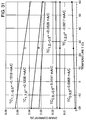
- Fig. 31 illustrates a graph showing drain current as a function of temperature at various levels of gate drive and body bias.
- Figs. 32A-32C illustrate graphs showing drain current and transconductance as a function of gate voltage for conventional and body-biased MOSFETs at temperatures of -20° C, 25° C and 60° C, respectively.
- Fig. 33 illustrates a graph showing the extrapolated threshold voltage as a function of temperature for conventional and body-biased MOSFETs as well as the difference between the extrapolated threshold voltages for the two types of devices.
- Fig. 34 illustrates a graph showing the subthreshold drain current as a function of gate voltage for conventional and body-biased MOSFETs at temperatures of -20° C, 25° C and 60° C, respectively, at a drain voltage of 0.1 V.
- Fig. 35 illustrates a graph showing the slope of the curves shown in Fig. 34.
- Fig. 36 illustrates a detailed graph similar to the graph of Fig. 34 for a range of gate voltages from 0.8 V to 1.2 V.
- Fig. 37 illustrates a graph showing the ratio of drain currents in conventional and body-biased MOSFETs at temperatures of -20° C, 25° C and 60° C, respectively, at a drain voltage of 0.1 V.
- Fig. 38 illustrates a graph similar to the graph of Fig. 36 normalized for the drain current for the conventional MOSFET at a gate voltage of 1.2 V.
- Fig. 39A illustrates a graph showing the resistivity of conventional and body-biased MOSFETs as a function of gate voltage at temperatures of -20° C, 25° C and 60° C.
- Fig. 39B illustrates a detailed view of a portion of the graph of Fig. 39A.
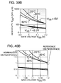
- Figs. 40A and 40B illustrate graphs showing the on-resistance of conventional and body-biased MOSFETs as a function of gate voltage at temperatures of -20° C, 25° C and 60° C.
- Fig. 41 illustrates a graph showing the ratio of the on-resistance of conventional and body-biased MOSFETs as a function of gate voltage at temperatures of -20° C, 25° C and 60° C.
- This invention uses an intentionally forward-biased body-source junction to produce a power MOSFET which has a low threshold voltage (absolute value) and which therefore can be used at very low operating voltages. A primary objective of forward-biasing the source-body junction is to reduce the on-resistance of the power MOSFET when it is used as a switch element, not to alter the small signal transconductance of the device.
- The basic principle of this invention is illustrated in Fig. 7. MOSFET M1 has a drain terminal D, a source terminal S, a gate terminal G, and a body terminal B. Since MOSFET M1 is an N-channel MOSFET, the drain terminal D is biased positively with respect to the source terminal S. Single-pole, double-throw switches S1 and S2 are ganged together such that when MOSFET M1 is turned on by biasing the gate terminal G to a positive voltage VG, the body terminal B is biased positively by a voltage VB with respect to the source terminal S. Since MOSFET M1 is an N-channel MOSFET, its body includes P-type material while its source includes N-type material. Therefore biasing the body terminal B positively with respect to the source terminal S forward-biases the junction between the body and source of MOSFET M1. The magnitude of the body bias voltage VB can vary, but ideally VB should result in minimal minority carrier injection. In practice, at room temperature this limits VB to voltages under 0.7V. Forward-biasing the source-body junction of MOSFET M1 in this way lowers the threshold voltage Vt of MOSFET M1.
- Thus the act of turning on MOSFET M1 automatically reduces the threshold voltage of MOSFET M1, which by definition is the minimum voltage at which the MOSFET can be turned on. In this way, VG can be reduced to a level below that which would be required if the source body junction of MOSFET M1 were not forward-biased. Assuming that VG is the supply voltage that is available in the circuity in which MOSFET M1 is connected, this in effect means that MOSFET M1 can be used with lower supply voltages. Moreover, the on-resistance of MOSFET M1 will be lower at a given level of VG. The body bias supply VB will typically be less than VG since VB should be limited to 0.7 V and VG is always set at the maximum available gate drive. In principle, then, VB can be derived from the same source as VG, but it may also be derived from an independent source.
- To turn MOSFET M1 off, switches S1 and S2 are thrown so as to connect the gate terminal G and the body terminal B to the source terminal. This removes the gate drive voltage VG and simultaneously increases the threshold voltage of MOSFET M1 by removing the body bias voltage VB. Alternatively, MOSFET M1 can be turned off by reversing the polarity of the gate voltage, but normally it is more convenient to reduce the gate-to-source voltage VGS to zero.
- The following equation expresses the threshold voltage Vt of MOSFET M1 as a function of the source-to-body voltage VSB:


- According to Tsividis, The MOS Transistor, McGraw-Hill, New York (1987), the bulk voltage ΨB in turn is defined by the following relationship:


- Fig. 8 illustrates a graph showing the variation of the threshold voltage as a function of the voltage VSB across the source-body junction. Positive values of VSB indicate a reverse bias and negative values of VSB indicate a forward bias. The thickness of the gate oxide of the MOSFET was 400 Å. The curve designated NB1 represents the threshold voltage with the body doped to a concentration of 1 X 1016 cm-3 with a threshold adjust implant of 2.8 X 1011 cm-2, which yields a threshold voltage Vto of 0.7 V when VSB is equal to zero. The curves designated NB2 and NB3 represent the threshold voltage when the body concentration is increased to 5 X 1016 cm-3 and 1 X 1017 cm-3, respectively, with the other factors held constant. As indicated, the threshold voltage increases with increasing values of VSB. Fig. 8 indicates that the threshold voltage varies only slightly with a body doping concentration of 1 X 1016 cm-3 while the variation increases with increasing body doping concentration. However, when the body doping concentration is increased, the value of the threshold voltage increases significantly.
- The data shown in Fig. 8 can be derived mathematically by differentiating equation (1) as follows:

- Equations (6) and (7) indicate that increasing the body doping level NB increases the derivative dVt/dVSB, thereby increasing the benefits of partially forward-biasing the source-body junction.
- The natural threshold voltage Vto is given by:


- This indicates that the natural threshold Vto is also a function of the body doping concentration NB. Thus equations (6) and (9) confirm the data shown in Fig. 8, namely, that the benefits of a higher body effect and greater threshold voltage shift (dVt/dVsb) are offset by a higher threshold voltage Vt.
- To limit the increase in the threshold voltage which results from a high body doping concentration, a thick oxide layer or a large value of γ, the channel must be counter-doped with a shallow threshold adjust implant. The magnitude of the threshold adjust implant is given by:

- As noted above, the curves in Fig. 8 were shifted downward by a threshold voltage adjust implant (e.g., phosphorus or arsenic at a dosage of 2.8 X 1011 cm-2).
- Rearranging equation (11) yields:

- Accordingly, the device represented by curve NB1 had a threshold of 0.7 V + 0.519 V = 1.219 V prior to the threshold adjust implant. While the device is represented by curves NB2 and NB3 were also shifted downward by 0.519V as a result of the threshold adjust implant, the threshold voltages of these devices are still too high to be useful.
- To compensate for the increased threshold voltage which accompanies a higher dVt/dVSB, the dosage of the threshold adjust implant must be increased. Fig. 9 illustrates how raising the threshold adjust implant can be used to increase dVt/dVSB without increasing the threshold voltage itself. The devices represented by curves NB1, NB2 and NB3 in Fig. 9 have the same body dopant concentrations and gate oxide layer thicknesses (400 Å) as the devices represented by the corresponding curves in Fig. 8. It is noteworthy that the threshold voltage for the device represented by curve NB3 approaches zero at


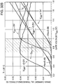
- While Fig. 9 illustrates how a low threshold voltage can he induced electrically, the resulting devices are not equivalent to a device fabricated with an extremely low natural threshold voltage. The cost of inducing a low threshold voltage is increased leakage when the device is in its off condition. Fig. 10A illustrates a graph showing the leakage current in the off state (IDSS) as a function of the voltage across the device (VDS) at two levels of Vto (0.65 V and 0.8 V) when T = 60° C and


- Fig. 10B illustrates a graph showing IDSS as a function of VDS at three levels of body bias VSB when T = 25° C,


- Figs. 10A and 10B clearly indicate that to insure low off-state current leakage a device must have a Vto greater than 0.65 V (ideally between 0.7 and 0.8 V) at room temperature and must have a

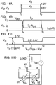
- The solution to this problem is to switch the body synchronously with the gate, so that a forward-bias is applied to the source-body junction when the device is turned on, while the body is shorted to the source when the device is turned off. The switching process is illustrated in Figs. 11A-11D. Fig. 11D is similar to Fig. 7 and shows MOSFET M1 connected to control the power to a load. The circuit is supplied by a voltage source VDD. The gate of MOSFET M1 is controlled by switch S1, and the body of MOSFET M1 is controlled by switch S2.
- Figs. 11A-11D show the results of turning MOSFET M1 on at a time t1 and turning it off at a time t2. As shown in Fig. 11A, the gate voltage VG is increased to 1.2V and the body voltage VB is increased to 0.5V at the time that MOSFET M1 is turned on. As shown in Fig. 11B, the drain current ID increases when MOSFET M1 is turned on, and the voltage across MOSFET M1 falls from the supply voltage VDD to a voltage which is determined by the on-resistance RDS of MOSFET M1. The small leakage current that flows when MOSFET M1 is turned off is not shown in Fig. 11B. Fig. 11C shows that the threshold voltage falls from 0.7 V when MOSFET M1 is turned off to a threshold voltage in the range of 0.01-0.4 V when MOSFET M1 is turned on. This results from using switch S2 to apply a forward-bias to the source-body junction of MOSFET M1 when it is turned on. As indicated in Fig. 11B, switches S1 and S2 are ganged together so that the source-body bias is applied synchronously with the gate drive which turns MOSFET M1 on.
- There are numerous circuits that can be used to obtain a forward-biased source-body junction in the MOSFET. For example, in a discrete device typically only three voltage levels are available--gate, source and drain voltages--and the body potential must be derived from one of these voltages.
- A solution to the problem is shown in Fig. 12A, where a resistor R1 is connected between the gate and body terminals of the MOSFET M1. Increasing the gate voltage VG also raises the body potential VB, thereby lowering the threshold voltage of MOSFET M1. Resistor R1 acts as a current-limiting resistor which prevents the body current from reaching excessive levels. Values for R1 in the range 10kΩ to 10MΩ are possible, but values in the range of 100KΩ to a few MΩ offer a reasonable balance between the on-state body current (which ideally should be zero) and lowering the threshold voltage of the device.
- The body voltage VB of the arrangement shown in Fig. 12A is determined by a voltage divider consisting of resistor R1 and the source-body junction of MOSFET M1. Since the source-body junction acts as a PN diode, the body current IB can be expressed in terms of the voltage across the diode Vj using the well-known diode equation described in S. M. Sze, Physics of Semiconductor Devices, John Wiley & Sons (1981), pages 87-89. This results in the following equation for the body current:


- Equation (16) is an approximation which can be used for large values of RB. For a 2.3 MΩ resistor R1, for example, a 3 V gate drive would result in 1 µA of body current.
- A possible shortcoming of the circuit shown in Fig. 12A is that the resistor R1 determines the magnitude of the body current, but the maximum body voltage VB is determined by the current-voltage characteristics of the PN junction between the source and body of MOSFET M1. The voltage drop across the source-body junction maybe higher than is desirable, and in addition the forward current across the source-body junction may lead to charge storage which can increase the time it takes to turn the MOSFET off. Moreover, the body current and stored minority carrier charge may vary significantly with the gate voltage. For example, a resistor R1 chosen for a gate bias of 3 V may allow excessive currents at a gate bias of 10 V. Also, high levels of stored charge can lead to non-uniform current conduction during turn-off of the MOSFET. Finally, using a large resistor R1 to minimize the body current IB when MOSFET M1 is turned on results in a nearly floating base when MOSFET M1 is turned off, and when higher drain voltages may be present. The floating base results in a BVceo-type breakdown which maybe a small fraction of the ideal BVdss diode breakdown.
- The maximum body voltage and current may be intentionally limited by clamping the body voltage as in the arrangements shown in Figs. 12B and 12C. In 12B, a Schottky diode D1 is connected in parallel with the source-body junction. Depending on the value of resistor R1, Schottky diode D1 could limit the body voltage to a voltage in the vicinity of 0.2 V. In the arrangement shown in Fig. 12C, a pseudo-Schottky diode D2 has been used to clamp the body of MOSFET M1. Pseudo-Schottky diode D2 is a MOSFET whose source, body and gate terminals are connected together, in accordance with the teachings of the above-referenced Application Serial No. 08/648,334. An advantage of this embodiment is that the pseudo-Schottky diode can be integrated with MOSFET M1. In the arrangements shown in Fig. 12B and 12C, the clamping device must have a lower voltage than the voltage across the source-body junction of MOSFET M1, or the source-body junction of the MOSFET itself may conduct an equal or greater current than the clamp. The forward voltage of the Schottky diode D1 and psuedo-Schottky diode D2 track that of the PN diode (source-body junction) with temperature. Increasing the temperature decreases the VBE of the PN diode but likewise decreases the voltage across the pseudo-Schottky diode D2, thereby avoiding conduction in the PN diode.
- The graphs shown in Fig. 13 illustrate what happens to the body voltage VB and body current IB as the gate voltage VG is increased linearly with time. The three curves for VB and IB represent the arrangements of Figs. 12A-12C. As indicated, the body voltage VB is clamped at about 0.2 V with a Schottky diode clamp (Fig. 12B), at about 0.4 V with a pseudo-Schottky clamp (Fig. 12C), and at about 0.6 V with no clamp (Fig. 12A). As soon as the clamping potential is reached, in each instance the body current increases almost linearly with increasing VG. Because the clamp limits the maximum body voltage, however, the current and stored charge in the source-body diode of MOSFET M1 is reduced.
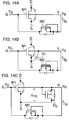
- The body current at relatively high gate voltages can be lowered by using a depletion mode MOSFET as a current limiter. Figs. 14A-14C illustrate arrangements that are identical to those shown in Figs. 12A-12C except that in each case the current limiting resistor R1 has been replaced by an N-channel depletion mode MOSFET M2. The gate and source terminals of depletion mode MOSFET M2 are tied together. For small values of VG, depletion mode MOSFET M2 acts as a resistor having a resistance of


- Fig. 15 illustrates the body current as a function of the gate voltage for the clamped circuits shown in Figs. 12A-12C and the clamped and current-limited circuits shown in Figs. 14A-14C. It is immediately apparent that the current-limiting depletion mode MOSFET M2 reduces the body current at a high gate bias to a small fraction of what it would be with a current-limiting resistor. The extent of this reduction can be estimated by assuming a depletion mode MOSFET with a linear resistance RDs(on) equal to the resistance RB of the resistor R1:

- This results in a body current IB of:

- A depletion mode MOSFET of this size, when saturated, conducts a current of:

- Taking the ratio of equation (18) to equation (19) yields the ratio of the body currents in the embodiments shown in Figs. 12A-12C and 14A-14C, respectively:

- For example, comparing the embodiments shown in Figs. 12C and 14C and assuming a 0.5 V pinchoff voltage for depletion mode MOSFET M2 and a 0.4 V clamping voltage for pseudo-Schottky diode D2, the current at a gate voltage VG of 10.4V is 10 times larger in the embodiment of Fig. 12C. This assumes that resistor R1 has a resistance value comparable to that of depletion mode MOSFET M2.
- As indicated above, the body and source of MOSFET M1 should be shorted together when the device is turned off in order to minimize leakage currents. Figs. 16A-16C illustrate several circuits for accomplishing this. The circuit shown in Fig. 16A is similar to the circuits of Figs. 12B and 12C, with the addition of a P-channel depletion mode MOSFET M3 connected between the source and body terminals of MOSFET M1. When VG is pulled high to turn MOSFET M1 on the gate voltage of PMOSFET M3 rises to a level above the source voltage of PMOSFET M3. Thus PMOSFET M3 turns off, allowing the source-body junction of MOSFET M1 to become forward-biased. The body voltage VB is limited by a clamping device CL which could be the Schottky diode D1 or the pseudo-Schottky diode D2 shown in Figs. 12B and 12C. When VG is reduced to turn off MOSFET M1, PMOSFET M3 turns on, thereby shorting the source and body of MOSFET M1 together.
- Fig. 16B shows an alternative version which includes the current limiting depletion mode NMOSFET M2 of Figs. 14A-14C, which as described above limits the body current after the clamping device CL becomes operative. Fig. 16C shows a similar circuit with the pseudo-Schottky diode D2 used as the clamping device.
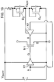
- In the embodiments shown in Figs. 12A-12C, 14A-14C and 16A-16C, the body bias VB is derived from the gate terminal of the power MOSFET. These embodiments are particularly appropriate for the manufacture of a discrete device, in which only the source, drain and gate voltages are available. If a separate supply line, typically referred to as Vbatt or Vcc is available, the body bias may be derived from the supply line rather than from the gate terminal of the MOSFET. As a result, the gate terminal draws no current. Figs. 17A, 17B and 18-20 illustrate several embodiments which use a separate supply line to produce the body bias.
- In the embodiment of Fig. 17A, the gate and body of MOSFET M1 are connected to the outputs of inverters X1 and X2, respectively. A battery provides a supply voltage Vbatt. Vbatt is connected directly to the high-side power input to inverter X1 and through a current-limiting resistor R2 to the high-side power input to inverter X2. MOSFET M1 is turned on by pulling the input to inverter X1 low which essentially connects Vbatt to the gate of MOSFET M1. The output of inverter X2 is Vbatt less the voltage drop across resistor R2, which is delivered at the output of inverter X2. As in several of the embodiments previously described, pseudo-Schottky diode D2 clamps the body voltage of MOSFET M1, producing the desired voltage drop across the source-body junction of MOSFET M1. MOSFET M1 is turned off by pulling the inputs to inverters X1 and X2 high, which shorts the source, body and gate terminals of MOSFET M1 together. The embodiment shown in Fig. 17B is similar, except that a second pseudo-Schottky diode D3 is substituted for the current-limiting resistor R2. Optionally, a small resistor R3 may be connected in series with pseudo-Schottky diode D3, to limit the current in the pseudo-Schottky diode. Since a pseudo-Schottky diode typically turns on at about 0.4V the output of inverter X2 is at a voltage approximately equal to Vbatt less 0.4V.
- The inverters X1 and X2 in Figs. 17A and 17B are typically CMOS inverters which include a series-connected PMOSFET and NMOSFET. In Fig. 18, the CMOS pair of inverter X2 is replaced by a pair of NMOSFETS M4 and M5, with the high side NMOSFET M5 acting as a source follower. A second inverter X3 is connected between the output of inverter X1 and the gate of MOSFET M1. MOSFET M1 is turned on by pulling the input to inverter X1 high, which raises the gate voltage of MOSFET M1 to Vbatt. Since the input to inverter X1 is connected to the gate of NMOSFET M5, NMOSFET M5 is turned on; conversely, the output of inverter X1 is connected to the gate of NMOSFET M4, and this turns NMOSFET M4 off. Thus, the body of MOSFET M1 sees a voltage which is limited to a threshold drop below the gate drive of MOSFET M1. MOSFET M1 is turned off by pulling the input to inverter X1 low, which turns NMOSFET M4 on and shorts the source and body terminals of MOSFET M1 together.
- In the embodiment of Fig. 19, a pair of pseudo-Schottky didoes D3 and D4 form a voltage divider which supplies a voltage Vaux to the high-side power input of inverter X2. Thus, when MOSFET M1 is turned on by lowering the inputs to inverters X1 and X2, inverter X2 delivers a body bias which is approximately equal to Vbatt less the voltage drop across pseudo-Schottky diode D3, or about 0.4V. The embodiment of Fig. 20 is similar, except that a linear regulator Z has been substituted for the voltage divider consisting of pseudo-Schottky diodes D3 and D4. In this embodiment, linear regulator Z supplies an output equal to 0.5 V, which is delivered to the body of MOSFET M1 when it is turned on. To operate at low input voltages (e.g., down to 0.8 V), linear regulator Z must be of the low-dropout type.
- While the influence of the body terminal in lowering the threshold voltage has been mentioned in the semiconductor literature (e.g., S.M. Sze, Physics of Semiconductor Devices, 2nd ed., John Wiley & Sons (1981), p. 462), and while body biasing has been used in some very low voltage circuits such as watch circuits, the use of this technique in high-power switches to reduce on-resistance under "starved gate" drive conditions is new and raises issues and concerns not previously encountered. In particular, the construction of a power MOSFET for "starved gate" drive operation requires the combination of several features to offer acceptable performance at extremely low input voltages. These features include: maximizing the gate perimeter per unit area of the device, and providing a short channel length and a low series drain resistance. Beyond this, generating a high body effect and low threshold voltage requires the same design considerations that are described in connection with the pseudo-Schottky diode in the above referenced Application Serial No. 08/648,334.
- In fabricating a four-terminal MOSFET in accordance with this invention, the body is formed with a high dopant concentration and is then counter-doped using some threshold adjust technique. The higher the body dopant concentration NB, the higher the dosage of the threshold adjust implant must be. However, a high body dopant concentration and threshold adjust implant yield a device which provides superior performance at low operating voltages.
- Figs. 21, 22, 23A, 23B, and 24 illustrate cross sectional views of various embodiments of a four-terminal MOSFET M1 in accordance with this invention. Fig. 21 shows MOSFET M1 in a lateral version. An
N+ source region 200 and anN+ drain region 202 are formed in a P-epitaxial layer 204. P-epitaxial layer 204 overlies aP+ substrate 206. The current flow betweensource region 200 and drainregion 202 is controlled by agate 207.Source region 200 and drainregion 202 are contacted by metal contact layers 209 and 211, respectively. - Pseudo-Schottky diode D2 used as a body clamp includes an
N+ source region 208 which is shorted to a P+body contact region 210 by ametal contact layer 212. As shown, source region and body contact region are shorted to thegate 214 of pseudo-Schottky diode D2 as described in the above referenced Application Serial No. 08/648,334, the channel of pseudo-Schottky diode D2 conducts when the voltage at source region 208 (anode) exceeds the voltage at the drain (cathode) of the pseudo-Schottky diode (which is also the source of MOSFET M1) by a voltage in the range 0.3-0.5 V. Pseudo-Schottky diode D2 accordingly insures that the body voltage of MOSFET M1 does not exceed the source voltage of MOSFET M1 by more than 0.3-0.5 V. - Fig. 22 shows a similar embodiment with the difference that the N+ drain region of MOSFET M1 is provided with an N- "drift"
region 216.Drift region 216 allows the device to tolerate higher drain voltages (e.g. 12-100 V) than the undrifted version shown in Fig. 21. - Fig. 23A shows a cross sectional view of a four-terminal vertical planar DMOSFET according to this invention. In this embodiment, MOSFET M1 is formed in an N-
epitaxial layer 230 which overlies anN+ substrate 232.N+ substrate 232 serves as the drain of MOSFET M1. MOSFET M1 also includes aP body region 234 andN+ source region 236 and a P+body contact region 238. A channel region is formed inP body 234 under agate 240. Pseudo-Schottky diode D2 includes aP body 242, andN+ source region 244, a P+body contact region 246, and anN+ drain region 248, which is connected to theN+ source region 236 of MOSFET M1. As shown, thebody region 242 andsource region 244 of pseudo-Schottky diode D2 are tied through a metal layer to agate 250. - Fig. 23B illustrates a three-dimensional view of a modified version of the embodiment of Fig. 23A. DMOSFET M1 includes a P-
body region 234A, anN+ source region 236A and agate 240A. Contact with P-body region 234A is made in the third dimension by means of aP+ contact region 238A. Pseudo-Schottky diode D2 includes anN+ source region 244A and a P+body contact region 246A, which provides contact with a P-body region 242A. P+body contact regions gate 250A of pseudo-Schottky diode D2. Pseudo-Schottky diode D2 also includes anN+ drain region 248A, which is tied toN+ source region 236A. An arm ofgate 250A controls the current flow inchannel regions 252, which actually form a part of MOSFET M1. Sincegate 250A would not be driven as high asgate 240A, the current throughchannel regions 252 would not be as large as the current in the channel regions lying undergate 240A. This modest penalty is more than compensated for, however, by the efficient use of the surface area of the chip. The current in pseudo-Schottky diode D2 flows laterally betweenN+ source region 244A andN+ drain region 248A. - Fig. 24 illustrates a cross sectional view of a trench-gated version of MOSFET M1. The MOSFET is formed in an N-
epitaxial layer 260 overlying anN+ substrate 262, which serves as the drain of the device. Thegate 266 is formed in a series of trenches at the top surface of N-epitaxial layer 260. MOSFET M1 also includes a P-body region 262 and anN+ source region 264. Pseudo-Schottky diode D2 includes aP body region 263, a P+body contact region 264, anN+ source region 266 and anN+ drain region 268, the latter being connected to theN+ source region 264 of MOSFET M1. P+body contact region 264 andN+ source region 266 are connected through a metal layer to adrain 270 of pseudo-Schottky diode D2. As shown, in the third dimension the source-body-gate (anode) terminal of pseudo-Schottky diode D2 is connected via a wire or other conductive path to a P+body contact region 272 at the top surface of the device, which adjoinsP body region 262. In this way, the anode of pseudo-Schottky diode D2 is connected to the body of MOSFET M1. Also, as shown, theN+ drain region 268 of pseudo-Schottky diode D2 is tied to theN+ source region 264 of MOSFET M1. - Fig. 25A shows a dopant profile of the lateral MOSFET shown in cross-section in Fig. 25B (which is similar to the lateral MOSFET of Fig. 21), taken along the Y-Y' axis. The vertical axis of Fig. 25A corresponds to the surface of the MOSFET and the horizontal axis represents the distance below the surface. As shown, the P-epitaxial layer is doped quite heavily (e.g., to a resistivity of from 40 to 3 mΩ-cm) and a shallow threshold adjust implant is introduced at the surface to lower the threshold voltage of the MOSFET.
- Figs. 26A and 27A are similar dopant profiles of the dopant concentrations of the MOSFETs shown in Figs. 26B and 27B along the Y-Y' axes. The MOSFET of Fig. 26B is a lateral MOSFET formed in a P-well. As shown in Fig. 26A, the P-well is heavily doped in comparison to the P-epitaxial layer, and again this heavy dopant concentration is countered by a shallow threshold adjust implant at the surface of the MOSFET. The MOSFET of Fig. 27B is a DMOSFET similar to the MOSFET shown in Fig. 23A. The P body is doped heavily but is counterdoped by a threshold adjust implant. Figs. 25A-27A illustrate the general principle that the body effect is maximized by doping the body to a heavy concentration NB, and then the threshold voltage is adjusted downward by introducing a shallow threshold adjust implant at the surface of the channel region.
- Figs. 28A-28C illustrate the behavior of the drain current as a function of the drain voltage (VDS) in a MOSFET of this invention at temperatures of -20° C, 25° C and 60° C, respectively. In one set of curves (solid lines) the source and body are shorted together (


- The situation with low drain currents is more clearly shown in Figs. 28D and 28E, which show the drain currents at -20° C and 25° C, respectively, for a VGS equal to 0.9 V and 1.2 V. The arrows indicate the shift of the drain current upward from the condition where


- Figs. 29A and 29B show the drain current as a function of VDS at temperatures of -20° C, 25° C and 60° C and for source-body voltages of 0 V and -0.5 V. Fig. 29A is plotted on linear paper and Fig. 29B is plotted on semilog paper. Without body biasing, the maximum current at any temperature is less than 5 mA, and the magnitude of the current increases with increasing temperature. This occurs because the threshold voltage decreases with increasing temperature. One disadvantage of a positive temperature coefficient of current is the risk of hot spot formation in the device, as the hotest areas conduct the most current.
- In contrast, with body biasing, the peak current ranges from 27 mA to 40 mA and decreases with increasing temperature. This occurs because, in the body biased condition, the sensitivity of the current to threshold voltage is reduced, and the decrease in the carrier mobility with increasing temperature becomes the dominant mechanism. While the variation of the drain current with temperature appears greater in the body biased case, on a percentage basis it varies by only ± 15%. Viewing the same data on semilog paper in Fig. 29B, with no body bias the saturation current varies by +39% as the temperature increases from 25° C to 60° C and by -99% as the temperature falls from 25° C to -20° C. In other words, at the cold temperature the device nearly turns off when

- Fig. 30, which is similar to Fig. 29B except that

- Fig. 31 shows a graph of the drain current as a function of temperature in the linear region of the device. ( The curves are identified by the designation "TCx,y" where x is the gate voltage VGS and y is the body bias VBS.) The curves for

- To understand the variation of drain current with temperature we must consider that the equation for drain current has two terms with pronounced temperature dependence--carrier mobility µ(T) and threshold voltage Vto(T). An increase in temperature lowers the carrier mobility which tends to decrease the drain current. This decrease is partially or completely counterbalanced by an increase in the effective gate overdrive term (VGS - Vt) resulting from the reduction in the threshold voltage (Vt) which accompanies higher temperatures. Which term is dominant depends on the value of VGS which acts as a weighing factor between the two terms. Specifically, the drain current (ID) is expressed as a function of µ(T) and Vto(T,VSB) as follows:

- From equation (23) it is apparent that a negative dµ/dT decreases the drain current and a negative dVto/dT increases the drain current. When VGS is small the second term is important while when VGS is large the second term is negligible. To find the point where the opposing effects cancel each other we set:

- The zero temperature coefficient point is therefore a gate enhancement voltage above Vto. By reducing the value of Vto using body biasing, the temperature-independent operating point can be located near the point where

- Figs. 32A-32C show the gate characteristics of a MOSFET according to this invention in the linear region at temperatures of -20° C, 25° C and 60° C, respectively. The drain current and transconductance are shown as a function of VGS for the body-biased condition (


- Fig. 34 illustrates the full linear region subthreshold characteristics of a MOSFET at


- Like Fig. 34, Fig. 35 illustrates a plot on semilog paper of the subthreshold conduction curves of conventional and body-biased MOSFETs over a range of VGS from 0 to 1.2 V. The subthreshold slope S (given in units of mV/decade of current) illustrates the rate at which the MOSFET goes from its off-state to its on-state as a function of VGS, the steeper the slope (lower number) the better. While body-biasing adversely affects the slope by a factor of 1.5 to 2, Fig. 35 clearly shows that a lower VGS is required to turn the MOSFET on when it is body-biased.
- Fig. 36 shows a close-up of the curves shown if Fig. 34 in the region of particular interest (0.9 V - 1.2 V). Note that the curves for

- Fig. 37 illustrates the ratio of the drain currents at


- Fig. 39A shows the resistivity in kΩ-µm of the body biased and non-body biased devices at temperatures of -20° C, 25° C and 60° C. Since a MOSFET must be sized to meet a target on-resistance, the higher the resistivity the larger the required area. The resistance of a given MOSFET can be found be multiplying its geometric efficiency in packing gate perimeter W into the smallest possible area A. The resistance-area product is then

- To meet a given specification for RDS the die area needed is:

- For the same geometry (hence constant A/W) and the specified RDS(spec), halving RDSW leads to a halving of the die size. AT


- Fig. 39B illustrates a detailed view of the portion of the graph of Fig. 39A where VGS is between 0.9 V and 1.2 V.
- Fig. 40A shows the same data normalized such that the resistance of the non-body biased devices is equal to one at


- Fig. 41 uses the data of Fig. 40A to show the ratio of the performance of the body-biased and conventional devices (in terms of on-resistance) for each of the VGS and T conditions shown in Fig. 40A. Note that at


- The foregoing description is intended to be illustrative and not limiting. Many additional and modified embodiments of this invention will be apparent to those skilled in the art, and all such embodiments are intended to be covered by the following claims.
Claims (28)
- A method of switching a current on and off comprising the steps of:providing a MOSFET, the MOSFET comprising first and second regions of a first conductivity type formed in a semiconductor substrate and separated by a body region of a second conductivity type, and a gate separated from channel region within the body region by a dielectric layer, neither of the first and second regions being shorted to the body region;applying a voltage VDS across the first and second regions;applying a voltage VG(on) to the gate so as to cause a current to flow between the first and second regions through the channel region;applying a voltage VB to the body region so as to forward-bias a PN junction between the body region and the second region, the voltage VG being set at a level such that a resulting forward-bias across the PN junction is not sufficient to cause a substantial current to flow across the PN junction;applying a voltage VG(off) to the gate so as to terminate the flow of current between the first and second regions through the channel region; andremoving the voltage VB from the body region.
- The method of Claim 1 wherein the step of applying the voltage VG(on) to the gate and the step of applying the voltage VB to the body region are performed simultaneously.
- The method of Claim 2 wherein the step of applying the voltage VG(off) to the gate and the step of removing the voltage VB from the body region are performed simultaneously.
- The method of Claim 1 wherein the step of applying the voltage VG(off) to the gate and the step of removing the voltage VB from the body region are performed simultaneously.
- A power MOSFET switch for switching a currrent to a load, the power MOSFET switch comprising:a four-terminal MOSFET having first, second, gate and body terminals, no one of the terminals being shorted to any of the other terminals;a first switch connected between the first and gate terminals;a second switch connected between the first and body terminals;
wherein the first and second switches are ganged together, the first switch passing a voltage VG(on) to the gate terminal and the second switch passing a voltage VB to the body terminal when the first and second switches are in a first position, the first switch passing a voltage VG(off) to the gate terminal and the second switch removing the voltage VB from the body terminal when the first and second switches are in a second position. - The power MOSFET switch of Claim 5 wherein each of the first and second switches comprises a single-pole, double-throw switch, the first switch having a common terminal connected to the gate terminal, a first terminal connected to the voltage VG and a second terminal connected to the first terminal of the MOSFET, the second switch having a common terminal connected to the body terminal, a first terminal connected to the voltage VB and a second terminal connected to the first terminal of the MOSFET.
- A power MOSFET switch arrangement comprising:a four-terminal power MOSFET having source, drain, gate and body terminals, no one of the terminals being shorted to any of the other terminals; anda resistor connected between the gate and body terminals.
- The power MOSFET switch arrangement of Claim 7 further comprising a voltage clamping device connected between the body and source terminals.
- The power MOSFET switch arrangement of Claim 8 wherein the voltage clamping device comprises a diode.
- The power MOSFET switch arrangement of Claim 9 wherein the diode is a Schottky diode.
- The power MOSFET switch arrangement of Claim 8 wherein the voltage clamping device comprises a second MOSFET, the second MOSFET having source, gate and body terminals shorted to the body terminal of the power MOSFET and a drain terminal connected to the source terminal of the power MOSFET.
- A power MOSFET switch arrangement comprising:a four-terminal power MOSFET having source, drain, gate and body terminals, no one of the terminals being shorted to any of the other terminals; anda depletion-mode MOSFET connected between the gate and body terminals, the depletion-mode MOSFET having source, body and gate terminals shorted together.
- The power MOSFET switch arrangement of Claim 12 further comprising a voltage clamping device connected between the body and source terminals.
- The power MOSFET switch arrangement of Claim 13 wherein the voltage clamping device comprises a diode.
- The power MOSFET switch arrangement of Claim 14 wherein the diode is a Schottky diode.
- The power MOSFET switch arrangement of Claim 13 wherein the voltage clamping device comprises a second MOSFET, the second MOSFET having source, gate and body terminals shorted to the body terminal of the power MOSFET and a drain terminal connected to the source terminal of the power MOSFET.
- A power MOSFET switch arrangement comprising:a four-terminal power MOSFET having source, drain, gate and body terminals, no one of the terminals being shorted to any of the other terminals;a resistor connected between the gate and body terminals; anda depletion-mode MOSFET connected between the source and body of the power MOSFET, the depletion-mode MOSFET having source and body terminals shorted together and a gate terminal connected to the gate of the power MOSFET.
- The power MOSFET switch arrangement of Claim 17 further comprising a voltage clamping device connected between the body and source terminals.
- The power MOSFET switch arrangement of Claim 18 wherein the voltage clamping device comprises a second MOSFET, the second MOSFET having source, gate and body terminals shorted to the body terminal of the power MOSFET and a drain terminal connected to the source terminal of the power MOSFET.
- The power MOSFET switch arrangement of Claim 17 further comprising a second depletion-mode MOSFET connected between the gate and body terminals of the power MOSFET, the depletion-mode MOSFET having source, body and gate terminals shorted together.
- A power MOSFET switch arrangement comprising:a power MOSFET having source, drain, gate and body terminals, no one of the terminals being shorted to any of the other terminals;a voltage supply line;a first inverter having an output terminal connected to the gate terminal and a power input terminal connected to the voltage supply line; anda second inverter having an output terminal connected to the body terminal and a power input terminal connected through a resistor to the voltage supply line.
- The power MOSFET switch arrangement of Claim 21 further comprising a voltage clamping device connected between the body and source terminals.
- The power MOSFET switch arrangement of Claim 22 wherein the voltage clamping device comprises a second MOSFET, the second MOSFET having source, gate and body terminals shorted to the body terminal of the power MOSFET and a drain terminal connected to the source terminal of the power MOSFET.
- A power MOSFET switch arrangement comprising:a power MOSFET having source, drain, gate and body terminals, no one of the terminals being shorted to any of the other terminals;a voltage supply line;a first inverter having an output terminal connected to the gate terminal and a power input terminal connected to the voltage supply line;a second inverter having an output terminal connected to an input terminal of the first inverter and a power input terminal connected to the voltage supply line; andthird and fourth MOSFETs connected in series between the voltage supply line and ground, a common node between the third and fourth MOSFETs being connected to the body terminal of the power MOSFET, the output terminal of the first inverter being connected to the gate of the third MOSFET and the output terminal of the second inverter being connected to the gate of the fourth MOSFET.
- The power MOSFET switch arrangement of Claim 24 further comprising a voltage clamping device connected between the body and source terminals of the power MOSFET.
- A power MOSFET switch arrangement comprising:a power MOSFET having source, drain, gate and body terminals, no one of the terminals being shorted to any of the other terminals;a voltage supply line;a first inverter having an output terminal connected to the gate terminal and a power input terminal connected to the voltage supply line;a second inverter having an output terminal connected to the body terminal; anda voltage divider connected to the voltage supply line, a midpoint of the voltage divider being connected to a power input terminal of the second inverter.
- The power MOSFET switch arrangement of Claim 26 wherein the voltage divider comprises second and third MOSFETs, each of said second and third MOSFETs having source, body and gate terminals shorted together.
- A power MOSFET switch arrangement comprising:a power MOSFET having source, drain, gate and body terminals, no one of the terminals being shorted to any of the other terminals;a voltage supply line;a first inverter having an output terminal connected to the gate terminal and a power input terminal connected to the voltage supply line;a second inverter having an output terminal connected to the body terminal; anda linear regulator connected to the voltage supply line, an output terminal of the linear regulator being connected to a power input terminal of the second inverter.
Applications Claiming Priority (2)
| Application Number | Priority Date | Filing Date | Title |
|---|---|---|---|
| US08/649,747 US5689144A (en) | 1996-05-15 | 1996-05-15 | Four-terminal power MOSFET switch having reduced threshold voltage and on-resistance |
| US649747 | 2000-08-28 |
Publications (3)
| Publication Number | Publication Date |
|---|---|
| EP0808027A2 true EP0808027A2 (en) | 1997-11-19 |
| EP0808027A3 EP0808027A3 (en) | 1999-07-07 |
| EP0808027B1 EP0808027B1 (en) | 2004-12-08 |
Family
ID=24606060
Family Applications (1)
| Application Number | Title | Priority Date | Filing Date |
|---|---|---|---|
| EP97107834A Expired - Lifetime EP0808027B1 (en) | 1996-05-15 | 1997-05-14 | Four-terminal power MOSFET switch having reduced threshold voltage and on-resistance |
Country Status (3)
| Country | Link |
|---|---|
| US (1) | US5689144A (en) |
| EP (1) | EP0808027B1 (en) |
| DE (1) | DE69731857T2 (en) |
Cited By (3)
| Publication number | Priority date | Publication date | Assignee | Title |
|---|---|---|---|---|
| FR2842652A1 (en) * | 2002-07-19 | 2004-01-23 | Semiconductor Tech Acad Res Ct | COMPONENT WITH INTEGRATED SEMICONDUCTOR CIRCUIT WITH BODY POLARIZATION CIRCUIT FOR GENERATING A DIRECT POLARIZATION VOLTAGE OF WELLS OF A SUFFICIENT LEVEL |
| EP1526637B1 (en) * | 2003-10-23 | 2010-11-24 | Broadcom Corporation | Tuning RF circuits using switched inductors |
| EP3419169A3 (en) * | 2017-05-05 | 2019-05-15 | Elmos Semiconductor Aktiengesellschaft | Device for controlling an electric fuse for at least one electric consumer, in particular of a vehicle |
Families Citing this family (94)
| Publication number | Priority date | Publication date | Assignee | Title |
|---|---|---|---|---|
| KR100283839B1 (en) * | 1995-06-06 | 2001-04-02 | 니시무로 타이죠 | Semiconductor integrated circuit device |
| US6232827B1 (en) | 1997-06-20 | 2001-05-15 | Intel Corporation | Transistors providing desired threshold voltage and reduced short channel effects with forward body bias |
| US6300819B1 (en) | 1997-06-20 | 2001-10-09 | Intel Corporation | Circuit including forward body bias from supply voltage and ground nodes |
| US6218895B1 (en) | 1997-06-20 | 2001-04-17 | Intel Corporation | Multiple well transistor circuits having forward body bias |
| US6593799B2 (en) | 1997-06-20 | 2003-07-15 | Intel Corporation | Circuit including forward body bias from supply voltage and ground nodes |
| US6100751A (en) * | 1997-06-20 | 2000-08-08 | Intel Corporation | Forward body biased field effect transistor providing decoupling capacitance |
| US6166584A (en) * | 1997-06-20 | 2000-12-26 | Intel Corporation | Forward biased MOS circuits |
| EP1012971A4 (en) * | 1997-06-20 | 2000-09-20 | Intel Corp | Forward body bias transistor circuits |
| US6031702A (en) * | 1997-10-22 | 2000-02-29 | Siliconix Incorporated | Short circuit protected DC-DC converter using disconnect switching and method of protecting load against short circuits |
| US6538279B1 (en) * | 1999-03-10 | 2003-03-25 | Richard A. Blanchard | High-side switch with depletion-mode device |
| US6297686B1 (en) | 1999-05-28 | 2001-10-02 | Winbond Electronics Corporation | Semiconductor integrated circuit for low-voltage high-speed operation |
| US6515534B2 (en) | 1999-12-30 | 2003-02-04 | Intel Corporation | Enhanced conductivity body biased PMOS driver |
| US6225797B1 (en) | 1999-12-30 | 2001-05-01 | Lockheed Martin Corporation | Circuit for limiting inrush current through a transistor |
| DE10022268B4 (en) * | 2000-05-08 | 2005-03-31 | Infineon Technologies Ag | Semiconductor device with two semiconductor bodies in a common housing |
| US6680650B2 (en) * | 2001-01-12 | 2004-01-20 | Broadcom Corporation | MOSFET well biasing scheme that migrates body effect |
| US6930473B2 (en) | 2001-08-23 | 2005-08-16 | Fairchild Semiconductor Corporation | Method and circuit for reducing losses in DC-DC converters |
| US6859102B2 (en) * | 2001-09-27 | 2005-02-22 | Powerq Technologies, Inc. | Amplifier circuit and method |
| US6784744B2 (en) * | 2001-09-27 | 2004-08-31 | Powerq Technologies, Inc. | Amplifier circuits and methods |
| US6804502B2 (en) | 2001-10-10 | 2004-10-12 | Peregrine Semiconductor Corporation | Switch circuit and method of switching radio frequency signals |
| US6687888B2 (en) * | 2002-03-14 | 2004-02-03 | Hewlett-Packard Development Company, L.P. | Method of optimizing high performance CMOS integrated circuit designs for power consumption and speed |
| US7334198B2 (en) * | 2002-12-31 | 2008-02-19 | Transmeta Corporation | Software controlled transistor body bias |
| US6936898B2 (en) * | 2002-12-31 | 2005-08-30 | Transmeta Corporation | Diagonal deep well region for routing body-bias voltage for MOSFETS in surface well regions |
| JP4257971B2 (en) * | 2003-03-27 | 2009-04-30 | 独立行政法人産業技術総合研究所 | Method for applying gate signal of double gate field effect transistor |
| US7045873B2 (en) * | 2003-12-08 | 2006-05-16 | International Business Machines Corporation | Dynamic threshold voltage MOSFET on SOI |
| US7248988B2 (en) * | 2004-03-01 | 2007-07-24 | Transmeta Corporation | System and method for reducing temperature variation during burn in |
| US7348827B2 (en) * | 2004-05-19 | 2008-03-25 | Altera Corporation | Apparatus and methods for adjusting performance of programmable logic devices |
| US7129745B2 (en) * | 2004-05-19 | 2006-10-31 | Altera Corporation | Apparatus and methods for adjusting performance of integrated circuits |
| EP1774620B1 (en) | 2004-06-23 | 2014-10-01 | Peregrine Semiconductor Corporation | Integrated rf front end |
| US20060119382A1 (en) * | 2004-12-07 | 2006-06-08 | Shumarayev Sergey Y | Apparatus and methods for adjusting performance characteristics of programmable logic devices |
| US8742502B2 (en) | 2005-07-11 | 2014-06-03 | Peregrine Semiconductor Corporation | Method and apparatus for use in improving linearity of MOSFETs using an accumulated charge sink-harmonic wrinkle reduction |
| US20080076371A1 (en) | 2005-07-11 | 2008-03-27 | Alexander Dribinsky | Circuit and method for controlling charge injection in radio frequency switches |
| USRE48965E1 (en) | 2005-07-11 | 2022-03-08 | Psemi Corporation | Method and apparatus improving gate oxide reliability by controlling accumulated charge |
| US7910993B2 (en) | 2005-07-11 | 2011-03-22 | Peregrine Semiconductor Corporation | Method and apparatus for use in improving linearity of MOSFET's using an accumulated charge sink |
| US9653601B2 (en) | 2005-07-11 | 2017-05-16 | Peregrine Semiconductor Corporation | Method and apparatus for use in improving linearity of MOSFETs using an accumulated charge sink-harmonic wrinkle reduction |
| US7890891B2 (en) | 2005-07-11 | 2011-02-15 | Peregrine Semiconductor Corporation | Method and apparatus improving gate oxide reliability by controlling accumulated charge |
| US20070047364A1 (en) | 2005-08-31 | 2007-03-01 | International Business Machines Corporation | Methods and apparatus for varying a supply voltage or reference voltage using independent control of diode voltage in asymmetrical double-gate devices |
| US7330049B2 (en) * | 2006-03-06 | 2008-02-12 | Altera Corporation | Adjustable transistor body bias generation circuitry with latch-up prevention |
| US7355437B2 (en) | 2006-03-06 | 2008-04-08 | Altera Corporation | Latch-up prevention circuitry for integrated circuits with transistor body biasing |
| US7495471B2 (en) | 2006-03-06 | 2009-02-24 | Altera Corporation | Adjustable transistor body bias circuitry |
| FR2902928B1 (en) * | 2006-06-23 | 2008-10-24 | St Microelectronics Sa | METHOD FOR CONTROLLING AN OUTPUT CURRENT DELIVERED BY A TRANSISTOR AND CORRESPONDING INTEGRATED CIRCUIT |
| US7777257B2 (en) * | 2007-02-14 | 2010-08-17 | Freescale Semiconductor, Inc. | Bipolar Schottky diode and method |
| EP2255443B1 (en) | 2008-02-28 | 2012-11-28 | Peregrine Semiconductor Corporation | Method and apparatus for use in digitally tuning a capacitor in an integrated circuit device |
| TW201013925A (en) * | 2008-09-17 | 2010-04-01 | Grand Gem Semiconductor Co Ltd | MOS transistor having reverse current limiting and a voltage converter applied with the MOS transistor |
| US8063516B2 (en) * | 2009-01-15 | 2011-11-22 | Microsemi Corporation | Four quadrant MOSFET based switch |
| US8723260B1 (en) | 2009-03-12 | 2014-05-13 | Rf Micro Devices, Inc. | Semiconductor radio frequency switch with body contact |
| US8183892B2 (en) | 2009-06-05 | 2012-05-22 | Fairchild Semiconductor Corporation | Monolithic low impedance dual gate current sense MOSFET |
| KR101811895B1 (en) * | 2010-03-23 | 2017-12-22 | 에이비비 슈바이쯔 아게 | Power semiconductor device |
| US8400211B2 (en) * | 2010-10-15 | 2013-03-19 | Taiwan Semiconductor Manufacturing Company, Ltd. | Integrated circuits with reduced voltage across gate dielectric and operating methods thereof |
| US8698229B2 (en) * | 2011-05-31 | 2014-04-15 | Infineon Technologies Austria Ag | Transistor with controllable compensation regions |
| US8803205B2 (en) * | 2011-05-31 | 2014-08-12 | Infineon Technologies Austria Ag | Transistor with controllable compensation regions |
| JP5842720B2 (en) * | 2012-04-19 | 2016-01-13 | 株式会社ソシオネクスト | Output circuit |
| US9590674B2 (en) | 2012-12-14 | 2017-03-07 | Peregrine Semiconductor Corporation | Semiconductor devices with switchable ground-body connection |
| US8847672B2 (en) * | 2013-01-15 | 2014-09-30 | Triquint Semiconductor, Inc. | Switching device with resistive divider |
| US20150236798A1 (en) | 2013-03-14 | 2015-08-20 | Peregrine Semiconductor Corporation | Methods for Increasing RF Throughput Via Usage of Tunable Filters |
| US9048836B2 (en) * | 2013-08-01 | 2015-06-02 | RF Mirco Devices, Inc. | Body bias switching for an RF switch |
| US9748905B2 (en) | 2013-03-15 | 2017-08-29 | Qorvo Us, Inc. | RF replicator for accurate modulated amplitude and phase measurement |
| US9859863B2 (en) | 2013-03-15 | 2018-01-02 | Qorvo Us, Inc. | RF filter structure for antenna diversity and beam forming |
| US9484879B2 (en) | 2013-06-06 | 2016-11-01 | Qorvo Us, Inc. | Nonlinear capacitance linearization |
| US9780756B2 (en) | 2013-08-01 | 2017-10-03 | Qorvo Us, Inc. | Calibration for a tunable RF filter structure |
| US9444417B2 (en) | 2013-03-15 | 2016-09-13 | Qorvo Us, Inc. | Weakly coupled RF network based power amplifier architecture |
| US9628045B2 (en) | 2013-08-01 | 2017-04-18 | Qorvo Us, Inc. | Cooperative tunable RF filters |
| US9774311B2 (en) | 2013-03-15 | 2017-09-26 | Qorvo Us, Inc. | Filtering characteristic adjustments of weakly coupled tunable RF filters |
| US9755671B2 (en) | 2013-08-01 | 2017-09-05 | Qorvo Us, Inc. | VSWR detector for a tunable filter structure |
| US9899133B2 (en) | 2013-08-01 | 2018-02-20 | Qorvo Us, Inc. | Advanced 3D inductor structures with confined magnetic field |
| US9825656B2 (en) | 2013-08-01 | 2017-11-21 | Qorvo Us, Inc. | Weakly coupled tunable RF transmitter architecture |
| US9871499B2 (en) | 2013-03-15 | 2018-01-16 | Qorvo Us, Inc. | Multi-band impedance tuners using weakly-coupled LC resonators |
| US9685928B2 (en) | 2013-08-01 | 2017-06-20 | Qorvo Us, Inc. | Interference rejection RF filters |
| US9705478B2 (en) | 2013-08-01 | 2017-07-11 | Qorvo Us, Inc. | Weakly coupled tunable RF receiver architecture |
| US9800282B2 (en) | 2013-06-06 | 2017-10-24 | Qorvo Us, Inc. | Passive voltage-gain network |
| US9705542B2 (en) | 2013-06-06 | 2017-07-11 | Qorvo Us, Inc. | Reconfigurable RF filter |
| US9780817B2 (en) | 2013-06-06 | 2017-10-03 | Qorvo Us, Inc. | RX shunt switching element-based RF front-end circuit |
| US9966981B2 (en) | 2013-06-06 | 2018-05-08 | Qorvo Us, Inc. | Passive acoustic resonator based RF receiver |
| US9331197B2 (en) | 2013-08-08 | 2016-05-03 | Cree, Inc. | Vertical power transistor device |
| US10600903B2 (en) * | 2013-09-20 | 2020-03-24 | Cree, Inc. | Semiconductor device including a power transistor device and bypass diode |
| US9318597B2 (en) * | 2013-09-20 | 2016-04-19 | Cree, Inc. | Layout configurations for integrating schottky contacts into a power transistor device |
| US10868169B2 (en) | 2013-09-20 | 2020-12-15 | Cree, Inc. | Monolithically integrated vertical power transistor and bypass diode |
| US9406695B2 (en) | 2013-11-20 | 2016-08-02 | Peregrine Semiconductor Corporation | Circuit and method for improving ESD tolerance and switching speed |
| US9431532B1 (en) * | 2015-02-13 | 2016-08-30 | PowerWyse, Inc. | System and method for fabricating high voltage power MOSFET |
| US9503074B2 (en) | 2015-03-06 | 2016-11-22 | Qualcomm Incorporated | RF circuit with switch transistor with body connection |
| US9831857B2 (en) | 2015-03-11 | 2017-11-28 | Peregrine Semiconductor Corporation | Power splitter with programmable output phase shift |
| US9760104B2 (en) * | 2015-08-24 | 2017-09-12 | Semiconductor Components Industries, Llc | Bulk current regulation loop |
| US10796835B2 (en) | 2015-08-24 | 2020-10-06 | Qorvo Us, Inc. | Stacked laminate inductors for high module volume utilization and performance-cost-size-processing-time tradeoff |
| US9948281B2 (en) | 2016-09-02 | 2018-04-17 | Peregrine Semiconductor Corporation | Positive logic digitally tunable capacitor |
| US11139238B2 (en) | 2016-12-07 | 2021-10-05 | Qorvo Us, Inc. | High Q factor inductor structure |
| US10181478B2 (en) | 2017-01-06 | 2019-01-15 | Qorvo Us, Inc. | Radio frequency switch having field effect transistor cells |
| US10277222B1 (en) | 2018-02-28 | 2019-04-30 | Qorvo Us, Inc. | Radio frequency switch |
| US10505530B2 (en) | 2018-03-28 | 2019-12-10 | Psemi Corporation | Positive logic switch with selectable DC blocking circuit |
| US10886911B2 (en) | 2018-03-28 | 2021-01-05 | Psemi Corporation | Stacked FET switch bias ladders |
| US10236872B1 (en) | 2018-03-28 | 2019-03-19 | Psemi Corporation | AC coupling modules for bias ladders |
| US10263616B1 (en) | 2018-03-29 | 2019-04-16 | Qorvo Us, Inc. | Radio frequency switch |
| US10659031B2 (en) | 2018-07-30 | 2020-05-19 | Qorvo Us, Inc. | Radio frequency switch |
| WO2020172031A1 (en) * | 2019-02-21 | 2020-08-27 | North Carolina State University | Power devices having tunable saturation current clamps therein that support improved short-circuit capability and methods of operating same |
| US11476849B2 (en) | 2020-01-06 | 2022-10-18 | Psemi Corporation | High power positive logic switch |
| CN117176098A (en) * | 2023-11-01 | 2023-12-05 | 上海安其威微电子科技有限公司 | Amplitude limiting circuit and wireless transceiver |
Citations (8)
| Publication number | Priority date | Publication date | Assignee | Title |
|---|---|---|---|---|
| US3866064A (en) * | 1973-08-22 | 1975-02-11 | Harris Intertype Corp | Cmos analog switch |
| US4227098A (en) * | 1979-02-21 | 1980-10-07 | General Electric Company | Solid state relay |
| US4639761A (en) * | 1983-12-16 | 1987-01-27 | North American Philips Corporation | Combined bipolar-field effect transistor resurf devices |
| EP0442688A2 (en) * | 1990-02-13 | 1991-08-21 | Seiko Instruments Inc. | Switching circuit |
| US5287024A (en) * | 1993-01-21 | 1994-02-15 | Northern Telecom Limited | FET bidirectional switching arrangements and methods for preventing pn junctions of FETs from being forward-biased |
| EP0655837A2 (en) * | 1993-11-30 | 1995-05-31 | Siliconix Incorporated | Gate drive technique for a bidirectional blocking lateral mosfet |
| US5448198A (en) * | 1992-03-31 | 1995-09-05 | Kabushiki Kaisha Toshiba | Semiconductor integrated circuit device having circuitry for limiting forward junction current from a terminal |
| US5461338A (en) * | 1992-04-17 | 1995-10-24 | Nec Corporation | Semiconductor integrated circuit incorporated with substrate bias control circuit |
Family Cites Families (2)
| Publication number | Priority date | Publication date | Assignee | Title |
|---|---|---|---|---|
| US4942440A (en) * | 1982-10-25 | 1990-07-17 | General Electric Company | High voltage semiconductor devices with reduced on-resistance |
| US5420451A (en) * | 1993-11-30 | 1995-05-30 | Siliconix Incorporated | Bidirectional blocking lateral MOSFET with improved on-resistance |
-
1996
- 1996-05-15 US US08/649,747 patent/US5689144A/en not_active Expired - Lifetime
-
1997
- 1997-05-14 EP EP97107834A patent/EP0808027B1/en not_active Expired - Lifetime
- 1997-05-14 DE DE69731857T patent/DE69731857T2/en not_active Expired - Lifetime
Patent Citations (8)
| Publication number | Priority date | Publication date | Assignee | Title |
|---|---|---|---|---|
| US3866064A (en) * | 1973-08-22 | 1975-02-11 | Harris Intertype Corp | Cmos analog switch |
| US4227098A (en) * | 1979-02-21 | 1980-10-07 | General Electric Company | Solid state relay |
| US4639761A (en) * | 1983-12-16 | 1987-01-27 | North American Philips Corporation | Combined bipolar-field effect transistor resurf devices |
| EP0442688A2 (en) * | 1990-02-13 | 1991-08-21 | Seiko Instruments Inc. | Switching circuit |
| US5448198A (en) * | 1992-03-31 | 1995-09-05 | Kabushiki Kaisha Toshiba | Semiconductor integrated circuit device having circuitry for limiting forward junction current from a terminal |
| US5461338A (en) * | 1992-04-17 | 1995-10-24 | Nec Corporation | Semiconductor integrated circuit incorporated with substrate bias control circuit |
| US5287024A (en) * | 1993-01-21 | 1994-02-15 | Northern Telecom Limited | FET bidirectional switching arrangements and methods for preventing pn junctions of FETs from being forward-biased |
| EP0655837A2 (en) * | 1993-11-30 | 1995-05-31 | Siliconix Incorporated | Gate drive technique for a bidirectional blocking lateral mosfet |
Cited By (3)
| Publication number | Priority date | Publication date | Assignee | Title |
|---|---|---|---|---|
| FR2842652A1 (en) * | 2002-07-19 | 2004-01-23 | Semiconductor Tech Acad Res Ct | COMPONENT WITH INTEGRATED SEMICONDUCTOR CIRCUIT WITH BODY POLARIZATION CIRCUIT FOR GENERATING A DIRECT POLARIZATION VOLTAGE OF WELLS OF A SUFFICIENT LEVEL |
| EP1526637B1 (en) * | 2003-10-23 | 2010-11-24 | Broadcom Corporation | Tuning RF circuits using switched inductors |
| EP3419169A3 (en) * | 2017-05-05 | 2019-05-15 | Elmos Semiconductor Aktiengesellschaft | Device for controlling an electric fuse for at least one electric consumer, in particular of a vehicle |
Also Published As
| Publication number | Publication date |
|---|---|
| DE69731857D1 (en) | 2005-01-13 |
| DE69731857T2 (en) | 2005-12-01 |
| EP0808027A3 (en) | 1999-07-07 |
| US5689144A (en) | 1997-11-18 |
| EP0808027B1 (en) | 2004-12-08 |
Similar Documents
| Publication | Publication Date | Title |
|---|---|---|
| EP0808027B1 (en) | Four-terminal power MOSFET switch having reduced threshold voltage and on-resistance | |
| Barkhordarian | Power MOSFET basics | |
| US6331794B1 (en) | Phase leg with depletion-mode device | |
| US6476442B1 (en) | Pseudo-Schottky diode | |
| JP4330660B2 (en) | Power converter and operation method thereof | |
| US7636247B2 (en) | Electronic circuit control element with tap element | |
| CN104347619B (en) | High-voltage semiconductor is switched and for switching high-tension method | |
| US8854065B2 (en) | Current measurement in a power transistor | |
| US9960156B2 (en) | Integrated semiconductor device having a level shifter | |
| JP4600180B2 (en) | Semiconductor circuit using field effect type power semiconductor element | |
| US5650737A (en) | Protected switch | |
| US5510641A (en) | Majority carrier power diode | |
| US10547250B2 (en) | Rectifier device | |
| Ludikhuize | A versatile 700-1200-V IC process for analog and switching applications | |
| JP2012529178A (en) | Power switching element with controllable surge current tolerance | |
| US20110115019A1 (en) | Cmos compatible low gate charge lateral mosfet | |
| US6355513B1 (en) | Asymmetric depletion region for normally off JFET | |
| GB2384632A (en) | A power MOSFET with integrated short-circuit protection | |
| EP3872847A1 (en) | Semiconductor device with insulated gate transistor cell and rectifying junction | |
| US10666158B2 (en) | Rectifier device | |
| US6734715B1 (en) | Two terminal rectifier using normally off JFET | |
| US6538279B1 (en) | High-side switch with depletion-mode device | |
| US20220085171A1 (en) | Power devices having tunable saturation current clamps therein that support improved short-circuit capability and methods of operating same | |
| US20180286860A1 (en) | Cmos compatible low gate charge high voltage pmos | |
| US11489521B2 (en) | Power transistor module and controlling method thereof |
Legal Events
| Date | Code | Title | Description |
|---|---|---|---|
| PUAI | Public reference made under article 153(3) epc to a published international application that has entered the european phase |
Free format text: ORIGINAL CODE: 0009012 |
|
| AK | Designated contracting states |
Kind code of ref document: A2 Designated state(s): DE FR GB IE IT NL |
|
| PUAL | Search report despatched |
Free format text: ORIGINAL CODE: 0009013 |
|
| AK | Designated contracting states |
Kind code of ref document: A3 Designated state(s): DE FR GB IE IT NL |
|
| RIC1 | Information provided on ipc code assigned before grant |
Free format text: 6H 03K 17/687 A, 6H 03K 17/06 B, 6H 03K 17/14 B |
|
| 17P | Request for examination filed |
Effective date: 19990727 |
|
| 17Q | First examination report despatched |
Effective date: 20030212 |
|
| GRAP | Despatch of communication of intention to grant a patent |
Free format text: ORIGINAL CODE: EPIDOSNIGR1 |
|
| GRAS | Grant fee paid |
Free format text: ORIGINAL CODE: EPIDOSNIGR3 |
|
| GRAA | (expected) grant |
Free format text: ORIGINAL CODE: 0009210 |
|
| AK | Designated contracting states |
Kind code of ref document: B1 Designated state(s): DE FR GB IE IT NL |
|
| PG25 | Lapsed in a contracting state [announced via postgrant information from national office to epo] |
Ref country code: NL Free format text: LAPSE BECAUSE OF FAILURE TO SUBMIT A TRANSLATION OF THE DESCRIPTION OR TO PAY THE FEE WITHIN THE PRESCRIBED TIME-LIMIT Effective date: 20041208 Ref country code: IT Free format text: LAPSE BECAUSE OF FAILURE TO SUBMIT A TRANSLATION OF THE DESCRIPTION OR TO PAY THE FEE WITHIN THE PRE;WARNING: LAPSES OF ITALIAN PATENTS WITH EFFECTIVE DATE BEFORE 2007 MAY HAVE OCCURRED AT ANY TIME BEFORE 2007. THE CORRECT EFFECTIVE DATE MAY BE DIFFERENT FROM THE ONE RECORDED.SCRIBED TIME-LIMIT Effective date: 20041208 Ref country code: FR Free format text: LAPSE BECAUSE OF FAILURE TO SUBMIT A TRANSLATION OF THE DESCRIPTION OR TO PAY THE FEE WITHIN THE PRESCRIBED TIME-LIMIT Effective date: 20041208 |
|
| REG | Reference to a national code |
Ref country code: GB Ref legal event code: FG4D |
|
| REG | Reference to a national code |
Ref country code: IE Ref legal event code: FG4D |
|
| REF | Corresponds to: |
Ref document number: 69731857 Country of ref document: DE Date of ref document: 20050113 Kind code of ref document: P |
|
| PG25 | Lapsed in a contracting state [announced via postgrant information from national office to epo] |
Ref country code: GB Free format text: LAPSE BECAUSE OF NON-PAYMENT OF DUE FEES Effective date: 20050514 |
|
| PG25 | Lapsed in a contracting state [announced via postgrant information from national office to epo] |
Ref country code: IE Free format text: LAPSE BECAUSE OF NON-PAYMENT OF DUE FEES Effective date: 20050516 |
|
| NLV1 | Nl: lapsed or annulled due to failure to fulfill the requirements of art. 29p and 29m of the patents act | ||
| PLBE | No opposition filed within time limit |
Free format text: ORIGINAL CODE: 0009261 |
|
| STAA | Information on the status of an ep patent application or granted ep patent |
Free format text: STATUS: NO OPPOSITION FILED WITHIN TIME LIMIT |
|
| 26N | No opposition filed |
Effective date: 20050909 |
|
| GBPC | Gb: european patent ceased through non-payment of renewal fee |
Effective date: 20050514 |
|
| EN | Fr: translation not filed | ||
| REG | Reference to a national code |
Ref country code: IE Ref legal event code: MM4A |
|
| PGFP | Annual fee paid to national office [announced via postgrant information from national office to epo] |
Ref country code: DE Payment date: 20140529 Year of fee payment: 18 |
|
| REG | Reference to a national code |
Ref country code: DE Ref legal event code: R119 Ref document number: 69731857 Country of ref document: DE |
|
| PG25 | Lapsed in a contracting state [announced via postgrant information from national office to epo] |
Ref country code: DE Free format text: LAPSE BECAUSE OF NON-PAYMENT OF DUE FEES Effective date: 20151201 |