EP0808026A1 - Circuit temporisateur a securite intrinseque et circuit temporise a la fermeture l'utilisant - Google Patents
Circuit temporisateur a securite intrinseque et circuit temporise a la fermeture l'utilisant Download PDFInfo
- Publication number
- EP0808026A1 EP0808026A1 EP96941183A EP96941183A EP0808026A1 EP 0808026 A1 EP0808026 A1 EP 0808026A1 EP 96941183 A EP96941183 A EP 96941183A EP 96941183 A EP96941183 A EP 96941183A EP 0808026 A1 EP0808026 A1 EP 0808026A1
- Authority
- EP
- European Patent Office
- Prior art keywords
- circuit
- oscillation circuit
- phototransistor
- input
- oscillation
- Prior art date
- Legal status (The legal status is an assumption and is not a legal conclusion. Google has not performed a legal analysis and makes no representation as to the accuracy of the status listed.)
- Granted
Links
Images








Classifications
-
- H—ELECTRICITY
- H03—ELECTRONIC CIRCUITRY
- H03K—PULSE TECHNIQUE
- H03K17/00—Electronic switching or gating, i.e. not by contact-making and –breaking
- H03K17/28—Modifications for introducing a time delay before switching
- H03K17/292—Modifications for introducing a time delay before switching in thyristor, unijunction transistor or programmable unijunction transistor switches
Definitions
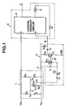
- the construction may be such that the monitoring circuit monitors for the normalcy of the oscillation circuit based on a signal change which is produced only when the oscillation circuit is operating normally, and when the oscillation circuit is a PUT oscillation circuit which uses a PUT for the switching element, there is provided: a differentiating circuit for differentiating a cathode terminal voltage of the PUT; a photocoupler comprising a photodiode with an anode side connected to a constant voltage line and a cathode side connected to an output terminal of the differentiating circuit, and a phototransistor with a collector side connected to the constant voltage line via a resistor, and an emitter side connected to earth; and a level conversion circuit comprising a capacitor and a diode with the capacitor connected between an intermediate point between the resistor and the phototransistor and a cathode side of the diode, and an anode side of the diode connected to the constant voltage line, and an output signal from the level conversion circuit is
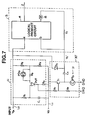
- the construction may be such that the monitoring circuit monitors for the normalcy of the oscillation circuit based on a sequential signal change in the various parts of the oscillation circuit for when the oscillation circuit is operating normally, and when the oscillation circuit is a PUT oscillation circuit which uses a PUT for the switching element, there is provided: a first photocoupler comprising a first photodiode and a first phototransistor, for detecting the presence of a gate current of the PUT of the oscillation circuit; a second photocoupler comprising a second photodiode and a second phototransistor, for detecting the presence of an anode current of the PUT of the oscillation circuit; a voltage dividing circuit for dividing a cathode voltage of the PUT; a transistor with an emitter side connected to a constant voltage line and a collector side connected to a collector side of the second phototransistor, and a voltage divided by the voltage dividing circuit input to a base terminal; and a level conversion circuit comprising
- the construction may be such that the monitoring circuit monitors for the normalcy of the oscillation circuit based on a sequential signal change in the various parts of the oscillation circuit for when the oscillation circuit is operating normally, and when the oscillation circuit is a PUT oscillation circuit which uses a PUT for the switching element, there is provided: a first photocoupler comprising a first photodiode and a first phototransistor, for detecting the presence of a gate current of the PUT of the oscillation circuit; a second photocoupler comprising a second photodiode and a second phototransistor, for detecting the presence of an anode current of the PUT of the oscillation circuit; a voltage dividing circuit for dividing a cathode voltage of the PUT; a transistor with an emitter side connected to a constant voltage line and a collector side connected to a collector side of the second phototransistor, and a voltage divided by the voltage dividing circuit input to a base terminal; and a level conversion circuit comprising
- the monitoring circuit 12 comprises: a capacitor C 2 with one end connected to an intermediate point between a cathode terminal of the PUT of the PUT oscillation circuit 11 and the resistor R 4 ; a resistor R 5 connected to the other end of the capacitor C 2 ; a photocoupler 20 comprising a photodiode PD 1 with an anode side connected to a constant voltage line L 1 to which a power source potential Vcc is applied, and a cathode side connected to the resistor R 5 , and a phototransistor PT 1 with a collector side connected to the constant voltage line L 1 via a resistor R 6 , and an emitter side connected to earth (shown as GND in the figure); a diode D 1 with a cathode side connected to the constant voltage line L 1 in parallel with the photodiode PD 1 of the photocoupler 20 and an anode side connected to an intermediate point between the resistor R 5 and the cathode side of the photodiode PD 1
- capacitor C 2 and the resistor R 5 constitute a differentiating circuit for differentiating the cathode voltage V K of the PUT, while the capacitor C 3 and the diode D 2 constitute a level conversion circuit for level converting the output from the photocoupler 20.
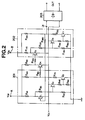
- the circuit of FIG. 2 oscillates and an alternating current output signal is produced at a terminal Uf.
- This alternating current output signal is rectified in the rectifying circuit 203 to become a direct current output signal.
- the normalcy of the PUT oscillation circuit 11 is verified by monitoring the cathode terminal voltage V K of the PUT oscillation circuit 11.
- a monitoring circuit 30 comprises: resistors R 7 , R 8 for voltage dividing the cathode terminal voltage V K of a PUT; a transistor Tr 1 with an emitter terminal connected to a constant voltage line L 1 and a collector terminal connected to a collector terminal of a phototransistor PT 31 of a photocoupler 31 to be described later, and a voltage divided by the beforementioned resistors R 7 , R 8 applied to a base terminal; a photocoupler 31 comprising a photodiode PD 31 disposed between a gate terminal of the PUT and an intermediate point between resistors R 2 and R 3 , and the beforementioned phototransistor PT 31 ; a capacitor C 4 with one end connected to an intermediate point between the transistor Tr 1 and the phototransistor PT 31 ; and a diode D 3 with a cathode terminal connected to the other end of the capacitor C 4 and an anode terminal connected to the constant voltage line L 1 .
- the resistors R 7 , R 8 for voltage
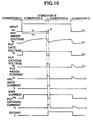
- the PUT oscillation circuit 11 becomes condition A and the PUT goes off.
- the gate current i G is thus zero and hence the phototransistor PT 31 is off, giving a high impedance.
- a base terminal voltage V ⁇ of the transistor Tr 1 falls to a level where the transistor Tr 1 comes on.
- a collector terminal voltage V ⁇ of the transistor Tr 1 is approximately at the power source potential Vcc, and the cathode terminal voltage of the diode D 3 is also approximately at the power source potential Vcc. Consequently the capacitor C 4 is in the nearly discharged condition.
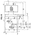
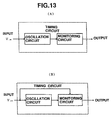
- the cases as shown in FIG. 13 can be considered where, for the signal input condition to the monitoring circuit, then as shown in FIG. 13 (A), only the signal information from the oscillation circuit is received (corresponding to the embodiments of FIG. 1, FIG. 5 and FIG. 8), and, as shown in FIG. 13 (B), in addition to the signal information from the oscillation circuit, the input signal for input to the oscillation circuit is also directly received (corresponding to the embodiments of FIG. 4, FIG. 7, FIG. 10 and FIG. 11).
- the signal input line to the PUT oscillation circuit 11 and the signal input line to the first terminal a can be in separate systems, so that as a result for example of a short circuit fault, the feedback input will not be input to the first terminal a.
- the oscillation circuit and the monitoring circuit malfunction, it is possible to prevent the generation of an erroneous delay output signal.
- the fail-safe characteristics of the on-delay circuit can be increased.
- the fail-safe characteristics of the on-delay circuit can be further improved.
Landscapes
- Electronic Switches (AREA)
- Logic Circuits (AREA)
Applications Claiming Priority (4)
| Application Number | Priority Date | Filing Date | Title |
|---|---|---|---|
| JP316934/95 | 1995-12-05 | ||
| JP31693495 | 1995-12-05 | ||
| JP7316934A JPH09162714A (ja) | 1995-12-05 | 1995-12-05 | フェールセーフな計時回路及びこの計時回路を用いたオン・ディレー回路 |
| PCT/JP1996/003569 WO1997021271A1 (fr) | 1995-12-05 | 1996-12-05 | Circuit temporisateur a securite intrinseque et circuit temporise a la fermeture l'utilisant |
Publications (3)
| Publication Number | Publication Date |
|---|---|
| EP0808026A1 true EP0808026A1 (fr) | 1997-11-19 |
| EP0808026A4 EP0808026A4 (fr) | 1999-06-23 |
| EP0808026B1 EP0808026B1 (fr) | 2002-11-06 |
Family
ID=18082568
Family Applications (1)
| Application Number | Title | Priority Date | Filing Date |
|---|---|---|---|
| EP96941183A Expired - Lifetime EP0808026B1 (fr) | 1995-12-05 | 1996-12-05 | Circuit temporisateur a securite intrinseque et circuit temporise a la fermeture l'utilisant |
Country Status (5)
| Country | Link |
|---|---|
| US (1) | US6239956B1 (fr) |
| EP (1) | EP0808026B1 (fr) |
| JP (1) | JPH09162714A (fr) |
| DE (1) | DE69624684T2 (fr) |
| WO (1) | WO1997021271A1 (fr) |
Families Citing this family (6)
| Publication number | Priority date | Publication date | Assignee | Title |
|---|---|---|---|---|
| JP4355058B2 (ja) | 1999-07-27 | 2009-10-28 | 日本信号株式会社 | 電源装置 |
| JP4531178B2 (ja) | 2000-01-06 | 2010-08-25 | 日本信号株式会社 | 光バリア装置 |
| USD508027S1 (en) * | 2004-12-13 | 2005-08-02 | Yuen Kim Shingt | Power distribution center housing |
| US9344803B1 (en) | 2012-06-21 | 2016-05-17 | Gonzalo Palenzuela | Easy mounting configuration for loudspeaker |
| WO2014063306A1 (fr) * | 2012-10-23 | 2014-05-01 | Abb Technology Ltd | Appareil et procédé de transmission de signal analogique, et multiplexeur de signaux analogiques |
| US9589443B2 (en) | 2014-09-02 | 2017-03-07 | At&T Intellectual Property I, L.P. | Method and apparatus for providing an emergency notification for an allergic reaction |
Family Cites Families (8)
| Publication number | Priority date | Publication date | Assignee | Title |
|---|---|---|---|---|
| JPS60227326A (ja) * | 1984-04-25 | 1985-11-12 | 日本信号株式会社 | 負荷駆動用スイツチ回路の監視装置 |
| JPH0650811B2 (ja) * | 1985-10-31 | 1994-06-29 | 日本信号株式会社 | オン.デイレ−回路 |
| DE3752132T2 (de) * | 1987-06-09 | 1998-05-07 | Koichi Futsuhara | Vorrichtung zur führung eines flugzeugs auf dem boden |
| JPS6423006A (en) * | 1987-07-18 | 1989-01-25 | Ogata Tekko Kk | Burner device |
| JPH02141122A (ja) * | 1988-11-22 | 1990-05-30 | Koji Sato | 遅延回路 |
| DE69315071T2 (de) * | 1993-03-31 | 1998-03-26 | Nippon Signal Co Ltd | Einschaltverzögerungsschaltung |
| JP2683608B2 (ja) * | 1993-12-13 | 1997-12-03 | 日本信号株式会社 | オン.ディレー回路 |
| US5867775A (en) * | 1994-10-28 | 1999-02-02 | The Nippon Signal Co., Ltd. | Fail-safe signal transmitting apparatus producing a logical product of an input signal and a carrier signal |
-
1995
- 1995-12-05 JP JP7316934A patent/JPH09162714A/ja active Pending
-
1996
- 1996-12-05 WO PCT/JP1996/003569 patent/WO1997021271A1/fr not_active Ceased
- 1996-12-05 EP EP96941183A patent/EP0808026B1/fr not_active Expired - Lifetime
- 1996-12-05 US US08/913,143 patent/US6239956B1/en not_active Expired - Fee Related
- 1996-12-05 DE DE69624684T patent/DE69624684T2/de not_active Expired - Fee Related
Also Published As
| Publication number | Publication date |
|---|---|
| US6239956B1 (en) | 2001-05-29 |
| DE69624684T2 (de) | 2003-09-18 |
| JPH09162714A (ja) | 1997-06-20 |
| DE69624684D1 (de) | 2002-12-12 |
| EP0808026A4 (fr) | 1999-06-23 |
| WO1997021271A1 (fr) | 1997-06-12 |
| EP0808026B1 (fr) | 2002-11-06 |
Similar Documents
| Publication | Publication Date | Title |
|---|---|---|
| EP0055816B1 (fr) | Circuit de surveillance de l'action d'un commutateur électrique | |
| US4730121A (en) | Power controller for circuits with battery backup | |
| US4345253A (en) | Passive sensing and encoding transponder | |
| EP0819071B1 (fr) | Circuit de commande de l'alimentation en courant d'un systeme et d'un element d'allumage | |
| EP0644655B1 (fr) | Circuit temporise | |
| JP3773956B2 (ja) | 差動バスを介してデータを伝送するシステム | |
| EP0808026B1 (fr) | Circuit temporisateur a securite intrinseque et circuit temporise a la fermeture l'utilisant | |
| US10171070B2 (en) | Signal transmission circuit and power conversion device | |
| US4363030A (en) | Fail-safe instrument system | |
| EP1250606B1 (fr) | Moniteur coupleur à signal numérique magnetique | |
| US20020005731A1 (en) | Electromigration evaluation circuit | |
| US5198700A (en) | Doubletpulse generator | |
| US4866377A (en) | Proximity detector alternately operated to detect and self-check | |
| US6794919B1 (en) | Devices and methods for automatically producing a clock signal that follows the master clock signal | |
| JPH05315931A (ja) | レベルシフト回路 | |
| US4346371A (en) | Alarm circuit | |
| US5014155A (en) | Circuit for protecting input of semiconductor device | |
| TW522407B (en) | On-chip trim link sensing and latching circuit for fuse links | |
| CA1275458C (fr) | Circuit amplificateur a retablissement rapide | |
| WO1993011610A1 (fr) | Procede et appareil pour surveiller les caracteristiques de fonctionnement de circuits de commutation de courant electrique a semiconducteur | |
| JPH0585082B2 (fr) | ||
| US5818681A (en) | Electromagnetic relay drive circuit | |
| EP0190427B1 (fr) | Système pour détecter des erreurs logiques stochastiques pour réseaux logiques différentiels | |
| JP3287446B2 (ja) | ロック狂い検出装置 | |
| JPH029738B2 (fr) |
Legal Events
| Date | Code | Title | Description |
|---|---|---|---|
| PUAI | Public reference made under article 153(3) epc to a published international application that has entered the european phase |
Free format text: ORIGINAL CODE: 0009012 |
|
| AK | Designated contracting states |
Kind code of ref document: A1 Designated state(s): DE FR GB |
|
| 17P | Request for examination filed |
Effective date: 19971201 |
|
| A4 | Supplementary search report drawn up and despatched |
Effective date: 19990511 |
|
| AK | Designated contracting states |
Kind code of ref document: A4 Designated state(s): DE FR GB |
|
| RIC1 | Information provided on ipc code assigned before grant |
Free format text: 6H 03K 17/292 A, 6H 03K 5/153 B |
|
| 17Q | First examination report despatched |
Effective date: 20010710 |
|
| GRAG | Despatch of communication of intention to grant |
Free format text: ORIGINAL CODE: EPIDOS AGRA |
|
| GRAG | Despatch of communication of intention to grant |
Free format text: ORIGINAL CODE: EPIDOS AGRA |
|
| GRAH | Despatch of communication of intention to grant a patent |
Free format text: ORIGINAL CODE: EPIDOS IGRA |
|
| GRAH | Despatch of communication of intention to grant a patent |
Free format text: ORIGINAL CODE: EPIDOS IGRA |
|
| GRAA | (expected) grant |
Free format text: ORIGINAL CODE: 0009210 |
|
| AK | Designated contracting states |
Kind code of ref document: B1 Designated state(s): DE FR GB |
|
| REG | Reference to a national code |
Ref country code: GB Ref legal event code: FG4D |
|
| PGFP | Annual fee paid to national office [announced via postgrant information from national office to epo] |
Ref country code: GB Payment date: 20021204 Year of fee payment: 7 |
|
| REF | Corresponds to: |
Ref document number: 69624684 Country of ref document: DE Date of ref document: 20021212 |
|
| PGFP | Annual fee paid to national office [announced via postgrant information from national office to epo] |
Ref country code: FR Payment date: 20021213 Year of fee payment: 7 |
|
| PGFP | Annual fee paid to national office [announced via postgrant information from national office to epo] |
Ref country code: DE Payment date: 20030226 Year of fee payment: 7 |
|
| ET | Fr: translation filed | ||
| PLBE | No opposition filed within time limit |
Free format text: ORIGINAL CODE: 0009261 |
|
| STAA | Information on the status of an ep patent application or granted ep patent |
Free format text: STATUS: NO OPPOSITION FILED WITHIN TIME LIMIT |
|
| 26N | No opposition filed |
Effective date: 20030807 |
|
| PG25 | Lapsed in a contracting state [announced via postgrant information from national office to epo] |
Ref country code: GB Free format text: LAPSE BECAUSE OF NON-PAYMENT OF DUE FEES Effective date: 20031205 |
|
| PG25 | Lapsed in a contracting state [announced via postgrant information from national office to epo] |
Ref country code: DE Free format text: LAPSE BECAUSE OF NON-PAYMENT OF DUE FEES Effective date: 20040701 |
|
| GBPC | Gb: european patent ceased through non-payment of renewal fee |
Effective date: 20031205 |
|
| PG25 | Lapsed in a contracting state [announced via postgrant information from national office to epo] |
Ref country code: FR Free format text: LAPSE BECAUSE OF NON-PAYMENT OF DUE FEES Effective date: 20041029 |
|
| REG | Reference to a national code |
Ref country code: FR Ref legal event code: ST |
|
| PG25 | Lapsed in a contracting state [announced via postgrant information from national office to epo] |
Ref country code: FR Free format text: LAPSE BECAUSE OF NON-PAYMENT OF DUE FEES Effective date: 20031231 |