EP0806711B1 - Taktselektionsschaltung - Google Patents
Taktselektionsschaltung Download PDFInfo
- Publication number
- EP0806711B1 EP0806711B1 EP19960107337 EP96107337A EP0806711B1 EP 0806711 B1 EP0806711 B1 EP 0806711B1 EP 19960107337 EP19960107337 EP 19960107337 EP 96107337 A EP96107337 A EP 96107337A EP 0806711 B1 EP0806711 B1 EP 0806711B1
- Authority
- EP
- European Patent Office
- Prior art keywords
- input
- latch
- strobe signals
- combining
- signal
- Prior art date
- Legal status (The legal status is an assumption and is not a legal conclusion. Google has not performed a legal analysis and makes no representation as to the accuracy of the status listed.)
- Expired - Lifetime
Links
- 238000000034 method Methods 0.000 claims description 16
- 230000004044 response Effects 0.000 claims description 5
- 230000007704 transition Effects 0.000 claims 2
- 240000007320 Pinus strobus Species 0.000 description 28
- 230000008569 process Effects 0.000 description 4
- 230000001934 delay Effects 0.000 description 3
- 238000010586 diagram Methods 0.000 description 2
- 238000004519 manufacturing process Methods 0.000 description 2
- 238000005259 measurement Methods 0.000 description 2
- 230000000630 rising effect Effects 0.000 description 2
- 239000003990 capacitor Substances 0.000 description 1
- 230000002596 correlated effect Effects 0.000 description 1
- 230000003111 delayed effect Effects 0.000 description 1
- 230000001360 synchronised effect Effects 0.000 description 1
Images
Classifications
-
- G—PHYSICS
- G04—HOROLOGY
- G04F—TIME-INTERVAL MEASURING
- G04F1/00—Apparatus which can be set and started to measure-off predetermined or adjustably-fixed time intervals without driving mechanisms, e.g. egg timers
- G04F1/005—Apparatus which can be set and started to measure-off predetermined or adjustably-fixed time intervals without driving mechanisms, e.g. egg timers using electronic timing, e.g. counting means
Definitions
- the present invention relates generally to digital devices and more particularly to the implementation of timing circuitry using digital devices.
- IC fabrication processes tend to be targeted at one of two applications. Some allow chips to be made with precision passive components (resistors, capacitors, etc.) while others allow very dense areas of transistors to be placed. The former are required for chips with a mostly analogue function and will use Bipolar (and maybe MOSFET) transistors. The latter are targeted at large digital chips and will use MOSFET transistors exclusively.
- the present invention provides an implementation of timing circuits, which are specified by a minimum and maximum value and intended for analogue implementation, using a digital counter and a clock signal of varying phase thus eliminating the need for passive components.
- US-A-3 502 991 discloses an apparatus implementing a timer comprising selection circuitry for selecting from a plurality of input strobe signals to generate an output clock signal, and a counter coupled to said selection circuitry and operable to count a predetermined amount of time in response to said output clock signal.
- the present invention alleviates the inadequacy of the passive components of the IC chips produced, by careful analogue circuit design and by mimicking analogue functions using digital techniques when a large digital device is to incorporate a small analogue selection during the production of mixed signal IC chips with both analogue and digital functional blocks.
- a timer comprising selection circuitry for electing from a plurality of input strobe signals to generate an output clock signal, and a counter couplet to said selection circuitry and operable to count a predetermined amount of time in response to said output clock signal which is built according to the characterising part of claim 1.
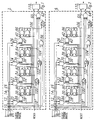
- One embodiment of the present invention as shown in Fig.1 includes a strobe select circuit 7 which uses several input clock signals 10, 12, 14 and 16 having the same frequency, but differing phases to implement a timing circuit.
- These input clock signals 10, 12, 14 and 16 are produced by various techniques including a Delay Locked Loop with multiple variable-delay stages, or by creating increasing delay paths for a single input clock signal.
- the former technique provides for evenly separated phases, while the latter, although much simpler to design, is subject to process, temperature, and voltage level variations.
- Other methods for producing the input clock signals 10, 12, 14 and 16 will be readily apparent to those skilled in the art.
- the number of input clock signals used is determined by the accuracy requirements of the application and by the frequency of a base clock, not shown, from which the input clock signals 10, 12, 14 and 16 are derived.
- the frequency must be a multiple of the shortest timer needed, i.e., if a timer of 50ns (+/-5ns) is needed, then a 10ns or 25ns period is appropriate but a 33ns period is not.
- the range of the exemplary timer is 45-55ns, i.e. 10ns.
- 2 phases give a resolution of 12.5ns
- 4 phases which give a resolution of 6.25ns, are chosen to allow for subsequent gate delays.
- An asserted reset signal 18 holds the circuit 7 or 9 in a reset state, with the output signal at 62 in Fig. 1 and at 64 in Fig. 2 held low.
- Four RS latches 90, 92, 94 and 96 are held reset (where their outputs are HIGH) using this reset signal 18.
- the reset circuits 7 and 9 may be arranged for the signal 18 to be active HIGH or active LOW.
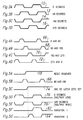
- clock strobes (input signals 10, 12, 14 and 16) are used in the circuits 7 and 9 shown in Figures 1 and 2, respectively, and are called stb0, stb90, stb180 and stb270, respectively, (the numbers referring to their relative phase to the base clock, not shown, from which they are derived).
- the waveforms associated with each of these strobes are shown in Figs. 3A-D, respectively.
- Each pair of adjacent strobes i.e. a pair of strobes separated by 90 degrees
- Each of these signals 66, 68, 70 and 72 are associated with one of the RS latches 90, 92, 94 and 96.
- the number of adjacent strobes AND-ed together so that only one of the combinations is HIGH at any one time depends on the number of input clock strobes used. As an example, if eight clock strobes are used instead of four, four adjacent clock strobes are AND-ed together to give eight signals, only one of which is HIGH at any one time.
- the set input 30 for the RS latch 90 is the NAND 28 of the signal 66 and the output signals 102, 104 and 106 of the other three RS latches 92, 94 and 96.
- NAND gates 32, 36 and 40 are similarly used to generate the set inputs 34, 38 and 42 for the RS latches 92, 94 and 96, respectively.
- the RS latches 90, 92, 94 and 96 are able to be set.
- the NAND gates 28, 32, 36 and 40 on the set inputs 30, 34, 38 and 42 of the RS latches 90, 92, 94 and 96 only one gets set, as shown by the exemplary waveform in Fig.5C, namely the one associated with the two strobe inputs 10 and 12, 12 and 14, 14 and 16, or 16 and 10 which are both HIGH.
- the strobe inputs which are 90 and 180 out of phase from the base clock are selected.
- this RS latch 90, 92, 94 or 96 sets, its output signal 100, 102, 104 or 106 goes LOW which feeds into the NAND gates 28, 32, 36 and 40, respectively, on the other three RS latches and prevents them from being able to be set. So only one RS latch 90, 92, 94 or 96 will ever have its output signal 100, 102, 104 or 106 LOW.
- the output signals 100, 102, 104 and 106 of the four RS latches 90, 92, 94 and 96, respectively, are inverted and fed into NAND gates 52, 54, 56 and 58 respectively, along with one of the input strobes 10, 12, 14 or 16.
- the RS latch 90, 92, 94 or 96 which is set enables its associated strobe signal 10, 12, 14 or 16 to traverse the NAND gate 52, 54, 56 or 58.
- NAND gate 62 (which, by DeMorgan's Theorem implements an OR function) to give the output clock signal 62 in the first embodiment shown in Fig.1 and to give the output clock signal 64 in the second embodiment shown in Fig.2.
- Figs. 1 and 2 Two embodiments of the strobe selection circuit 7 and 9 are shown in Figs. 1 and 2, respectively, the difference being in which strobe signal 10, 12, 14 or 16 gets selected by which RS latch 90, 92, 94 or 96.
- the strobe signal 10, 12, 14 or 16 selected to the output 62 or 64 must either be (upto) halfway through its LOW period, as illustrated by the waveform in Fig.5D, or (upto) halfway HIGH as illustrated by the waveform shown in Fig.5E (the other two could be transitioning LOW to HIGH or HIGH to LOW at this time which gives a very short glitch on the output clock signal 62 or 64), the waveforms of which are shown in Figs.5F and 5G, respectively.
- the final component of a timer in accordance with the present invention is a synchronous count-down counter 110.
- the counter 110 is held reset by the same reset signal 18 as the strobe select circuits 7 and 9 shown in Figs.1 and 2, respectively.
- the counter 110 counts down with each clock edge output 62 or 64 from the strobe select circuits 7 or 9 shown in Figs.1 and 2, respectively.
- the delay to the first rising edge is either upto half a cycle minus delay through two NAND gates, and fanout into the counter in the circuit shown in Fig.1, or just these gate delays in the circuit shown in Fig.2.
Landscapes
- Physics & Mathematics (AREA)
- General Physics & Mathematics (AREA)
- Manipulation Of Pulses (AREA)
- Pulse Circuits (AREA)
Claims (11)
- Vorrichtung für die Implementierung eines Taktgebers, die umfaßt:dadurch gekennzeichnet, daß die Auswahlschaltungsanordnung mehrere Zwischenspeicherschaltungen enthält, die jeweils einen Setzeingang (30, 34, 38, 42) und einen Rücksetzeingang besitzen, vobei jeder Setzeingang auf eine von mehreren Kombinationen aus Eingangs-Strobe-Signalen anspricht und jeder Rücksetzeingang auf ein Rücksetzsignal (18) anspricht.eine Auswahlschaltungsanordnung (7, 9), die eine Auswahl aus mehreren Eingangs-Strobe-Signalen (10, 12, 14, 16) trifft, um ein Ausgangstaktsignal (62, 64) zu erzeugen;einen Zähler (110), der mit der Auswahlschaltungsanordnung verbunden und so betreibbar ist, daß er als Antwort auf das Ausgangstaktsignal eine vorgegebene Zeitperiode zählt; und
- Vorrichtung nach Anspruch 1, bei der jedem der Eingangs-Strobe-Signale eine Frequenz und eine Phase zugeordnet ist, die zugeordnete Frequenz jedes der Eingangs-Strobe-Signale gleich einer Grundfrequenz ist und die zugeordnete Phase jedes der Eingangs-Strobe-Signale eine Verschiebung gegenüber einer Grundphase ist.
- Vorrichtung nach Anspruch 1 oder Anspruch 2, bei der nur eine der mehreren Kombinationen aus Eingangs-Strobe-Signalen zu irgendeinem Zeitpunkt positiv ist.
- Vorrichtung nach einem vorhergehenden Anspruch, bei der das Rücksetzsignal positiv ist und jede der Zwischenspeicherschaltungen so betreibbar ist, daß sie ein Zwischenspeicherausgangssignal erzeugt und als Antwort auf die Tatsache, daß die eine der Kombinationen der Eingangs-Strobe-Signale positiv ist und das Rücksetzsignal nicht positiv ist, verhindert, daß die andere der Zwischenspeicherschaltungen gesetzt wird.
- Vorrichtung nach einem vorhergehenden Anspruch, bei der die Auswahlschaltungsanordnung ferner eine Schaltungsanordnung (52, 54, 56, 58) enthält, die das Zwischenspeicherausgangssignal mit einem der Eingangs-Strobe-Signale kombiniert, um das Ausgangstaktsignal zu erzeugen.
- Vorrichtung nach Anspruch 5, bei der die Kombinationsschaltungsanordnung ferner so betreibbar ist, daß sie das Zwischenspeicherausgangssignal mit einem der Eingangs-Strobe-Signale, das sich nicht in der Nähe einer seiner Übergangszeiten befindet, kombiniert.
- Verfahren für die Implementierung eines Zeitgebers in einer Vorrichtung nach Anspruch 1, bei demmehrere Eingangs-Strobe-Signale erzeugt werden, wovon jedem eine Frequenz, die gleich einer Grundtaktfrequenz ist, und eine Phase, die gleich einer Grundtaktphase zuzüglich einer zugeordneten Verschiebung ist, zugeordnet sind;ausgewählte der mehreren Eingangs-Strobe-Signale (10; 12; 14; 16) kombiniert werden, um mehrere Zwischenspeichereingangssignale zu erzeugen;jedes der Zwischenspeichereingangssignale einem Setzeingang einer der Zwischenspeicherschaltungen zugeordnet wird;ein Rücksetzsignal (118) am Rücksetzeingang der Zwischenspeicherschaltungen nicht positiv angenommen wird, um ein Setzen der Zwischenspeicherschaltungen zu ermöglichen;ein Zwischenspeicherausgangssignal, das einer der Zwischenspeicherschaltungen zugeordnet ist, mit einem der Eingangs-Strobe-Signale kombiniert wird, um ein Ausgangstaktsignal (62; 64) zu erzeugen, das durch jede von mehreren Zwischenspeicherschaltungen (90; 92; 94; 96), die einen zugeordneten Setzeingang (30; 34; 38; 42) und einen Rücksetzeingang besitzen, erzeugt wird; unddas Ausgangstaktsignal einem Eingang eines Zählers (110) zugeordnet wird, wobei der Zähler durch das Rücksetzsignal zurückgesetzt gehalten wird und so betreibbar ist, daß er als Antwort auf den Schritt der Annahme der Nichtpositivität mit dem Ausgangstaktsignal zählt.
- Verfahren nach Anspruch 7, bei dem bei dem Schritt, bei dem ausgewählte der Eingangs-Strobe-Signale ausgewählt werden, ausgewählte der Eingangs-Strobe-Signale in der Weise kombiniert werden, daß nur eines der Zwischenspeichereingangssignale zu einem beliebigen Zeitpunkt einen H-Zustand aufweist.
- Verfahren nach Anspruch 8, bei dem bei dem Schritt, bei dem die Zwischenspeicherausgangssignale kombiniert werden, das Zwischenspeicherausgangssignal, das der einen der Zwischenspeicherschaltungen zugeordnet ist, mit dem einen der Eingangs-Strobe-Signale, das sich nicht in der Nähe einer seiner Übergangszeiten befindet, kombiniert wird.
- Verfahren nach Anspruch 9, bei dem bei dem Schritt, bei dem das Zwischenspeicherausgangssignal kombiniert wird, das Zwischenspeicherausgangssignal, das der einen der Zwischenspeicherschaltungen zugeordnet ist, mit dem einen der Eingangs-Strobe-Signale (78), das sich in der Mitte seines H-Zustands befindet, kombiniert wird
- Verfahren nach Anspruch 9, bei dem bei dem Schritt, bei dem das Zwischenspeicherausgangssignal kombiniert wird, das Zwischenspeicherausgangssignal, das der einen der Zwischenspeicherschaltungen zugeordnet ist, mit dem einen der Eingangs-Strobe-Signale (76), das sich in der Mitte seines L-Zustands befindet, kombiniert wird
Priority Applications (2)
| Application Number | Priority Date | Filing Date | Title |
|---|---|---|---|
| DE1996622843 DE69622843T2 (de) | 1996-05-09 | 1996-05-09 | Taktselektionsschaltung |
| EP19960107337 EP0806711B1 (de) | 1996-05-09 | 1996-05-09 | Taktselektionsschaltung |
Applications Claiming Priority (1)
| Application Number | Priority Date | Filing Date | Title |
|---|---|---|---|
| EP19960107337 EP0806711B1 (de) | 1996-05-09 | 1996-05-09 | Taktselektionsschaltung |
Publications (2)
| Publication Number | Publication Date |
|---|---|
| EP0806711A1 EP0806711A1 (de) | 1997-11-12 |
| EP0806711B1 true EP0806711B1 (de) | 2002-08-07 |
Family
ID=8222766
Family Applications (1)
| Application Number | Title | Priority Date | Filing Date |
|---|---|---|---|
| EP19960107337 Expired - Lifetime EP0806711B1 (de) | 1996-05-09 | 1996-05-09 | Taktselektionsschaltung |
Country Status (2)
| Country | Link |
|---|---|
| EP (1) | EP0806711B1 (de) |
| DE (1) | DE69622843T2 (de) |
Family Cites Families (3)
| Publication number | Priority date | Publication date | Assignee | Title |
|---|---|---|---|---|
| US2928045A (en) * | 1957-09-20 | 1960-03-08 | Itt | Signal decoder |
| US3502991A (en) * | 1967-06-19 | 1970-03-24 | Bell Telephone Labor Inc | Signal generator with asynchronous start |
| JPS58184886A (ja) * | 1982-04-22 | 1983-10-28 | Nippon Hoso Kyokai <Nhk> | クロツク再生方式 |
-
1996
- 1996-05-09 EP EP19960107337 patent/EP0806711B1/de not_active Expired - Lifetime
- 1996-05-09 DE DE1996622843 patent/DE69622843T2/de not_active Expired - Lifetime
Also Published As
| Publication number | Publication date |
|---|---|
| EP0806711A1 (de) | 1997-11-12 |
| DE69622843D1 (de) | 2002-09-12 |
| DE69622843T2 (de) | 2002-11-28 |
Similar Documents
| Publication | Publication Date | Title |
|---|---|---|
| US6285226B1 (en) | Duty cycle correction circuit and method | |
| US5036230A (en) | CMOS clock-phase synthesizer | |
| US5793709A (en) | Free loop interval timer and modulator | |
| EP0600815A2 (de) | Programmierbarer Pulsgenerator mit hoher Auflösung | |
| US4608706A (en) | High-speed programmable timing generator | |
| US4260912A (en) | Digital delay generator | |
| JPH0292012A (ja) | パルス発生回路 | |
| US5666079A (en) | Binary relative delay line | |
| US4638256A (en) | Edge triggered clock distribution system | |
| KR19980078161A (ko) | 반도체 메모리 소자의 딜레이 루프 럭크 회로 | |
| US5903522A (en) | Free loop interval timer and modulator | |
| EP0806711B1 (de) | Taktselektionsschaltung | |
| USRE31551E (en) | Digital delay generator | |
| US6204711B1 (en) | Reduced error asynchronous clock | |
| JPS62111522A (ja) | デイジタル回路 | |
| JPH11163689A (ja) | クロック逓倍回路 | |
| RU2855120C1 (ru) | Способ фазовой синхронизации тактовых импульсов | |
| JP2586712B2 (ja) | 非同期信号選択回路 | |
| JPH0770996B2 (ja) | ギヤツプが付随する書込みクロツクからギヤツプのない読出しクロツクへの変換方法および装置 | |
| JP2543514B2 (ja) | タイミング信号発生器 | |
| JPS6359017A (ja) | パルス発生回路 | |
| JPH03117208A (ja) | データ保持回路 | |
| JPS61243527A (ja) | ビツトバツフア回路 | |
| US20020050846A1 (en) | Method and device for eliminating time delay of an inverted signal | |
| SU760423A1 (ru) | Устройство для задержки импульсов |
Legal Events
| Date | Code | Title | Description |
|---|---|---|---|
| PUAI | Public reference made under article 153(3) epc to a published international application that has entered the european phase |
Free format text: ORIGINAL CODE: 0009012 |
|
| AK | Designated contracting states |
Kind code of ref document: A1 Designated state(s): DE FR GB IT NL |
|
| 17P | Request for examination filed |
Effective date: 19980512 |
|
| 17Q | First examination report despatched |
Effective date: 19990601 |
|
| GRAG | Despatch of communication of intention to grant |
Free format text: ORIGINAL CODE: EPIDOS AGRA |
|
| GRAG | Despatch of communication of intention to grant |
Free format text: ORIGINAL CODE: EPIDOS AGRA |
|
| GRAH | Despatch of communication of intention to grant a patent |
Free format text: ORIGINAL CODE: EPIDOS IGRA |
|
| GRAH | Despatch of communication of intention to grant a patent |
Free format text: ORIGINAL CODE: EPIDOS IGRA |
|
| GRAA | (expected) grant |
Free format text: ORIGINAL CODE: 0009210 |
|
| AK | Designated contracting states |
Kind code of ref document: B1 Designated state(s): DE FR GB IT NL |
|
| PG25 | Lapsed in a contracting state [announced via postgrant information from national office to epo] |
Ref country code: NL Free format text: LAPSE BECAUSE OF FAILURE TO SUBMIT A TRANSLATION OF THE DESCRIPTION OR TO PAY THE FEE WITHIN THE PRESCRIBED TIME-LIMIT Effective date: 20020807 Ref country code: IT Free format text: LAPSE BECAUSE OF FAILURE TO SUBMIT A TRANSLATION OF THE DESCRIPTION OR TO PAY THE FEE WITHIN THE PRE;WARNING: LAPSES OF ITALIAN PATENTS WITH EFFECTIVE DATE BEFORE 2007 MAY HAVE OCCURRED AT ANY TIME BEFORE 2007. THE CORRECT EFFECTIVE DATE MAY BE DIFFERENT FROM THE ONE RECORDED.SCRIBED TIME-LIMIT Effective date: 20020807 |
|
| REG | Reference to a national code |
Ref country code: GB Ref legal event code: FG4D |
|
| REF | Corresponds to: |
Ref document number: 69622843 Country of ref document: DE Date of ref document: 20020912 |
|
| NLV1 | Nl: lapsed or annulled due to failure to fulfill the requirements of art. 29p and 29m of the patents act | ||
| ET | Fr: translation filed | ||
| PLBE | No opposition filed within time limit |
Free format text: ORIGINAL CODE: 0009261 |
|
| STAA | Information on the status of an ep patent application or granted ep patent |
Free format text: STATUS: NO OPPOSITION FILED WITHIN TIME LIMIT |
|
| 26N | No opposition filed |
Effective date: 20030508 |
|
| PGFP | Annual fee paid to national office [announced via postgrant information from national office to epo] |
Ref country code: FR Payment date: 20090507 Year of fee payment: 14 |
|
| REG | Reference to a national code |
Ref country code: FR Ref legal event code: ST Effective date: 20110131 |
|
| PG25 | Lapsed in a contracting state [announced via postgrant information from national office to epo] |
Ref country code: FR Free format text: LAPSE BECAUSE OF NON-PAYMENT OF DUE FEES Effective date: 20100531 |
|
| PGFP | Annual fee paid to national office [announced via postgrant information from national office to epo] |
Ref country code: DE Payment date: 20110531 Year of fee payment: 16 |
|
| PGFP | Annual fee paid to national office [announced via postgrant information from national office to epo] |
Ref country code: GB Payment date: 20120426 Year of fee payment: 17 |
|
| REG | Reference to a national code |
Ref country code: DE Ref legal event code: R119 Ref document number: 69622843 Country of ref document: DE Effective date: 20121201 |
|
| PG25 | Lapsed in a contracting state [announced via postgrant information from national office to epo] |
Ref country code: DE Free format text: LAPSE BECAUSE OF NON-PAYMENT OF DUE FEES Effective date: 20121201 |
|
| GBPC | Gb: european patent ceased through non-payment of renewal fee |
Effective date: 20130509 |
|
| PG25 | Lapsed in a contracting state [announced via postgrant information from national office to epo] |
Ref country code: GB Free format text: LAPSE BECAUSE OF NON-PAYMENT OF DUE FEES Effective date: 20130509 |