EP0806057B1 - Mos transistor - Google Patents
Mos transistor Download PDFInfo
- Publication number
- EP0806057B1 EP0806057B1 EP96935288A EP96935288A EP0806057B1 EP 0806057 B1 EP0806057 B1 EP 0806057B1 EP 96935288 A EP96935288 A EP 96935288A EP 96935288 A EP96935288 A EP 96935288A EP 0806057 B1 EP0806057 B1 EP 0806057B1
- Authority
- EP
- European Patent Office
- Prior art keywords
- channel
- channel length
- transistor
- current
- width
- Prior art date
- Legal status (The legal status is an assumption and is not a legal conclusion. Google has not performed a legal analysis and makes no representation as to the accuracy of the status listed.)
- Expired - Lifetime
Links
- 238000010276 construction Methods 0.000 description 3
- 238000012986 modification Methods 0.000 description 2
- 230000004048 modification Effects 0.000 description 2
- 238000009792 diffusion process Methods 0.000 description 1
- 238000004519 manufacturing process Methods 0.000 description 1
- 238000000034 method Methods 0.000 description 1
- 229910021420 polycrystalline silicon Inorganic materials 0.000 description 1
- 229920005591 polysilicon Polymers 0.000 description 1
Images

Classifications
-
- H—ELECTRICITY
- H10—SEMICONDUCTOR DEVICES; ELECTRIC SOLID-STATE DEVICES NOT OTHERWISE PROVIDED FOR
- H10D—INORGANIC ELECTRIC SEMICONDUCTOR DEVICES
- H10D62/00—Semiconductor bodies, or regions thereof, of devices having potential barriers
- H10D62/10—Shapes, relative sizes or dispositions of the regions of the semiconductor bodies; Shapes of the semiconductor bodies
- H10D62/17—Semiconductor regions connected to electrodes not carrying current to be rectified, amplified or switched, e.g. channel regions
- H10D62/213—Channel regions of field-effect devices
- H10D62/221—Channel regions of field-effect devices of FETs
- H10D62/235—Channel regions of field-effect devices of FETs of IGFETs
Definitions
- MOS transistors are in the fabrication of current mirror circuits which in its basic form comprise two transistors one of which is diode connected and has the input current applied to it and the other of which has its gate and source electrodes connected to the gate and source electrodes, respectively, of the first transistor and produces an output current at its drain electrode which is related to the input current.
- the relationship between the input and output currents depends on the channel width/length quotients of the transistors. In order to obtain an accurate ratio between the input and output currents it is normal to use a common channel length and vary only the channel width to obtain the desired current ratio because the relationship between the current and channel width is more linear than the relationship between current and channel length.
- Transistor dimensions normally have to fit a resolution grid which means there is a minimum step between the possible channel widths available. Consequently there is a limit to the current ratios available, that is integer ratios may be obtained relatively easily but fractional ratios may be difficult to achieve with accuracy.
- US-A-5 362 988 discloses a mid rail generator circuit which uses a number of current mirror circuits. In this document all the channel lengths are kept the same and the channel widths are varied to produce the desired current ratios. In addition in order to obtain an integer multiplication a number of identical transistors are connected in parallel. While these arrangements are adequate to produce integer or simple fractional current ratios they become unwieldy for producing accurate non simple ratios unless transistor sizes are large.
- CMOS Analogue Circuit Design by Philip E. Allen and Douglas R. Holberg, published by Holt, Rinehart and Winston Inc. (ISBN 0 -03 - 006587-9) at pages 231 and 232 discusses the dimensioning of transistors in current amplifiers but is primarily concerned with integer multiplying factors. It states that it is usual to scale the channel widths rather than the channel length because the length tolerances are greater than the width tolerances due to out diffusion under the polysilicon gate.
- the invention provides an MOS transistor in which the channel length and channel width are multiples of a minimum resolution grid unit, the channel area being substantially rectangular, the channel length forming one side of the rectangle and the channel width a perpendicular side of the rectangle characterised in that the channel length over a first part of the width of the rectangle is different from the channel length over a second part of the width of the rectangle by one or more minimum resolution grid units.
- the invention further provides a current mirror circuit comprising a first diode connected MOS transistor for receiving an input current and a second MOS transistor for producing an output current at its drain electrode, respective gate and source electrodes of the first transistor being connected to those of the second transistor characterised in that the first and/or second transistor is/are an MOS transistor as set forth above.
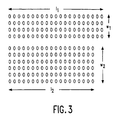
- FIG. 1 a resolution grid is shown where the transistor channel is represented as twenty grid units in length (I) and ten grid units in width (w). If it is desired to construct a current mirror circuit having a given current ratio using a further transistor using the same resolution grid and having the same channel length then the minimum change in width is one resolution unit, i.e. 10% of the width. Consequently the current ratio can only be selected in 10% steps.
- Figure 2 illustrates a refinement which can be used when at least one of the transistors can be divided into two or more narrower transistor segments connected in parallel.
- a unit change in width again gives a 10% current change but if instead one half is given a unit change in length a 2.5% current change is produced.
- This principle is limited by the minimum segment width but will, of course, allow smaller steps if more than two parallel transistors can be implemented.
- a further possibility which enables a small increment in effective channel width and length is to have two or more parallel segments and to alter both the widths and lengths of each segment.
- one of the segments I 1 , w 1 is four units wide and twenty one units long while the other segment I 2 , w 2 is nineteen units long and six units wide. This gives a 1% current step.
- the current step resolution has been increased by a factor of five. If the transistor can be divided into more than two narrower segments a further increase in current step resolution can be achieved using this principle.
- channel length is such that a unit increase or decrease is only a small percentage of the nominal channel length and should preferably be kept below 10% thereof.
- the invention allows current ratios in current mirror circuits using MOS transistors to be selected in 1% steps. Larger sized transistors would, of course, enable even small increments to be achieved while if coarser steps can be tolerated smaller devices may be usable. i.e. having dimensions which are a smaller number of grid resolution units.
Landscapes
- Metal-Oxide And Bipolar Metal-Oxide Semiconductor Integrated Circuits (AREA)
- Amplifiers (AREA)
Description
Claims (3)
- An MOS transistor in which the channel length and channel width are multiples of a minimum resolution grid unit, the channel area being substantially rectangular, the channel length forming one side of the rectangle and the channel width a perpendicular side of the rectangle characterised in that the channel length over a first part of the width of the rectangle is different from the channel length over a second part of the width of the rectangle by one or more minimum resolution grid units.
- An MOS transistor as claimed in Claim 1 comprising two sub-transistors, the channel length of one of the sub-transistors being one resolution grid unit less than the nominal channel length and the channel length of the other sub-transistor being one resolution grid unit greater than the nominal channel length.
- A current mirror circuit comprising a first diode connected MOS transistor for receiving an input current and a second MOS transistor for producing an output current at its drain electrode, respective gate and source electrodes of the first transistor being connected to those of the second transistor characterised in that the first and/or second transistor is/are an MOS transistor as claimed in Claim 1 or Claim 2.
Applications Claiming Priority (3)
| Application Number | Priority Date | Filing Date | Title |
|---|---|---|---|
| GB9524334 | 1995-11-28 | ||
| GBGB9524334.1A GB9524334D0 (en) | 1995-11-28 | 1995-11-28 | Mos transistor |
| PCT/IB1996/001256 WO1997020352A1 (en) | 1995-11-28 | 1996-11-19 | Mos transistor |
Publications (2)
| Publication Number | Publication Date |
|---|---|
| EP0806057A1 EP0806057A1 (en) | 1997-11-12 |
| EP0806057B1 true EP0806057B1 (en) | 2001-09-26 |
Family
ID=10784587
Family Applications (1)
| Application Number | Title | Priority Date | Filing Date |
|---|---|---|---|
| EP96935288A Expired - Lifetime EP0806057B1 (en) | 1995-11-28 | 1996-11-19 | Mos transistor |
Country Status (7)
| Country | Link |
|---|---|
| US (1) | US6445034B1 (en) |
| EP (1) | EP0806057B1 (en) |
| JP (1) | JPH11500582A (en) |
| KR (1) | KR100447381B1 (en) |
| DE (1) | DE69615536T2 (en) |
| GB (1) | GB9524334D0 (en) |
| WO (1) | WO1997020352A1 (en) |
Families Citing this family (3)
| Publication number | Priority date | Publication date | Assignee | Title |
|---|---|---|---|---|
| CA2585659A1 (en) * | 2004-11-05 | 2006-06-22 | Cephalon, Inc. | Cancer treatments |
| DE102004062357A1 (en) * | 2004-12-14 | 2006-07-06 | Atmel Germany Gmbh | Supply circuit for generating a reference current with predeterminable temperature dependence |
| US9466669B2 (en) | 2014-05-05 | 2016-10-11 | Samsung Electronics Co., Ltd. | Multiple channel length finFETs with same physical gate length |
Family Cites Families (9)
| Publication number | Priority date | Publication date | Assignee | Title |
|---|---|---|---|---|
| JPS6022354B2 (en) * | 1977-09-20 | 1985-06-01 | 株式会社リコー | Electrostatic latent image development method |
| US4364041A (en) * | 1978-07-12 | 1982-12-14 | Sharp Kabushiki Kaisha | Contrast controllable electrochromic display driver circuit |
| JPS5646556A (en) * | 1979-09-21 | 1981-04-27 | Nec Corp | Field effect transistor |
| US4594577A (en) * | 1980-09-02 | 1986-06-10 | American Microsystems, Inc. | Current mirror digital to analog converter |
| JPH0666339B2 (en) * | 1985-07-01 | 1994-08-24 | 日本電気株式会社 | Two-dimensional electron gas FET |
| JPH0669358B2 (en) * | 1985-07-11 | 1994-09-07 | 千代田化工建設株式会社 | Fermenter |
| JPH01243591A (en) * | 1988-03-25 | 1989-09-28 | Hitachi Ltd | Semiconductor device |
| JP2507007B2 (en) * | 1988-12-09 | 1996-06-12 | 松下電子工業株式会社 | Semiconductor device |
| US5362988A (en) * | 1992-05-01 | 1994-11-08 | Texas Instruments Incorporated | Local mid-rail generator circuit |
-
1995
- 1995-11-28 GB GBGB9524334.1A patent/GB9524334D0/en active Pending
-
1996
- 1996-11-19 DE DE69615536T patent/DE69615536T2/en not_active Expired - Lifetime
- 1996-11-19 JP JP9520317A patent/JPH11500582A/en not_active Abandoned
- 1996-11-19 EP EP96935288A patent/EP0806057B1/en not_active Expired - Lifetime
- 1996-11-19 KR KR1019970705101A patent/KR100447381B1/en not_active Expired - Fee Related
- 1996-11-19 WO PCT/IB1996/001256 patent/WO1997020352A1/en not_active Ceased
- 1996-11-26 US US08/753,556 patent/US6445034B1/en not_active Expired - Lifetime
Also Published As
| Publication number | Publication date |
|---|---|
| DE69615536T2 (en) | 2002-05-08 |
| EP0806057A1 (en) | 1997-11-12 |
| DE69615536D1 (en) | 2001-10-31 |
| KR19980701705A (en) | 1998-06-25 |
| GB9524334D0 (en) | 1996-01-31 |
| US6445034B1 (en) | 2002-09-03 |
| WO1997020352A1 (en) | 1997-06-05 |
| KR100447381B1 (en) | 2004-10-14 |
| JPH11500582A (en) | 1999-01-12 |
Similar Documents
| Publication | Publication Date | Title |
|---|---|---|
| US4692689A (en) | FET voltage reference circuit with threshold voltage compensation | |
| KR970024170A (en) | RESURF EDMOS transistors and high-voltage analog multiplexer circuits using them | |
| JPH0661816A (en) | Circuit arrangement for current limiting of power MOSFETs | |
| WO1994001890A1 (en) | Integrated cmos semiconductor circuit | |
| US6542098B1 (en) | Low-output capacitance, current mode digital-to-analog converter | |
| JPH0321114A (en) | How to drive semiconductor devices | |
| EP0806057B1 (en) | Mos transistor | |
| US5229708A (en) | Integrable shunt regulator | |
| EP0899871B1 (en) | Performance selection in an integrated circuit | |
| DE3913446A1 (en) | POWER MIRROR | |
| US4068140A (en) | MOS source follower circuit | |
| KR970005288B1 (en) | Variable voltage current conversion circuit | |
| DE3303248A1 (en) | Semiconductor circuit corresponding to a higher-power Z diode | |
| US7279880B2 (en) | Temperature independent low voltage reference circuit | |
| KR100298612B1 (en) | CMOS Low Voltage Current Reference | |
| US5239208A (en) | Constant current circuit employing transistors having specific gate dimensions | |
| JP2001109528A (en) | Voltage generation circuit | |
| US20070103845A1 (en) | Circuits and methods for canceling signal dependent capacitance | |
| EP0647027A1 (en) | Low voltage precision current switch | |
| JPH07236269A (en) | Charge pump output voltage control method and control device | |
| EP0404360B1 (en) | Shielded transistor device | |
| EP0913932A2 (en) | A buffering integrated circuit | |
| DE19928796B4 (en) | Electronic switch for switching a load | |
| GB2113934A (en) | Determining switching threshold in CMOS circuits | |
| JPH0634676A (en) | Power supply voltage detection circuit and semiconductor integrated circuit provided with the circuit |
Legal Events
| Date | Code | Title | Description |
|---|---|---|---|
| PUAI | Public reference made under article 153(3) epc to a published international application that has entered the european phase |
Free format text: ORIGINAL CODE: 0009012 |
|
| AK | Designated contracting states |
Kind code of ref document: A1 Designated state(s): DE FR GB IT NL |
|
| 17P | Request for examination filed |
Effective date: 19971205 |
|
| 17Q | First examination report despatched |
Effective date: 19981217 |
|
| GRAG | Despatch of communication of intention to grant |
Free format text: ORIGINAL CODE: EPIDOS AGRA |
|
| GRAG | Despatch of communication of intention to grant |
Free format text: ORIGINAL CODE: EPIDOS AGRA |
|
| GRAG | Despatch of communication of intention to grant |
Free format text: ORIGINAL CODE: EPIDOS AGRA |
|
| GRAH | Despatch of communication of intention to grant a patent |
Free format text: ORIGINAL CODE: EPIDOS IGRA |
|
| GRAH | Despatch of communication of intention to grant a patent |
Free format text: ORIGINAL CODE: EPIDOS IGRA |
|
| GRAA | (expected) grant |
Free format text: ORIGINAL CODE: 0009210 |
|
| AK | Designated contracting states |
Kind code of ref document: B1 Designated state(s): DE FR GB IT NL |
|
| PG25 | Lapsed in a contracting state [announced via postgrant information from national office to epo] |
Ref country code: NL Free format text: LAPSE BECAUSE OF FAILURE TO SUBMIT A TRANSLATION OF THE DESCRIPTION OR TO PAY THE FEE WITHIN THE PRESCRIBED TIME-LIMIT Effective date: 20010926 Ref country code: IT Free format text: LAPSE BECAUSE OF FAILURE TO SUBMIT A TRANSLATION OF THE DESCRIPTION OR TO PAY THE FEE WITHIN THE PRESCRIBED TIME-LIMIT;WARNING: LAPSES OF ITALIAN PATENTS WITH EFFECTIVE DATE BEFORE 2007 MAY HAVE OCCURRED AT ANY TIME BEFORE 2007. THE CORRECT EFFECTIVE DATE MAY BE DIFFERENT FROM THE ONE RECORDED. Effective date: 20010926 |
|
| REF | Corresponds to: |
Ref document number: 69615536 Country of ref document: DE Date of ref document: 20011031 |
|
| REG | Reference to a national code |
Ref country code: GB Ref legal event code: IF02 |
|
| ET | Fr: translation filed | ||
| NLV1 | Nl: lapsed or annulled due to failure to fulfill the requirements of art. 29p and 29m of the patents act | ||
| PLBE | No opposition filed within time limit |
Free format text: ORIGINAL CODE: 0009261 |
|
| STAA | Information on the status of an ep patent application or granted ep patent |
Free format text: STATUS: NO OPPOSITION FILED WITHIN TIME LIMIT |
|
| 26N | No opposition filed | ||
| REG | Reference to a national code |
Ref country code: GB Ref legal event code: 746 Effective date: 20020917 |
|
| REG | Reference to a national code |
Ref country code: FR Ref legal event code: D6 |
|
| PGFP | Annual fee paid to national office [announced via postgrant information from national office to epo] |
Ref country code: GB Payment date: 20051129 Year of fee payment: 10 Ref country code: FR Payment date: 20051129 Year of fee payment: 10 |
|
| GBPC | Gb: european patent ceased through non-payment of renewal fee |
Effective date: 20061119 |
|
| REG | Reference to a national code |
Ref country code: FR Ref legal event code: ST Effective date: 20070731 |
|
| PG25 | Lapsed in a contracting state [announced via postgrant information from national office to epo] |
Ref country code: GB Free format text: LAPSE BECAUSE OF NON-PAYMENT OF DUE FEES Effective date: 20061119 |
|
| PG25 | Lapsed in a contracting state [announced via postgrant information from national office to epo] |
Ref country code: FR Free format text: LAPSE BECAUSE OF NON-PAYMENT OF DUE FEES Effective date: 20061130 |
|
| REG | Reference to a national code |
Ref country code: DE Ref legal event code: R082 Ref document number: 69615536 Country of ref document: DE Representative=s name: EISENFUEHR SPEISER PATENTANWAELTE RECHTSANWAEL, DE |
|
| REG | Reference to a national code |
Ref country code: DE Ref legal event code: R082 Ref document number: 69615536 Country of ref document: DE Representative=s name: WAGNER & GEYER PARTNERSCHAFT MBB PATENT- UND R, DE Effective date: 20150129 Ref country code: DE Ref legal event code: R082 Ref document number: 69615536 Country of ref document: DE Representative=s name: EISENFUEHR SPEISER PATENTANWAELTE RECHTSANWAEL, DE Effective date: 20150129 Ref country code: DE Ref legal event code: R081 Ref document number: 69615536 Country of ref document: DE Owner name: SNAP TRACK, INC., SAN DIEGO, US Free format text: FORMER OWNER: NXP B.V., EINDHOVEN, NL Effective date: 20150129 Ref country code: DE Ref legal event code: R081 Ref document number: 69615536 Country of ref document: DE Owner name: ST-ERICSSON SA, PLAN-LES-OUATES, CH Free format text: FORMER OWNER: NXP B.V., EINDHOVEN, NL Effective date: 20150129 |
|
| REG | Reference to a national code |
Ref country code: DE Ref legal event code: R082 Ref document number: 69615536 Country of ref document: DE Representative=s name: WAGNER & GEYER PARTNERSCHAFT MBB PATENT- UND R, DE Ref country code: DE Ref legal event code: R082 Ref document number: 69615536 Country of ref document: DE Representative=s name: EISENFUEHR SPEISER PATENTANWAELTE RECHTSANWAEL, DE Ref country code: DE Ref legal event code: R081 Ref document number: 69615536 Country of ref document: DE Owner name: SNAP TRACK, INC., SAN DIEGO, US Free format text: FORMER OWNER: ST-ERICSSON SA, PLAN-LES-OUATES, GENEVA, CH |
|
| REG | Reference to a national code |
Ref country code: DE Ref legal event code: R082 Ref document number: 69615536 Country of ref document: DE Representative=s name: WAGNER & GEYER PARTNERSCHAFT MBB PATENT- UND R, DE |
|
| PGFP | Annual fee paid to national office [announced via postgrant information from national office to epo] |
Ref country code: DE Payment date: 20151130 Year of fee payment: 20 |
|
| REG | Reference to a national code |
Ref country code: DE Ref legal event code: R071 Ref document number: 69615536 Country of ref document: DE |