EP0805579A2 - Démodulateur pour un signal modulé en largeur d'impulsion - Google Patents
Démodulateur pour un signal modulé en largeur d'impulsion Download PDFInfo
- Publication number
- EP0805579A2 EP0805579A2 EP97302618A EP97302618A EP0805579A2 EP 0805579 A2 EP0805579 A2 EP 0805579A2 EP 97302618 A EP97302618 A EP 97302618A EP 97302618 A EP97302618 A EP 97302618A EP 0805579 A2 EP0805579 A2 EP 0805579A2
- Authority
- EP
- European Patent Office
- Prior art keywords
- value
- pwm signal
- counter
- count
- frequency
- Prior art date
- Legal status (The legal status is an assumption and is not a legal conclusion. Google has not performed a legal analysis and makes no representation as to the accuracy of the status listed.)
- Granted
Links
- 238000000034 method Methods 0.000 claims description 16
- 230000000630 rising effect Effects 0.000 claims description 15
- 230000001419 dependent effect Effects 0.000 claims description 3
- 238000010586 diagram Methods 0.000 description 2
- 230000000694 effects Effects 0.000 description 2
- 238000005259 measurement Methods 0.000 description 2
- 238000012986 modification Methods 0.000 description 2
- 230000004048 modification Effects 0.000 description 2
- 230000005540 biological transmission Effects 0.000 description 1
- 238000010276 construction Methods 0.000 description 1
- 238000013461 design Methods 0.000 description 1
- 238000010348 incorporation Methods 0.000 description 1
- 238000013139 quantization Methods 0.000 description 1
- 238000005070 sampling Methods 0.000 description 1
- 239000007787 solid Substances 0.000 description 1
- 230000001960 triggered effect Effects 0.000 description 1
Images


Classifications
-
- H—ELECTRICITY
- H03—ELECTRONIC CIRCUITRY
- H03K—PULSE TECHNIQUE
- H03K7/00—Modulating pulses with a continuously-variable modulating signal
- H03K7/08—Duration or width modulation ; Duty cycle modulation
-
- H—ELECTRICITY
- H04—ELECTRIC COMMUNICATION TECHNIQUE
- H04L—TRANSMISSION OF DIGITAL INFORMATION, e.g. TELEGRAPHIC COMMUNICATION
- H04L25/00—Baseband systems
- H04L25/38—Synchronous or start-stop systems, e.g. for Baudot code
- H04L25/40—Transmitting circuits; Receiving circuits
- H04L25/49—Transmitting circuits; Receiving circuits using code conversion at the transmitter; using predistortion; using insertion of idle bits for obtaining a desired frequency spectrum; using three or more amplitude levels ; Baseband coding techniques specific to data transmission systems
- H04L25/4902—Pulse width modulation; Pulse position modulation
Definitions
- the invention relates to a demodulator for a pulse width modulated signal and, in particular, to such a demodulator for measuring the pulse width of a signal of variable pulse frequency.
- a signal comprises a series of pulses at a constant frequency, the "high” or “on” period of the pulse, and hence the width, providing information, for example the sampled amplitude of an analogue signal.
- the information can be represented by the "duty ratio” that is the ratio of the "on” period of the pulse to the sum of the "on” period and the “off” period.
- the sum of the "on” and “off” periods is the constant period of the signal.
- a demodulator for a pulse width modulated (PWM) signal which alternates between first and second states
- the demodulator comprising: a up/down counter having a PWM signal input and a set input for a signal indicative of an event in the PWM signal period to which the counter is responsive to set a predetermined first value therein; count rate setting means for setting a count rate of the counter to count from the predetermined first value to a predetermined second value over the PWM signal period, the up/down counter being responsive to one of the first and second states of the PWM signal at the said event to count in one direction from the first value and, thereafter, responsive to the other of the first and second states of the PWM signal to count in the other direction, such that an output of the up/down counter is a value representative of the duty ratio of the PWM signal.
- PWM pulse width modulated
- the invention provides a demodulator that counts in opposite directions for the high and low parts of the PWM signal.
- the final value of the up and down counting at the end of the PWM signal period is the equivalent of the duty ratio of the PWM signal.
- the invention can be arranged to demodulate PWM signals in which the period, and therefore the frequency, is variable. This is achieved by linking the rate of the count to the prevailing PWM signal period. By this correlation the count rate will be adjusted to the PWM signal period, such that the rate will be higher when the period is short and lower for a longer period.
- the demodulator includes a frequency multiplier, having a system clock input, an up counter, a latch arranged to latch on each PWM signal rising edge, a programmable divider, and a fixed ratio divider arranged to divide by the counting range value, wherein the up counter is arranged to count up at the system clock rate divided by the fixed ratio divider and output a maximum up count value to the latch and the programmable divider is arranged to receive the up count value from the latch and divide the system clock frequency by the latched up count value.
- the counting range value may be determined by deriving the minimum number of up counts of the up counter in the frequency multiplier within a minimum specified PWM period to achieve a desired error value. The system can thus be configured to operate within a desired error tolerance.
- the demodulator may be arranged to output a "no-PWM" signal when the PWM frequency drops below a specified value.
- the up counter of the frequency multiplier may include a predetermined maximum up count value, and the demodulator may be arranged to output a "no-PWM" signal when the maximum up count value is exceeded.
- a pulse width modulated waveform to be measured is generated from an external source, for example from sampling an analogue waveform.
- the analysing system of the present invention is preferably incorporated in an application specific integrated circuit (ASIC) and the waveform is input to the ASIC.
- ASIC application specific integrated circuit
- the system is also suitable for incorporation in a Field Programmable Gate Array.
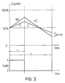
- a sample PWM signal is shown at the bottom of the figure, having a high value "one" and a low value "zero".
- a measurement circuit includes an up/down counter capable of counting over a range between zero and a selected upper number. At the beginning of a cycle of the PWM signal the counter is loaded with a value at the centre point of its range. When the PWM input is high, the counter counts up and when it is low the counter counts down. The counter is set to count at a rate such that if the PWM signal were high for a whole period the counter would reach its upper limit (i.e. up to 100%) exactly at the end of the signal period.
- the input frequency of the PWM is multiplied by 512 and that frequency is used as the clock enable to the counter. This method is satisfactory for those situations where the input frequency of the PWM waveform is known in advance to be either constant or to have very small variations around a constant value.
- Fig. 1 shows the count rate, given by gradient G, of the counter such that if it counted up for the entire PWM period it would reach 100%.
- the counter increments from a start level of 50% along the line G for as long as the PWM signal is high. Once the PWM signal goes low, the counter decrements at an equivalent rate, i.e. along a gradient -G.
- the end count then provides a measure of the PWM duty cycle. For example, for a pulse comprising a short time at value 1 followed by a long time at value 0, the counter will only increment by a small number of counts and then decrement by a larger number of counts toward the zero count. For a pulse comprising 50% at value 1, the counter will increment and decrement by the same number and restore to its 50% level. For a pulse with a long time at value 1, the counter will increment further towards its upper limit and than it decrements toward its lower limit.
- Fig. 2 is a block diagram showing the components of such a PWM signal demodulator.
- the principal components are a PWM input 1, an up/down counter 2 and a frequency multiplier 3.
- the PWM input 1 is fed both to the up/down counter 2 and the frequency multiplier 3.
- the subsystem includes a rising edge detector 4, an M-bit up counter 5, an M-bit latch 6, an M-bit programmable divider 7 and a fixed ratio divider 8.
- the system clock inputs to the frequency multiplier 3 at 9.
- the clock input of the M-bit up counter is coupled to the system clock 9 through the fixed ratio divider 8 with its division ratio defining the multiplication factor of the frequency multiplier.
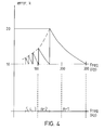
- the up counter 5 is reset each time a rising edge of the PWM signal occurs and then counts up in response to the divided system clock to provide a count output inversely proportional to the PWM frequency. For example if the PWM frequency is low, the counter 5 will be reset relatively infrequently and thus the maximum count will be relatively high. If the PWM input is a high frequency, the up counter 5 will be reset on a more frequent basis and thus the maximum output of the counter 5 would be relatively low.
- the digital output from the up counter 5 is applied to a control input of the M-bit programmable divider 7 via the M-bit latch 6.
- the programmable divider 7 receives at its clock input the system clock 9.
- the programmable divider 7 is of standard construction that will be familiar to those skilled in the art.
- the programmable divider 7 provides an output clock signal that has a frequency that is substantially the PWM input frequency multiplied by the division ratio of the fixed divider 8. This implements equation 1.
- This equation can be derived as follows:
- the PWM signal is connected to the up/down control input of the up/down counter, and a further rising edge detector 10 is also connected to the parallel load control input of the up/down counter 2 to load it at 50% at the beginning of each pulse from an N-bit store (not shown).
- the up/down counter then counts at the rate determined by the frequency of the signal from the frequency multiplier 3 applied to the clock enable input 11.
- An N-bit latch 12 is latched by the rising edge detector to provide an N-bit word representing the duty ratio of the PWM signal.
- FIG. 2 shows two rising edge detectors it will be apparent to the skilled person that a single rising edge detector could be used for both the up/down counter 2 and the frequency multiplier 3.
- This embodiment of the invention provides a system in which the count rate of the up/down counter 21 is locked to the frequency of the incoming PWM waveform such that, in the steady state, it always counts from 50% to 100% of its range in the PWM signal period if the PWM signal is high.
- the circuit automatically compensates for variations in frequency of the incoming PWM waveform.
- the system variables M and N and the system clock frequency define the frequency range and accuracy of the demodulator.
- the accuracy of this circuit depends mainly on the counter 2 being clocked at the correct rate. Since the clock enable input is driven by the output of the frequency multiplier 3, it follows that the accuracy of the circuit depends on the correct counting of the M-bit counter 5.
- This counter gives a number of counts, m, representing the period of the PWM signal, but will generally have an uncertainty of 1 in the value of m. Where the PWM signal has a low frequency, m is high and the accuracy of the clock enable signals for counter 2 is consequently high.
- the divider 8 will also divide by that factor. For this example, the system clock will be chosen to run at 10MHz.
- the error k causes the up/down counter 2 to count at the wrong rate. For example, while the PWM signal is high, the up/down counter 2 increments at a higher rate, and when the PWM signal goes low it also decrements at the higher rate giving rise to an error in the final count. It will be seen that, dependent on the actual error and the duty cycle of the input signal, the up/down counter 2 may saturate at 100% if k is greater than 1 and the duty cycle is greater than 50% or saturate at 0% if k is greater than 1 and the duty cycle is less than 50%.
- N and M can be chosen for the counters 2 and 5 for a given system clock frequency. Appropriate choices will ensure that, at the highest expected frequency of the input signal, the value m of the counter 5 will be high (say greater than 10) and hence the error k will not introduce a significant error in the final count.
- a "no-PWM” signal is arranged to become high so as to select an analogue demand system at a predetermined lower frequency threshold.
- the "no-PWM” signal can be set high if the up counter reaches a maximum value, known as the "terminal count”. This is shown on Fig. 2 where the output TC goes high when the terminal count is reached and provides a signal on line 13. This signals to other parts of the ASIC (not shown) that the input signal is analogue rather than digital in nature.
- the various circuit components shown as digital components can be replaced, either in whole or in part, by analogue components.
- the up/down counter could be replaced by an analogue integrator if that were preferable in a particular implementation.
- the embodiment of the invention is specifically described in relation to the demodulator being triggered on a rising edge of the PWM signal, it is equally the case that the trigger could occur on any other repeating stable event in the PWM period.
- the event could be a moment a predetermined duration after the start of each PWM cycle which could be a rising or falling edge, depending on the arrangement of the PWM signal.
Landscapes
- Physics & Mathematics (AREA)
- Spectroscopy & Molecular Physics (AREA)
- Engineering & Computer Science (AREA)
- Computer Networks & Wireless Communication (AREA)
- Signal Processing (AREA)
- Analogue/Digital Conversion (AREA)
- Amplifiers (AREA)
- Manipulation Of Pulses (AREA)
- Facsimile Image Signal Circuits (AREA)
Applications Claiming Priority (2)
| Application Number | Priority Date | Filing Date | Title |
|---|---|---|---|
| GB9608819 | 1996-04-30 | ||
| GBGB9608819.0A GB9608819D0 (en) | 1996-04-30 | 1996-04-30 | Demodulator for a pulse width modulated signal |
Publications (3)
| Publication Number | Publication Date |
|---|---|
| EP0805579A2 true EP0805579A2 (fr) | 1997-11-05 |
| EP0805579A3 EP0805579A3 (fr) | 1998-09-23 |
| EP0805579B1 EP0805579B1 (fr) | 2004-07-28 |
Family
ID=10792807
Family Applications (1)
| Application Number | Title | Priority Date | Filing Date |
|---|---|---|---|
| EP97302618A Expired - Lifetime EP0805579B1 (fr) | 1996-04-30 | 1997-04-16 | Démodulateur pour un signal modulé en largeur d'impulsion |
Country Status (7)
| Country | Link |
|---|---|
| US (1) | US5905406A (fr) |
| EP (1) | EP0805579B1 (fr) |
| KR (1) | KR100442649B1 (fr) |
| DE (1) | DE69729972T2 (fr) |
| GB (1) | GB9608819D0 (fr) |
| SG (1) | SG55307A1 (fr) |
| TW (1) | TW418565B (fr) |
Cited By (2)
| Publication number | Priority date | Publication date | Assignee | Title |
|---|---|---|---|---|
| US7201244B2 (en) | 2003-10-03 | 2007-04-10 | Letourneau, Inc. | Vehicle for materials handling and other industrial uses |
| EP3479189A4 (fr) * | 2016-06-30 | 2020-03-11 | Intel IP Corporation | Transfert de données par modulation du signal d'horloge |
Families Citing this family (28)
| Publication number | Priority date | Publication date | Assignee | Title |
|---|---|---|---|---|
| US6157671A (en) * | 1997-11-06 | 2000-12-05 | Caterpillar Inc. | Apparatus and method for digitally monitoring a duty cycle of a pulse width modulated signal |
| JPH11163697A (ja) * | 1997-12-01 | 1999-06-18 | Nec Niigata Ltd | Pwm回路 |
| US6519711B1 (en) * | 1999-09-29 | 2003-02-11 | Agere Systems, Inc. | Method and apparatus for controlling a clocked circuit having a register for storing a bit received from an input terminal and an output terminal connected to clock terminal of the clocked circuit |
| US7626451B2 (en) * | 2002-08-26 | 2009-12-01 | Larry Kirn | Data demodulation using an asynchronous clock |
| US7466770B2 (en) * | 2003-08-05 | 2008-12-16 | Jm Electronics Ltd. Llc | Adaptive pulse width discrimination using an asynchronous clock |
| US7512794B2 (en) * | 2004-02-24 | 2009-03-31 | Intersil Americas Inc. | System and method for authentication |
| US7729427B2 (en) * | 2004-02-24 | 2010-06-01 | Intersil Americas Inc. | Pseudo-synchronous one wire bidirectional bus interface |
| US7596699B2 (en) * | 2004-02-24 | 2009-09-29 | Intersil Americas Inc. | Battery authentication system |
| US7551669B2 (en) * | 2005-04-01 | 2009-06-23 | Harman International Industries, Incorporated | System for multiplexing independent signals |
| KR101147250B1 (ko) | 2006-01-27 | 2012-05-18 | 삼성전자주식회사 | 적응적으로 펄스 폭 변조 신호를 복조하는 복조기 및 복조방법 |
| US7587020B2 (en) * | 2007-04-25 | 2009-09-08 | International Business Machines Corporation | High performance, low power, dynamically latched up/down counter |
| KR101517355B1 (ko) * | 2007-07-16 | 2015-05-04 | 코닌클리케 필립스 엔.브이. | 광원 구동 |
| KR101007617B1 (ko) * | 2008-10-28 | 2011-01-12 | 한전케이디엔주식회사 | 광대역 pwm 신호 복조 장치 |
| US8248230B2 (en) | 2009-02-20 | 2012-08-21 | Redwood Systems, Inc. | Smart power device |
| US8207635B2 (en) * | 2009-02-20 | 2012-06-26 | Redwood Systems, Inc. | Digital switch communication |
| US8427300B2 (en) | 2009-02-20 | 2013-04-23 | Redwood Systems, Inc. | Transmission of power and data with frequency modulation |
| US8558598B2 (en) * | 2009-03-16 | 2013-10-15 | Supertex, Inc. | Phase shift generating circuit |
| US8058750B2 (en) * | 2009-05-14 | 2011-11-15 | Redwood Systems, Inc. | Discharge cycle communication |
| CN102103168A (zh) * | 2009-12-22 | 2011-06-22 | 比亚迪股份有限公司 | 一种检测pwm波的方法及pwm波检测装置 |
| US8699371B2 (en) * | 2011-10-14 | 2014-04-15 | Infineon Technologies Ag | Self synchronizing data communication method and device |
| US8564365B2 (en) | 2012-01-20 | 2013-10-22 | Qualcomm Incorporated | Wide input bit-rate, power efficient PWM decoder |
| JP5664606B2 (ja) * | 2012-07-31 | 2015-02-04 | 株式会社デンソー | 復号化回路 |
| KR101366772B1 (ko) * | 2012-09-24 | 2014-02-26 | 삼성전기주식회사 | 모터 구동 장치 및 모터 제어 방법 |
| JP6229426B2 (ja) * | 2013-10-16 | 2017-11-15 | セイコーエプソン株式会社 | 電子機器、および受信制御方法 |
| CN103633963B (zh) * | 2013-11-11 | 2016-01-27 | 电子科技大学 | 基于单线协议的占空比比较电路及方法 |
| US9813076B1 (en) * | 2016-03-31 | 2017-11-07 | Analog Value Ltd. | Analog to digital converter and a method for analog to digital conversion |
| US20220360272A1 (en) | 2021-05-06 | 2022-11-10 | Apple Inc | Analog to digital converter and a method for analog to digital conversion |
| TWI782841B (zh) * | 2021-12-30 | 2022-11-01 | 新唐科技股份有限公司 | 用於透過脈波調變信號進行控制的電路系統的事件偵測控制器與方法 |
Family Cites Families (9)
| Publication number | Priority date | Publication date | Assignee | Title |
|---|---|---|---|---|
| US3740491A (en) * | 1971-04-23 | 1973-06-19 | Stilwell R | Digital magnetic tape recoring system using symmetrical differential pulse width modulation with a triangular reference signal |
| US4019153A (en) * | 1974-10-07 | 1977-04-19 | The Charles Stark Draper Laboratory, Inc. | Digital phase-locked loop filter |
| US4003083A (en) * | 1975-04-15 | 1977-01-11 | The United States Of America As Represented By The Secretary Of The Navy | Digital data recording and decoding |
| GB2016245A (en) * | 1978-02-20 | 1979-09-19 | Smiths Industries Ltd | Decoding arrangements for digital data |
| ATE3233T1 (de) * | 1978-07-07 | 1983-05-15 | The Post Office | Demodulatoranordnung fuer zweiphasendigitalmodulierte signale. |
| DE3173313D1 (en) * | 1980-09-25 | 1986-02-06 | Toshiba Kk | Clock synchronization signal generating circuit |
| JPH03207115A (ja) * | 1990-01-10 | 1991-09-10 | Otari Kk | Pwm信号の復調方式 |
| KR940007977B1 (ko) * | 1991-12-31 | 1994-08-31 | 현대전자산업 주식회사 | Pwm 신호 발생회로 |
| US5553100A (en) * | 1994-04-01 | 1996-09-03 | National Semiconductor Corporation | Fully digital data separator and frequency multiplier |
-
1996
- 1996-04-30 GB GBGB9608819.0A patent/GB9608819D0/en active Pending
-
1997
- 1997-04-16 EP EP97302618A patent/EP0805579B1/fr not_active Expired - Lifetime
- 1997-04-16 DE DE69729972T patent/DE69729972T2/de not_active Expired - Fee Related
- 1997-04-25 TW TW086105390A patent/TW418565B/zh not_active IP Right Cessation
- 1997-04-28 SG SG1997001341A patent/SG55307A1/en unknown
- 1997-04-30 KR KR1019970016413A patent/KR100442649B1/ko not_active Expired - Fee Related
- 1997-04-30 US US08/845,965 patent/US5905406A/en not_active Expired - Lifetime
Cited By (4)
| Publication number | Priority date | Publication date | Assignee | Title |
|---|---|---|---|---|
| US7201244B2 (en) | 2003-10-03 | 2007-04-10 | Letourneau, Inc. | Vehicle for materials handling and other industrial uses |
| US7318580B2 (en) | 2003-10-03 | 2008-01-15 | Letourneau Technologies, Inc. | Vehicle for materials handling and other industrial uses |
| EP3479189A4 (fr) * | 2016-06-30 | 2020-03-11 | Intel IP Corporation | Transfert de données par modulation du signal d'horloge |
| US10942542B2 (en) | 2016-06-30 | 2021-03-09 | Intel IP Corporation | Data transfer by modulating clock signal |
Also Published As
| Publication number | Publication date |
|---|---|
| MX9703195A (es) | 1998-07-31 |
| KR970072673A (ko) | 1997-11-07 |
| EP0805579B1 (fr) | 2004-07-28 |
| DE69729972T2 (de) | 2005-07-21 |
| DE69729972D1 (de) | 2004-09-02 |
| GB9608819D0 (en) | 1996-07-03 |
| TW418565B (en) | 2001-01-11 |
| US5905406A (en) | 1999-05-18 |
| KR100442649B1 (ko) | 2004-11-03 |
| EP0805579A3 (fr) | 1998-09-23 |
| SG55307A1 (en) | 1998-12-21 |
Similar Documents
| Publication | Publication Date | Title |
|---|---|---|
| EP0805579A2 (fr) | Démodulateur pour un signal modulé en largeur d'impulsion | |
| US5451947A (en) | Modulated dither signal | |
| US5054315A (en) | Coding of the value of several quantities measured in a tire | |
| US20020000800A1 (en) | Precise digital frequency detection | |
| US5367200A (en) | Method and apparatus for measuring the duty cycle of a digital signal | |
| EP0003840A2 (fr) | Méthode et dispositif de conversion d'un signal d'entrée analogique en un signal numériquede sortie et convertisseur analogique-numérique | |
| US7649489B2 (en) | Apparatus for analog/digital conversion of a measurement voltage | |
| US6674387B1 (en) | Pulse width modulation analog to digital conversion | |
| US4224568A (en) | Frequency to digital converter | |
| US4458214A (en) | Fast sampling phase locked loop frequency synthesizer | |
| US4282576A (en) | Indicator diagram based AC electric energy meter | |
| US4544911A (en) | Low cost monotonic digital-to-analog converter | |
| EP0253545A2 (fr) | Mesure de signal | |
| EP0607711A1 (fr) | Compteur électrique à convertisseur sigma-delta à gain variable | |
| EP0535124B1 (fr) | Convertisseur analogique-numerique | |
| EP0381217B1 (fr) | Circuits de commutation pour détecter le niveau des signaux | |
| EP0214869B1 (fr) | Appareil et méthode pour convertir une tension en comptage numérique | |
| JPH0338774B2 (fr) | ||
| US3961282A (en) | Tracking status detector for a digital delay lock loop | |
| MXPA97003195A (en) | Desmodulator for modulated signal of impu width | |
| US5717349A (en) | Wideband digital peak detector | |
| RU2011292C1 (ru) | Устройство автоматической подстройки частоты | |
| SU1265640A1 (ru) | Устройство дл измерени фазы | |
| US5801560A (en) | System for determining time between events using a voltage ramp generator | |
| EP0099203A2 (fr) | Circuits d'extraction de racine carrée |
Legal Events
| Date | Code | Title | Description |
|---|---|---|---|
| PUAI | Public reference made under article 153(3) epc to a published international application that has entered the european phase |
Free format text: ORIGINAL CODE: 0009012 |
|
| AK | Designated contracting states |
Kind code of ref document: A2 Designated state(s): DE ES FR GB IT NL SE |
|
| PUAL | Search report despatched |
Free format text: ORIGINAL CODE: 0009013 |
|
| AK | Designated contracting states |
Kind code of ref document: A3 Designated state(s): DE ES FR GB IT NL SE |
|
| 17P | Request for examination filed |
Effective date: 19981023 |
|
| 17Q | First examination report despatched |
Effective date: 20011129 |
|
| GRAH | Despatch of communication of intention to grant a patent |
Free format text: ORIGINAL CODE: EPIDOS IGRA |
|
| GRAH | Despatch of communication of intention to grant a patent |
Free format text: ORIGINAL CODE: EPIDOS IGRA |
|
| GRAA | (expected) grant |
Free format text: ORIGINAL CODE: 0009210 |
|
| AK | Designated contracting states |
Kind code of ref document: B1 Designated state(s): DE ES FR GB IT NL SE |
|
| PG25 | Lapsed in a contracting state [announced via postgrant information from national office to epo] |
Ref country code: NL Free format text: LAPSE BECAUSE OF FAILURE TO SUBMIT A TRANSLATION OF THE DESCRIPTION OR TO PAY THE FEE WITHIN THE PRESCRIBED TIME-LIMIT Effective date: 20040728 |
|
| REG | Reference to a national code |
Ref country code: GB Ref legal event code: FG4D |
|
| REF | Corresponds to: |
Ref document number: 69729972 Country of ref document: DE Date of ref document: 20040902 Kind code of ref document: P |
|
| PG25 | Lapsed in a contracting state [announced via postgrant information from national office to epo] |
Ref country code: SE Free format text: LAPSE BECAUSE OF FAILURE TO SUBMIT A TRANSLATION OF THE DESCRIPTION OR TO PAY THE FEE WITHIN THE PRESCRIBED TIME-LIMIT Effective date: 20041028 |
|
| PG25 | Lapsed in a contracting state [announced via postgrant information from national office to epo] |
Ref country code: ES Free format text: LAPSE BECAUSE OF FAILURE TO SUBMIT A TRANSLATION OF THE DESCRIPTION OR TO PAY THE FEE WITHIN THE PRESCRIBED TIME-LIMIT Effective date: 20041108 |
|
| NLV1 | Nl: lapsed or annulled due to failure to fulfill the requirements of art. 29p and 29m of the patents act | ||
| ET | Fr: translation filed | ||
| PLBE | No opposition filed within time limit |
Free format text: ORIGINAL CODE: 0009261 |
|
| STAA | Information on the status of an ep patent application or granted ep patent |
Free format text: STATUS: NO OPPOSITION FILED WITHIN TIME LIMIT |
|
| 26N | No opposition filed |
Effective date: 20050429 |
|
| PGFP | Annual fee paid to national office [announced via postgrant information from national office to epo] |
Ref country code: FR Payment date: 20080312 Year of fee payment: 12 Ref country code: DE Payment date: 20080424 Year of fee payment: 12 |
|
| PGFP | Annual fee paid to national office [announced via postgrant information from national office to epo] |
Ref country code: IT Payment date: 20080428 Year of fee payment: 12 |
|
| REG | Reference to a national code |
Ref country code: FR Ref legal event code: ST Effective date: 20091231 |
|
| PG25 | Lapsed in a contracting state [announced via postgrant information from national office to epo] |
Ref country code: DE Free format text: LAPSE BECAUSE OF NON-PAYMENT OF DUE FEES Effective date: 20091103 |
|
| PG25 | Lapsed in a contracting state [announced via postgrant information from national office to epo] |
Ref country code: FR Free format text: LAPSE BECAUSE OF NON-PAYMENT OF DUE FEES Effective date: 20091222 |
|
| PG25 | Lapsed in a contracting state [announced via postgrant information from national office to epo] |
Ref country code: IT Free format text: LAPSE BECAUSE OF NON-PAYMENT OF DUE FEES Effective date: 20090416 |
|
| PGFP | Annual fee paid to national office [announced via postgrant information from national office to epo] |
Ref country code: GB Payment date: 20160405 Year of fee payment: 20 |
|
| REG | Reference to a national code |
Ref country code: GB Ref legal event code: PE20 Expiry date: 20170415 |
|
| PG25 | Lapsed in a contracting state [announced via postgrant information from national office to epo] |
Ref country code: GB Free format text: LAPSE BECAUSE OF EXPIRATION OF PROTECTION Effective date: 20170415 |